JP4823729B2 - 光通信モジュール - Google Patents
光通信モジュール Download PDFInfo
- Publication number
- JP4823729B2 JP4823729B2 JP2006076597A JP2006076597A JP4823729B2 JP 4823729 B2 JP4823729 B2 JP 4823729B2 JP 2006076597 A JP2006076597 A JP 2006076597A JP 2006076597 A JP2006076597 A JP 2006076597A JP 4823729 B2 JP4823729 B2 JP 4823729B2
- Authority
- JP
- Japan
- Prior art keywords
- light emitting
- resin
- emitting element
- peripheral edge
- outer peripheral
- Prior art date
- Legal status (The legal status is an assumption and is not a legal conclusion. Google has not performed a legal analysis and makes no representation as to the accuracy of the status listed.)
- Expired - Fee Related
Links
Images


Classifications
-
- H—ELECTRICITY
- H10—SEMICONDUCTOR DEVICES; ELECTRIC SOLID-STATE DEVICES NOT OTHERWISE PROVIDED FOR
- H10F—INORGANIC SEMICONDUCTOR DEVICES SENSITIVE TO INFRARED RADIATION, LIGHT, ELECTROMAGNETIC RADIATION OF SHORTER WAVELENGTH OR CORPUSCULAR RADIATION
- H10F77/00—Constructional details of devices covered by this subclass
- H10F77/50—Encapsulations or containers
-
- H—ELECTRICITY
- H10—SEMICONDUCTOR DEVICES; ELECTRIC SOLID-STATE DEVICES NOT OTHERWISE PROVIDED FOR
- H10F—INORGANIC SEMICONDUCTOR DEVICES SENSITIVE TO INFRARED RADIATION, LIGHT, ELECTROMAGNETIC RADIATION OF SHORTER WAVELENGTH OR CORPUSCULAR RADIATION
- H10F77/00—Constructional details of devices covered by this subclass
- H10F77/40—Optical elements or arrangements
- H10F77/407—Optical elements or arrangements indirectly associated with the devices
-
- H—ELECTRICITY
- H10—SEMICONDUCTOR DEVICES; ELECTRIC SOLID-STATE DEVICES NOT OTHERWISE PROVIDED FOR
- H10W—GENERIC PACKAGES, INTERCONNECTIONS, CONNECTORS OR OTHER CONSTRUCTIONAL DETAILS OF DEVICES COVERED BY CLASS H10
- H10W90/00—Package configurations
-
- H—ELECTRICITY
- H10—SEMICONDUCTOR DEVICES; ELECTRIC SOLID-STATE DEVICES NOT OTHERWISE PROVIDED FOR
- H10H—INORGANIC LIGHT-EMITTING SEMICONDUCTOR DEVICES HAVING POTENTIAL BARRIERS
- H10H20/00—Individual inorganic light-emitting semiconductor devices having potential barriers, e.g. light-emitting diodes [LED]
- H10H20/80—Constructional details
- H10H20/85—Packages
- H10H20/852—Encapsulations
- H10H20/853—Encapsulations characterised by their shape
-
- H—ELECTRICITY
- H10—SEMICONDUCTOR DEVICES; ELECTRIC SOLID-STATE DEVICES NOT OTHERWISE PROVIDED FOR
- H10W—GENERIC PACKAGES, INTERCONNECTIONS, CONNECTORS OR OTHER CONSTRUCTIONAL DETAILS OF DEVICES COVERED BY CLASS H10
- H10W72/00—Interconnections or connectors in packages
- H10W72/01—Manufacture or treatment
- H10W72/015—Manufacture or treatment of bond wires
- H10W72/01515—Forming coatings
-
- H—ELECTRICITY
- H10—SEMICONDUCTOR DEVICES; ELECTRIC SOLID-STATE DEVICES NOT OTHERWISE PROVIDED FOR
- H10W—GENERIC PACKAGES, INTERCONNECTIONS, CONNECTORS OR OTHER CONSTRUCTIONAL DETAILS OF DEVICES COVERED BY CLASS H10
- H10W72/00—Interconnections or connectors in packages
- H10W72/071—Connecting or disconnecting
- H10W72/075—Connecting or disconnecting of bond wires
-
- H—ELECTRICITY
- H10—SEMICONDUCTOR DEVICES; ELECTRIC SOLID-STATE DEVICES NOT OTHERWISE PROVIDED FOR
- H10W—GENERIC PACKAGES, INTERCONNECTIONS, CONNECTORS OR OTHER CONSTRUCTIONAL DETAILS OF DEVICES COVERED BY CLASS H10
- H10W72/00—Interconnections or connectors in packages
- H10W72/50—Bond wires
- H10W72/531—Shapes of wire connectors
- H10W72/536—Shapes of wire connectors the connected ends being ball-shaped
-
- H—ELECTRICITY
- H10—SEMICONDUCTOR DEVICES; ELECTRIC SOLID-STATE DEVICES NOT OTHERWISE PROVIDED FOR
- H10W—GENERIC PACKAGES, INTERCONNECTIONS, CONNECTORS OR OTHER CONSTRUCTIONAL DETAILS OF DEVICES COVERED BY CLASS H10
- H10W72/00—Interconnections or connectors in packages
- H10W72/50—Bond wires
- H10W72/531—Shapes of wire connectors
- H10W72/5363—Shapes of wire connectors the connected ends being wedge-shaped
-
- H—ELECTRICITY
- H10—SEMICONDUCTOR DEVICES; ELECTRIC SOLID-STATE DEVICES NOT OTHERWISE PROVIDED FOR
- H10W—GENERIC PACKAGES, INTERCONNECTIONS, CONNECTORS OR OTHER CONSTRUCTIONAL DETAILS OF DEVICES COVERED BY CLASS H10
- H10W72/00—Interconnections or connectors in packages
- H10W72/50—Bond wires
- H10W72/541—Dispositions of bond wires
- H10W72/547—Dispositions of multiple bond wires
- H10W72/5473—Dispositions of multiple bond wires multiple bond wires connected to a common bond pad
-
- H—ELECTRICITY
- H10—SEMICONDUCTOR DEVICES; ELECTRIC SOLID-STATE DEVICES NOT OTHERWISE PROVIDED FOR
- H10W—GENERIC PACKAGES, INTERCONNECTIONS, CONNECTORS OR OTHER CONSTRUCTIONAL DETAILS OF DEVICES COVERED BY CLASS H10
- H10W74/00—Encapsulations, e.g. protective coatings
-
- H—ELECTRICITY
- H10—SEMICONDUCTOR DEVICES; ELECTRIC SOLID-STATE DEVICES NOT OTHERWISE PROVIDED FOR
- H10W—GENERIC PACKAGES, INTERCONNECTIONS, CONNECTORS OR OTHER CONSTRUCTIONAL DETAILS OF DEVICES COVERED BY CLASS H10
- H10W90/00—Package configurations
- H10W90/701—Package configurations characterised by the relative positions of pads or connectors relative to package parts
- H10W90/751—Package configurations characterised by the relative positions of pads or connectors relative to package parts of bond wires
- H10W90/754—Package configurations characterised by the relative positions of pads or connectors relative to package parts of bond wires between a chip and a stacked insulating package substrate, interposer or RDL
Landscapes
- Led Device Packages (AREA)
- Light Receiving Elements (AREA)
Description
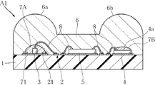
1 基板
2 配線パターン
3 発光素子
4 受光素子
4a 受光面
5 駆動IC(集積回路素子)
6 樹脂パッケージ
6a,6b レンズ
7A,7B 保護樹脂
7Aa (保護樹脂の)外周端縁
8 ワイヤ
21 パッド
21a (パッドの)外周端縁
25 端子
71 樹脂膜
71a (樹脂膜の)外周端縁
71b (樹脂膜の)内周端縁
Claims (2)
- パッドを含む配線パターンが形成された基板と、
上記パッドに接合された発光素子と、
上記基板に搭載された受光素子と、
上記発光素子および上記受光素子を駆動制御するための集積回路素子と、
上記発光素子を覆う保護樹脂と、
上記発光素子、上記受光素子、および上記集積回路素子を覆う樹脂パッケージと、
を備えた光通信モジュールであって、
上記基板の面内方向において上記発光素子を囲い、かつ外周端縁および内周端縁を有するリング状とされた樹脂膜をさらに備えており、
上記保護樹脂の外周端縁は、上記樹脂膜の外周端縁と一致し、または上記樹脂膜の外周端縁よりも上記発光素子寄りに位置しているとともに、
上記樹脂膜の内周端縁は、上記パッドの外周端縁よりも上記発光素子寄りに位置しており、
上記樹脂膜の外周端縁は、上記パッドの外周端縁よりも上記発光素子に対して離間した位置とされていることを特徴とする、光通信モジュール。 - 上記樹脂膜は、レジスト材料からなる、請求項1に記載の光通信モジュール。
Priority Applications (2)
| Application Number | Priority Date | Filing Date | Title |
|---|---|---|---|
| JP2006076597A JP4823729B2 (ja) | 2006-03-20 | 2006-03-20 | 光通信モジュール |
| US11/617,833 US20070217793A1 (en) | 2006-03-20 | 2006-12-29 | Optical communication module |
Applications Claiming Priority (1)
| Application Number | Priority Date | Filing Date | Title |
|---|---|---|---|
| JP2006076597A JP4823729B2 (ja) | 2006-03-20 | 2006-03-20 | 光通信モジュール |
Publications (2)
| Publication Number | Publication Date |
|---|---|
| JP2007258204A JP2007258204A (ja) | 2007-10-04 |
| JP4823729B2 true JP4823729B2 (ja) | 2011-11-24 |
Family
ID=38517955
Family Applications (1)
| Application Number | Title | Priority Date | Filing Date |
|---|---|---|---|
| JP2006076597A Expired - Fee Related JP4823729B2 (ja) | 2006-03-20 | 2006-03-20 | 光通信モジュール |
Country Status (2)
| Country | Link |
|---|---|
| US (1) | US20070217793A1 (ja) |
| JP (1) | JP4823729B2 (ja) |
Families Citing this family (7)
| Publication number | Priority date | Publication date | Assignee | Title |
|---|---|---|---|---|
| JP2010003994A (ja) * | 2008-06-23 | 2010-01-07 | Sharp Corp | 照明装置、バックライト装置および照明装置の製造方法 |
| JP2012009530A (ja) * | 2010-06-23 | 2012-01-12 | Hiroshi Ninomiya | ベアチップ実装面発光体及びその製造方法 |
| JP6476567B2 (ja) * | 2013-03-29 | 2019-03-06 | 日亜化学工業株式会社 | 発光装置 |
| JP6229455B2 (ja) * | 2013-11-25 | 2017-11-15 | 日亜化学工業株式会社 | 発光装置及びその製造方法 |
| CN109004036B (zh) * | 2017-06-06 | 2020-08-14 | 财团法人工业技术研究院 | 光电元件封装体 |
| US20190067901A1 (en) * | 2017-08-30 | 2019-02-28 | Lumentum Operations Llc | Integrated package for laser driver and laser diode |
| JP2019087763A (ja) * | 2019-03-01 | 2019-06-06 | パイオニア株式会社 | 光半導体デバイスおよび光半導体デバイスの製造方法 |
Family Cites Families (7)
| Publication number | Priority date | Publication date | Assignee | Title |
|---|---|---|---|---|
| JP2000082827A (ja) * | 1998-09-04 | 2000-03-21 | Matsushita Electronics Industry Corp | 半導体装置およびその製造方法 |
| JP2000353826A (ja) * | 1999-06-09 | 2000-12-19 | Sanyo Electric Co Ltd | 混成集積回路装置および光照射装置 |
| US6712529B2 (en) * | 2000-12-11 | 2004-03-30 | Rohm Co., Ltd. | Infrared data communication module and method of making the same |
| JP2002176184A (ja) * | 2000-12-11 | 2002-06-21 | Rohm Co Ltd | 赤外線データ通信モジュールおよびその製造方法 |
| JP2002324916A (ja) * | 2001-04-24 | 2002-11-08 | Rohm Co Ltd | 赤外線データ通信モジュールおよびその製造方法 |
| JP3801931B2 (ja) * | 2002-03-05 | 2006-07-26 | ローム株式会社 | Ledチップを使用した発光装置の構造及び製造方法 |
| JP2004087812A (ja) * | 2002-08-27 | 2004-03-18 | Sanyo Electric Co Ltd | 発光体 |
-
2006
- 2006-03-20 JP JP2006076597A patent/JP4823729B2/ja not_active Expired - Fee Related
- 2006-12-29 US US11/617,833 patent/US20070217793A1/en not_active Abandoned
Also Published As
| Publication number | Publication date |
|---|---|
| US20070217793A1 (en) | 2007-09-20 |
| JP2007258204A (ja) | 2007-10-04 |
Similar Documents
| Publication | Publication Date | Title |
|---|---|---|
| CN1329952C (zh) | 光器件制造方法 | |
| TWI573258B (zh) | 光學感測器封裝及光學感測器總成 | |
| EP0561964A1 (en) | Optoelectronic device component package and method of making the same | |
| TWI664766B (zh) | 取像模組及其製造方法 | |
| CN211700288U (zh) | 图像传感器封装 | |
| JPH11121805A (ja) | 赤外線データ通信モジュール | |
| JP2007258204A (ja) | 光通信モジュール | |
| US20070194339A1 (en) | Optical data communication module | |
| JP3900606B2 (ja) | 赤外線データ通信モジュール | |
| JP2002176184A (ja) | 赤外線データ通信モジュールおよびその製造方法 | |
| JP2006528834A (ja) | カプセル化された光パッケージ | |
| JP4238126B2 (ja) | 半導体モジュール | |
| CN109156079B (zh) | 光学传感模组及其制作方法 | |
| JP2009201000A (ja) | カメラモジュール及びその製造方法 | |
| JP4319771B2 (ja) | 赤外線データ通信モジュール | |
| JP6005779B2 (ja) | 発光装置、発光装置の製造方法、および光学装置 | |
| JP2011193033A (ja) | 赤外線データ通信モジュール | |
| JP2008226969A (ja) | 光通信モジュール | |
| JP3140970U (ja) | 光感知モジュールのパッケージング | |
| CN102768581B (zh) | 输入模块及其基座及基座的制作方法 | |
| JP2008258298A (ja) | 光通信モジュール | |
| JP4969055B2 (ja) | 光通信モジュール | |
| JP2004343638A (ja) | 光デバイス及びその製造方法、光モジュール並びに電子機器 | |
| JP3976420B2 (ja) | 光半導体装置 | |
| JP2007266049A (ja) | 光通信モジュール |
Legal Events
| Date | Code | Title | Description |
|---|---|---|---|
| A621 | Written request for application examination |
Free format text: JAPANESE INTERMEDIATE CODE: A621 Effective date: 20080911 |
|
| A977 | Report on retrieval |
Free format text: JAPANESE INTERMEDIATE CODE: A971007 Effective date: 20110201 |
|
| A131 | Notification of reasons for refusal |
Free format text: JAPANESE INTERMEDIATE CODE: A131 Effective date: 20110419 |
|
| A521 | Request for written amendment filed |
Free format text: JAPANESE INTERMEDIATE CODE: A523 Effective date: 20110617 |
|
| TRDD | Decision of grant or rejection written | ||
| A01 | Written decision to grant a patent or to grant a registration (utility model) |
Free format text: JAPANESE INTERMEDIATE CODE: A01 Effective date: 20110906 |
|
| A01 | Written decision to grant a patent or to grant a registration (utility model) |
Free format text: JAPANESE INTERMEDIATE CODE: A01 |
|
| A61 | First payment of annual fees (during grant procedure) |
Free format text: JAPANESE INTERMEDIATE CODE: A61 Effective date: 20110907 |
|
| R150 | Certificate of patent or registration of utility model |
Ref document number: 4823729 Country of ref document: JP Free format text: JAPANESE INTERMEDIATE CODE: R150 Free format text: JAPANESE INTERMEDIATE CODE: R150 |
|
| FPAY | Renewal fee payment (event date is renewal date of database) |
Free format text: PAYMENT UNTIL: 20140916 Year of fee payment: 3 |
|
| LAPS | Cancellation because of no payment of annual fees |