JP4829501B2 - 液晶表示装置 - Google Patents
液晶表示装置 Download PDFInfo
- Publication number
- JP4829501B2 JP4829501B2 JP2005001356A JP2005001356A JP4829501B2 JP 4829501 B2 JP4829501 B2 JP 4829501B2 JP 2005001356 A JP2005001356 A JP 2005001356A JP 2005001356 A JP2005001356 A JP 2005001356A JP 4829501 B2 JP4829501 B2 JP 4829501B2
- Authority
- JP
- Japan
- Prior art keywords
- liquid crystal
- electrode
- display device
- crystal display
- pixel
- Prior art date
- Legal status (The legal status is an assumption and is not a legal conclusion. Google has not performed a legal analysis and makes no representation as to the accuracy of the status listed.)
- Expired - Fee Related
Links
Images








Classifications
-
- G—PHYSICS
- G02—OPTICS
- G02F—OPTICAL DEVICES OR ARRANGEMENTS FOR THE CONTROL OF LIGHT BY MODIFICATION OF THE OPTICAL PROPERTIES OF THE MEDIA OF THE ELEMENTS INVOLVED THEREIN; NON-LINEAR OPTICS; FREQUENCY-CHANGING OF LIGHT; OPTICAL LOGIC ELEMENTS; OPTICAL ANALOGUE/DIGITAL CONVERTERS
- G02F1/00—Devices or arrangements for the control of the intensity, colour, phase, polarisation or direction of light arriving from an independent light source, e.g. switching, gating or modulating; Non-linear optics
- G02F1/01—Devices or arrangements for the control of the intensity, colour, phase, polarisation or direction of light arriving from an independent light source, e.g. switching, gating or modulating; Non-linear optics for the control of the intensity, phase, polarisation or colour
- G02F1/13—Devices or arrangements for the control of the intensity, colour, phase, polarisation or direction of light arriving from an independent light source, e.g. switching, gating or modulating; Non-linear optics for the control of the intensity, phase, polarisation or colour based on liquid crystals, e.g. single liquid crystal display cells
- G02F1/133—Constructional arrangements; Operation of liquid crystal cells; Circuit arrangements
- G02F1/1333—Constructional arrangements; Manufacturing methods
- G02F1/1335—Structural association of cells with optical devices, e.g. polarisers or reflectors
- G02F1/133509—Filters, e.g. light shielding masks
- G02F1/133512—Light shielding layers, e.g. black matrix
-
- G—PHYSICS
- G02—OPTICS
- G02F—OPTICAL DEVICES OR ARRANGEMENTS FOR THE CONTROL OF LIGHT BY MODIFICATION OF THE OPTICAL PROPERTIES OF THE MEDIA OF THE ELEMENTS INVOLVED THEREIN; NON-LINEAR OPTICS; FREQUENCY-CHANGING OF LIGHT; OPTICAL LOGIC ELEMENTS; OPTICAL ANALOGUE/DIGITAL CONVERTERS
- G02F1/00—Devices or arrangements for the control of the intensity, colour, phase, polarisation or direction of light arriving from an independent light source, e.g. switching, gating or modulating; Non-linear optics
- G02F1/01—Devices or arrangements for the control of the intensity, colour, phase, polarisation or direction of light arriving from an independent light source, e.g. switching, gating or modulating; Non-linear optics for the control of the intensity, phase, polarisation or colour
- G02F1/13—Devices or arrangements for the control of the intensity, colour, phase, polarisation or direction of light arriving from an independent light source, e.g. switching, gating or modulating; Non-linear optics for the control of the intensity, phase, polarisation or colour based on liquid crystals, e.g. single liquid crystal display cells
- G02F1/133—Constructional arrangements; Operation of liquid crystal cells; Circuit arrangements
- G02F1/1333—Constructional arrangements; Manufacturing methods
- G02F1/1343—Electrodes
-
- G—PHYSICS
- G02—OPTICS
- G02F—OPTICAL DEVICES OR ARRANGEMENTS FOR THE CONTROL OF LIGHT BY MODIFICATION OF THE OPTICAL PROPERTIES OF THE MEDIA OF THE ELEMENTS INVOLVED THEREIN; NON-LINEAR OPTICS; FREQUENCY-CHANGING OF LIGHT; OPTICAL LOGIC ELEMENTS; OPTICAL ANALOGUE/DIGITAL CONVERTERS
- G02F1/00—Devices or arrangements for the control of the intensity, colour, phase, polarisation or direction of light arriving from an independent light source, e.g. switching, gating or modulating; Non-linear optics
- G02F1/01—Devices or arrangements for the control of the intensity, colour, phase, polarisation or direction of light arriving from an independent light source, e.g. switching, gating or modulating; Non-linear optics for the control of the intensity, phase, polarisation or colour
- G02F1/13—Devices or arrangements for the control of the intensity, colour, phase, polarisation or direction of light arriving from an independent light source, e.g. switching, gating or modulating; Non-linear optics for the control of the intensity, phase, polarisation or colour based on liquid crystals, e.g. single liquid crystal display cells
- G02F1/133—Constructional arrangements; Operation of liquid crystal cells; Circuit arrangements
- G02F1/1333—Constructional arrangements; Manufacturing methods
- G02F1/1343—Electrodes
- G02F1/134309—Electrodes characterised by their geometrical arrangement
-
- G—PHYSICS
- G02—OPTICS
- G02F—OPTICAL DEVICES OR ARRANGEMENTS FOR THE CONTROL OF LIGHT BY MODIFICATION OF THE OPTICAL PROPERTIES OF THE MEDIA OF THE ELEMENTS INVOLVED THEREIN; NON-LINEAR OPTICS; FREQUENCY-CHANGING OF LIGHT; OPTICAL LOGIC ELEMENTS; OPTICAL ANALOGUE/DIGITAL CONVERTERS
- G02F1/00—Devices or arrangements for the control of the intensity, colour, phase, polarisation or direction of light arriving from an independent light source, e.g. switching, gating or modulating; Non-linear optics
- G02F1/01—Devices or arrangements for the control of the intensity, colour, phase, polarisation or direction of light arriving from an independent light source, e.g. switching, gating or modulating; Non-linear optics for the control of the intensity, phase, polarisation or colour
- G02F1/13—Devices or arrangements for the control of the intensity, colour, phase, polarisation or direction of light arriving from an independent light source, e.g. switching, gating or modulating; Non-linear optics for the control of the intensity, phase, polarisation or colour based on liquid crystals, e.g. single liquid crystal display cells
- G02F1/133—Constructional arrangements; Operation of liquid crystal cells; Circuit arrangements
- G02F1/1333—Constructional arrangements; Manufacturing methods
- G02F1/1334—Constructional arrangements; Manufacturing methods based on polymer dispersed liquid crystals, e.g. microencapsulated liquid crystals
-
- G—PHYSICS
- G02—OPTICS
- G02F—OPTICAL DEVICES OR ARRANGEMENTS FOR THE CONTROL OF LIGHT BY MODIFICATION OF THE OPTICAL PROPERTIES OF THE MEDIA OF THE ELEMENTS INVOLVED THEREIN; NON-LINEAR OPTICS; FREQUENCY-CHANGING OF LIGHT; OPTICAL LOGIC ELEMENTS; OPTICAL ANALOGUE/DIGITAL CONVERTERS
- G02F1/00—Devices or arrangements for the control of the intensity, colour, phase, polarisation or direction of light arriving from an independent light source, e.g. switching, gating or modulating; Non-linear optics
- G02F1/01—Devices or arrangements for the control of the intensity, colour, phase, polarisation or direction of light arriving from an independent light source, e.g. switching, gating or modulating; Non-linear optics for the control of the intensity, phase, polarisation or colour
- G02F1/13—Devices or arrangements for the control of the intensity, colour, phase, polarisation or direction of light arriving from an independent light source, e.g. switching, gating or modulating; Non-linear optics for the control of the intensity, phase, polarisation or colour based on liquid crystals, e.g. single liquid crystal display cells
- G02F1/133—Constructional arrangements; Operation of liquid crystal cells; Circuit arrangements
- G02F1/1333—Constructional arrangements; Manufacturing methods
- G02F1/1335—Structural association of cells with optical devices, e.g. polarisers or reflectors
- G02F1/133509—Filters, e.g. light shielding masks
- G02F1/133514—Colour filters
-
- G—PHYSICS
- G02—OPTICS
- G02F—OPTICAL DEVICES OR ARRANGEMENTS FOR THE CONTROL OF LIGHT BY MODIFICATION OF THE OPTICAL PROPERTIES OF THE MEDIA OF THE ELEMENTS INVOLVED THEREIN; NON-LINEAR OPTICS; FREQUENCY-CHANGING OF LIGHT; OPTICAL LOGIC ELEMENTS; OPTICAL ANALOGUE/DIGITAL CONVERTERS
- G02F1/00—Devices or arrangements for the control of the intensity, colour, phase, polarisation or direction of light arriving from an independent light source, e.g. switching, gating or modulating; Non-linear optics
- G02F1/01—Devices or arrangements for the control of the intensity, colour, phase, polarisation or direction of light arriving from an independent light source, e.g. switching, gating or modulating; Non-linear optics for the control of the intensity, phase, polarisation or colour
- G02F1/13—Devices or arrangements for the control of the intensity, colour, phase, polarisation or direction of light arriving from an independent light source, e.g. switching, gating or modulating; Non-linear optics for the control of the intensity, phase, polarisation or colour based on liquid crystals, e.g. single liquid crystal display cells
- G02F1/133—Constructional arrangements; Operation of liquid crystal cells; Circuit arrangements
- G02F1/1333—Constructional arrangements; Manufacturing methods
- G02F1/1337—Surface-induced orientation of the liquid crystal molecules, e.g. by alignment layers
- G02F1/133707—Structures for producing distorted electric fields, e.g. bumps, protrusions, recesses, slits in pixel electrodes
-
- G—PHYSICS
- G02—OPTICS
- G02F—OPTICAL DEVICES OR ARRANGEMENTS FOR THE CONTROL OF LIGHT BY MODIFICATION OF THE OPTICAL PROPERTIES OF THE MEDIA OF THE ELEMENTS INVOLVED THEREIN; NON-LINEAR OPTICS; FREQUENCY-CHANGING OF LIGHT; OPTICAL LOGIC ELEMENTS; OPTICAL ANALOGUE/DIGITAL CONVERTERS
- G02F1/00—Devices or arrangements for the control of the intensity, colour, phase, polarisation or direction of light arriving from an independent light source, e.g. switching, gating or modulating; Non-linear optics
- G02F1/01—Devices or arrangements for the control of the intensity, colour, phase, polarisation or direction of light arriving from an independent light source, e.g. switching, gating or modulating; Non-linear optics for the control of the intensity, phase, polarisation or colour
- G02F1/13—Devices or arrangements for the control of the intensity, colour, phase, polarisation or direction of light arriving from an independent light source, e.g. switching, gating or modulating; Non-linear optics for the control of the intensity, phase, polarisation or colour based on liquid crystals, e.g. single liquid crystal display cells
- G02F1/133—Constructional arrangements; Operation of liquid crystal cells; Circuit arrangements
- G02F1/1333—Constructional arrangements; Manufacturing methods
- G02F1/1337—Surface-induced orientation of the liquid crystal molecules, e.g. by alignment layers
- G02F1/133711—Surface-induced orientation of the liquid crystal molecules, e.g. by alignment layers by organic films, e.g. polymeric films
-
- G—PHYSICS
- G02—OPTICS
- G02F—OPTICAL DEVICES OR ARRANGEMENTS FOR THE CONTROL OF LIGHT BY MODIFICATION OF THE OPTICAL PROPERTIES OF THE MEDIA OF THE ELEMENTS INVOLVED THEREIN; NON-LINEAR OPTICS; FREQUENCY-CHANGING OF LIGHT; OPTICAL LOGIC ELEMENTS; OPTICAL ANALOGUE/DIGITAL CONVERTERS
- G02F1/00—Devices or arrangements for the control of the intensity, colour, phase, polarisation or direction of light arriving from an independent light source, e.g. switching, gating or modulating; Non-linear optics
- G02F1/01—Devices or arrangements for the control of the intensity, colour, phase, polarisation or direction of light arriving from an independent light source, e.g. switching, gating or modulating; Non-linear optics for the control of the intensity, phase, polarisation or colour
- G02F1/13—Devices or arrangements for the control of the intensity, colour, phase, polarisation or direction of light arriving from an independent light source, e.g. switching, gating or modulating; Non-linear optics for the control of the intensity, phase, polarisation or colour based on liquid crystals, e.g. single liquid crystal display cells
- G02F1/133—Constructional arrangements; Operation of liquid crystal cells; Circuit arrangements
- G02F1/1333—Constructional arrangements; Manufacturing methods
- G02F1/1343—Electrodes
- G02F1/134309—Electrodes characterised by their geometrical arrangement
- G02F1/134336—Matrix
-
- G—PHYSICS
- G02—OPTICS
- G02F—OPTICAL DEVICES OR ARRANGEMENTS FOR THE CONTROL OF LIGHT BY MODIFICATION OF THE OPTICAL PROPERTIES OF THE MEDIA OF THE ELEMENTS INVOLVED THEREIN; NON-LINEAR OPTICS; FREQUENCY-CHANGING OF LIGHT; OPTICAL LOGIC ELEMENTS; OPTICAL ANALOGUE/DIGITAL CONVERTERS
- G02F1/00—Devices or arrangements for the control of the intensity, colour, phase, polarisation or direction of light arriving from an independent light source, e.g. switching, gating or modulating; Non-linear optics
- G02F1/01—Devices or arrangements for the control of the intensity, colour, phase, polarisation or direction of light arriving from an independent light source, e.g. switching, gating or modulating; Non-linear optics for the control of the intensity, phase, polarisation or colour
- G02F1/13—Devices or arrangements for the control of the intensity, colour, phase, polarisation or direction of light arriving from an independent light source, e.g. switching, gating or modulating; Non-linear optics for the control of the intensity, phase, polarisation or colour based on liquid crystals, e.g. single liquid crystal display cells
- G02F1/133—Constructional arrangements; Operation of liquid crystal cells; Circuit arrangements
- G02F1/136—Liquid crystal cells structurally associated with a semi-conducting layer or substrate, e.g. cells forming part of an integrated circuit
- G02F1/1362—Active matrix addressed cells
- G02F1/136286—Wiring, e.g. gate line, drain line
-
- G—PHYSICS
- G02—OPTICS
- G02F—OPTICAL DEVICES OR ARRANGEMENTS FOR THE CONTROL OF LIGHT BY MODIFICATION OF THE OPTICAL PROPERTIES OF THE MEDIA OF THE ELEMENTS INVOLVED THEREIN; NON-LINEAR OPTICS; FREQUENCY-CHANGING OF LIGHT; OPTICAL LOGIC ELEMENTS; OPTICAL ANALOGUE/DIGITAL CONVERTERS
- G02F1/00—Devices or arrangements for the control of the intensity, colour, phase, polarisation or direction of light arriving from an independent light source, e.g. switching, gating or modulating; Non-linear optics
- G02F1/01—Devices or arrangements for the control of the intensity, colour, phase, polarisation or direction of light arriving from an independent light source, e.g. switching, gating or modulating; Non-linear optics for the control of the intensity, phase, polarisation or colour
- G02F1/13—Devices or arrangements for the control of the intensity, colour, phase, polarisation or direction of light arriving from an independent light source, e.g. switching, gating or modulating; Non-linear optics for the control of the intensity, phase, polarisation or colour based on liquid crystals, e.g. single liquid crystal display cells
- G02F1/133—Constructional arrangements; Operation of liquid crystal cells; Circuit arrangements
- G02F1/1333—Constructional arrangements; Manufacturing methods
- G02F1/1337—Surface-induced orientation of the liquid crystal molecules, e.g. by alignment layers
- G02F1/133753—Surface-induced orientation of the liquid crystal molecules, e.g. by alignment layers with different alignment orientations or pretilt angles on a same surface, e.g. for grey scale or improved viewing angle
- G02F1/133757—Surface-induced orientation of the liquid crystal molecules, e.g. by alignment layers with different alignment orientations or pretilt angles on a same surface, e.g. for grey scale or improved viewing angle with different alignment orientations
-
- G—PHYSICS
- G02—OPTICS
- G02F—OPTICAL DEVICES OR ARRANGEMENTS FOR THE CONTROL OF LIGHT BY MODIFICATION OF THE OPTICAL PROPERTIES OF THE MEDIA OF THE ELEMENTS INVOLVED THEREIN; NON-LINEAR OPTICS; FREQUENCY-CHANGING OF LIGHT; OPTICAL LOGIC ELEMENTS; OPTICAL ANALOGUE/DIGITAL CONVERTERS
- G02F1/00—Devices or arrangements for the control of the intensity, colour, phase, polarisation or direction of light arriving from an independent light source, e.g. switching, gating or modulating; Non-linear optics
- G02F1/01—Devices or arrangements for the control of the intensity, colour, phase, polarisation or direction of light arriving from an independent light source, e.g. switching, gating or modulating; Non-linear optics for the control of the intensity, phase, polarisation or colour
- G02F1/13—Devices or arrangements for the control of the intensity, colour, phase, polarisation or direction of light arriving from an independent light source, e.g. switching, gating or modulating; Non-linear optics for the control of the intensity, phase, polarisation or colour based on liquid crystals, e.g. single liquid crystal display cells
- G02F1/133—Constructional arrangements; Operation of liquid crystal cells; Circuit arrangements
- G02F1/1333—Constructional arrangements; Manufacturing methods
- G02F1/1337—Surface-induced orientation of the liquid crystal molecules, e.g. by alignment layers
- G02F1/133753—Surface-induced orientation of the liquid crystal molecules, e.g. by alignment layers with different alignment orientations or pretilt angles on a same surface, e.g. for grey scale or improved viewing angle
- G02F1/133761—Surface-induced orientation of the liquid crystal molecules, e.g. by alignment layers with different alignment orientations or pretilt angles on a same surface, e.g. for grey scale or improved viewing angle with different pretilt angles
-
- G—PHYSICS
- G02—OPTICS
- G02F—OPTICAL DEVICES OR ARRANGEMENTS FOR THE CONTROL OF LIGHT BY MODIFICATION OF THE OPTICAL PROPERTIES OF THE MEDIA OF THE ELEMENTS INVOLVED THEREIN; NON-LINEAR OPTICS; FREQUENCY-CHANGING OF LIGHT; OPTICAL LOGIC ELEMENTS; OPTICAL ANALOGUE/DIGITAL CONVERTERS
- G02F1/00—Devices or arrangements for the control of the intensity, colour, phase, polarisation or direction of light arriving from an independent light source, e.g. switching, gating or modulating; Non-linear optics
- G02F1/01—Devices or arrangements for the control of the intensity, colour, phase, polarisation or direction of light arriving from an independent light source, e.g. switching, gating or modulating; Non-linear optics for the control of the intensity, phase, polarisation or colour
- G02F1/13—Devices or arrangements for the control of the intensity, colour, phase, polarisation or direction of light arriving from an independent light source, e.g. switching, gating or modulating; Non-linear optics for the control of the intensity, phase, polarisation or colour based on liquid crystals, e.g. single liquid crystal display cells
- G02F1/133—Constructional arrangements; Operation of liquid crystal cells; Circuit arrangements
- G02F1/1333—Constructional arrangements; Manufacturing methods
- G02F1/1343—Electrodes
- G02F1/134309—Electrodes characterised by their geometrical arrangement
- G02F1/134345—Subdivided pixels, e.g. for grey scale or redundancy
-
- G—PHYSICS
- G02—OPTICS
- G02F—OPTICAL DEVICES OR ARRANGEMENTS FOR THE CONTROL OF LIGHT BY MODIFICATION OF THE OPTICAL PROPERTIES OF THE MEDIA OF THE ELEMENTS INVOLVED THEREIN; NON-LINEAR OPTICS; FREQUENCY-CHANGING OF LIGHT; OPTICAL LOGIC ELEMENTS; OPTICAL ANALOGUE/DIGITAL CONVERTERS
- G02F1/00—Devices or arrangements for the control of the intensity, colour, phase, polarisation or direction of light arriving from an independent light source, e.g. switching, gating or modulating; Non-linear optics
- G02F1/01—Devices or arrangements for the control of the intensity, colour, phase, polarisation or direction of light arriving from an independent light source, e.g. switching, gating or modulating; Non-linear optics for the control of the intensity, phase, polarisation or colour
- G02F1/13—Devices or arrangements for the control of the intensity, colour, phase, polarisation or direction of light arriving from an independent light source, e.g. switching, gating or modulating; Non-linear optics for the control of the intensity, phase, polarisation or colour based on liquid crystals, e.g. single liquid crystal display cells
- G02F1/137—Devices or arrangements for the control of the intensity, colour, phase, polarisation or direction of light arriving from an independent light source, e.g. switching, gating or modulating; Non-linear optics for the control of the intensity, phase, polarisation or colour based on liquid crystals, e.g. single liquid crystal display cells characterised by the electro-optical or magneto-optical effect, e.g. field-induced phase transition, orientation effect, guest-host interaction or dynamic scattering
- G02F1/139—Devices or arrangements for the control of the intensity, colour, phase, polarisation or direction of light arriving from an independent light source, e.g. switching, gating or modulating; Non-linear optics for the control of the intensity, phase, polarisation or colour based on liquid crystals, e.g. single liquid crystal display cells characterised by the electro-optical or magneto-optical effect, e.g. field-induced phase transition, orientation effect, guest-host interaction or dynamic scattering based on orientation effects in which the liquid crystal remains transparent
- G02F1/1393—Devices or arrangements for the control of the intensity, colour, phase, polarisation or direction of light arriving from an independent light source, e.g. switching, gating or modulating; Non-linear optics for the control of the intensity, phase, polarisation or colour based on liquid crystals, e.g. single liquid crystal display cells characterised by the electro-optical or magneto-optical effect, e.g. field-induced phase transition, orientation effect, guest-host interaction or dynamic scattering based on orientation effects in which the liquid crystal remains transparent the birefringence of the liquid crystal being electrically controlled, e.g. ECB-, DAP-, HAN-, PI-LC cells
Landscapes
- Physics & Mathematics (AREA)
- Nonlinear Science (AREA)
- Chemical & Material Sciences (AREA)
- Optics & Photonics (AREA)
- Crystallography & Structural Chemistry (AREA)
- General Physics & Mathematics (AREA)
- Mathematical Physics (AREA)
- Spectroscopy & Molecular Physics (AREA)
- Geometry (AREA)
- Engineering & Computer Science (AREA)
- Microelectronics & Electronic Packaging (AREA)
- Liquid Crystal (AREA)
- Dispersion Chemistry (AREA)
Description
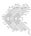
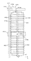
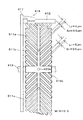
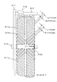
図3は本発明の第1の実施形態の液晶表示装置の平面図、図4は同じくその液晶表示装置の模式断面図である。なお、図3では、2画素分の領域を示している。
次に、赤色感光性樹脂、緑色感光性樹脂及び青色感光性樹脂を使用して、ガラス基板131の上に赤色、緑色及び青色のカラーフィルタ133を形成する。
図6は本発明の第2の実施形態の液晶表示装置を示す平面図である。なお、図6において、図3と同一物には同一符号を付してその詳しい説明は省略する。
図7は本発明の第3の実施形態の液晶表示装置を示す平面図である。図7において、図3と同一物には同一符号を付してその詳しい説明は省略する。
図8は、本発明の第4の実施形態の液晶表示装置を示す平面図である。
図9は、本発明の第5の実施形態の液晶表示装置を示す平面図である。本実施形態が第4の実施形態と異なる点は副画素電極の形状が異なることにあり、その他の構造は第4の実施形態と同様であるので、図9において図8と同一物には同一符号を付してその詳しい説明は省略する。
以下、本発明の第6の実施形態について説明する。

図1に示すような画素電極を有する液晶表示装置を製造した。この比較例1の液晶表示装置の液晶層の厚さdは3.8μm、微細電極部の幅Lは3μm、スリット幅Sは3.5μmである。L+d−Sの値は3.3μmとなり、前述の(1)式を満足していない。この比較例1の液晶表示装置の全面に中間階調の表示を行ったところ、タイル状のパターンが観察された。
図1に示すような画素電極を有する液晶表示装置を製造した。この比較例2の液晶表示装置の液晶層の厚さdは4μm、微細電極部の幅Lは3μm、スリット幅Sは3.5μmである。L+d−Sの値は3.5μmとなり、前述の(1)式を満足していない。この比較例2の液晶表示装置の全面に中間階調の表示を行ったところ、タイル状のパターンが観察された。
図1に示すような画素電極を有する液晶表示装置を製造した。この比較例3の液晶表示装置の液晶層の厚さdは4μm、微細電極部の幅Lは6μm、スリット幅Sは3.5μmである。L+d−Sの値は6.5μmとなり、前述の(1)式を満足する。この比較例3の液晶表示装置の全面に中間階調の表示を行ったところ、タイル状のパターンは観察されなかった。しかしながら、この液晶表示装置の白表示時の輝度を測定したところ、比較例2の液晶表示装置に比べて約10%低下していることが判明した。
図11に示すような画素電極を有する液晶表示装置を製造した。この実施例1の液晶表示装置の液晶層の厚さdは4μm、微細電極部の幅Lは6μm、スリット幅Sは3μmである。L+d−Sの値は7μmとなり、前述の(1)式を満足する。この実施例1の液晶表示装置の全面に中間階調の表示を行ったところ、タイル状のパターンは観察されなかった。また、この液晶表示装置の白表示時の輝度を測定したところ、比較例3の液晶表示装置に比べて約7%向上していることが判明した。
図12に示すような画素電極を有する液晶表示装置を製造した。この実施例2の液晶表示装置の液晶層の厚さdは4μm、微細電極部の幅Lは6μm、スリット幅Sは3μmである。L+d−Sの値は7μmとなり、前述の(1)式を満足する。この実施例2の液晶表示装置の全面に中間階調の表示を行ったところ、タイル状のパターンは観察されなかった。また、この液晶表示装置の白表示時の輝度を測定したところ、比較例3の液晶表示装置に比べて約7.1%向上していることが判明した。
図13に示すような画素電極を有する液晶表示装置を製造した。この実施例3の液晶表示装置の液晶層の厚さdは4μm、微細電極部の幅Lは6μm、スリット幅Sは3μmである。L+d−Sの値は7μmとなり、前述の(1)式を満足する。この実施例3の液晶表示装置の全面に中間階調の表示を行ったところ、タイル状のパターンは観察されなかった。また、この液晶表示装置の白表示時の輝度を測定したところ、比較例3の液晶表示装置に比べて約7.1%向上していることが判明した。
以下、本発明の第7の実施形態について説明する。
以下、本発明の第8の実施形態について説明する。
図21は、本発明の第9の実施形態の液晶表示装置の1画素を示す平面図である。図21において、図18と同一物には同一符号を付してその詳しい説明は省略する。
以下、本発明の第10の実施形態について説明する。
図26は、第10の実施形態の実施例1に係る液晶表示装置の1画素を示す平面図である。
図27は、第10の実施形態の実施例2に係る液晶表示装置の1画素を示す平面図である。なお、実施例2の液晶表示装置が図26に示す実施例1の液晶表示装置と異なる点は、画素電極に設けられたスリットの形状が異なることにあり、その他の構成は基本的に実施例1の液晶表示装置と同様であるので、図27において図26と同一物には同一符号を付してその詳しい説明は省略する。
図28は、第10の実施形態の実施例3に係る液晶表示装置の1画素を示す平面図である。なお、実施例3の液晶表示装置が図26に示す実施例1の液晶表示装置と異なる点は、画素電極に設けられたスリットの形状が異なることにあり、その他の構成は基本的に実施例1の液晶表示装置と同様であるので、図28において図26と同一物には同一符号を付してその詳しい説明は省略する。
図29は、第10の実施形態の実施例4に係る液晶表示装置の1画素を示す平面図である。なお、実施例4の液晶表示装置が図26に示す実施例1の液晶表示装置と異なる点は、画素電極に設けられたスリットの形状が異なることにあり、その他の構成は基本的に実施例1の液晶表示装置と同様であるので、図29において図26と同一物には同一符号を付してその詳しい説明は省略する。
前述したように、1画素内にTFTと直結した副画素電極(直結画素電極)と容量結合を介してTFTに接続した副画素電極(容量結合画素電極)とを形成することにより、斜め方向から見たときの表示品質の劣化を抑制することができる。
前記第1及び第2の基板間に封入された誘電率異方性が負の液晶と、
前記液晶中に添加された重合成分を重合して形成され、電圧印加時に液晶分子の倒れる方向を決定する重合体とを有し、
前記第1の基板には画素毎に、スイッチング素子と、複数の帯状の微細電極部とそれらを相互に電気的に接続する接続電極部とにより構成される第1の副画素電極と、複数の帯状の微細電極部とそれらを相互に電気的に接続する接続電極部とにより構成される第2の副画素電極とが形成され、
前記第2の基板には前記第1及び第2の副画素電極に対向するコモン電極が形成され、
前記第1の副画素電極には前記スイッチング素子を介して第1の電圧が印加され、前記第2の副画素電極には前記第1の電圧よりも低い第2の電圧が印加されることを特徴とする液晶表示装置。
前記第1及び第2の基板間に封入された誘電率異方性が負の液晶と、
前記液晶中に添加された重合成分を重合して形成され、電圧印加時に液晶分子の倒れる方向を決定する重合体とを有し、
前記第1の基板には画素毎に、スイッチング素子と、複数の帯状の微細電極部とそれらを相互に電気的に接続する接続電極部とにより構成される画素電極とが形成され、
前記微細電極部の先端部のうち隣接する微細電極部と対向しない部分に切り欠きを有することを特徴とする液晶表示装置。
前記第1及び第2の基板間に封入された誘電率異方性が負の液晶と、
前記液晶中に添加された重合成分を重合して形成され、電圧印加時に液晶分子の倒れる方向を決定する重合体とを有し、
前記第1の基板には画素毎に、スイッチング素子と、複数の帯状の微細電極部とそれらを相互に電気的に接続する接続電極部とにより構成される画素電極とが形成され、
前記微細電極部の基端側の微細電極部間の領域の形状が、前記微細電極部間の領域の中心線に対し線対称となる形状であることを特徴とする液晶表示装置。
前記第1及び第2の基板間に封入された誘電率異方性が負の液晶と、
前記液晶中に添加された重合成分を重合して形成され、電圧印加時に液晶分子の倒れる方向を決定する重合体とを有し、
前記第1の基板には画素毎に、スイッチング素子と、複数の帯状の微細電極部とそれらを相互に電気的に接続する接続電極部とにより構成される画素電極とが形成され、
前記微細電極部の先端部のうち隣接する微細電極部と対向しない部分に切り欠きを有し、且つ前記微細電極部の基端側の微細電極部間の領域の形状が、前記微細電極部間の領域の中心線に対し線対称となる形状であることを特徴とする液晶表示装置。
前記第1及び第2の基板間に封入された液晶と、
前記液晶中に添加された重合成分を重合して形成され、電圧印加時に液晶分子の倒れる方向を決定する重合体とを有し、
前記第1の基板上には、
一方向に伸びるゲートバスラインと、
前記ゲートバスラインに交差する方向に伸びるデータバスラインと、
前記ゲートバスラインに並行する補助容量バスラインと、
前記ゲートバスライン及び前記データバスラインにより区画される画素領域毎に形成されたスイッチング素子と、
複数の帯状の微細電極部とそれらを相互に電気的に接続する接続電極部とにより構成され、液晶分子の配向方向が相互に異なる複数のドメイン制御領域を有し、前記第1のスイッチング素子に直結された第1の副画素電極と、
前記第1の副画素電極と同一の画素領域内に配置され、複数の帯状の微細電極部とそれらを相互に電気的に接続する接続電極部とにより構成され、液晶分子の配向方向が相互に異なる複数のドメイン制御領域を有する第2の副画素電極と、
第1の絶縁膜を挟んで前記補助容量バスラインに対向する位置に配置された補助容量電極と、
前記スイッチング素子に接続され、前記第1及び第2の副画素電極のドメイン制御領域の境界部に対向する位置に配置されて、第2の絶縁膜を介して前記第2の副画素電極に容量結合する制御電極と、
前記補助容量バスラインに接続され、前記第1の絶縁膜を挟んで前記制御電極に対向する位置に配置された補助容量下部電極とを具備し、
前記第2の基板には前記第1及び第2の副画素電極に対向するコモン電極が形成されていることを特徴とする液晶表示装置。
前記第1及び第2の基板間に封入された誘電率異方性が負の液晶と、
前記液晶中に添加された重合成分を重合して形成され、電圧印加時に液晶分子の倒れる方向を決定する重合体とを有し、
前記第1の基板には画素毎に、スイッチング素子と、液晶分子の配向方向が相互に異なる複数の領域に分割された画素電極とが形成され、
前記画素電極は各領域毎に形成された複数の帯状の微細電極部とそれらを相互に電気的に接続する接続電極部とにより構成され、前記微細電極部の画素縁部の幅が、画素中央側の幅よりも広いことを特徴とする液晶表示装置。
前記第1及び第2の基板間に封入された誘電率異方性が負の液晶と、
前記液晶中に添加された重合成分を重合して形成され、電圧印加時に液晶分子の倒れる方向を決定する重合体とを有し、
前記第1の基板には画素毎に、スイッチング素子と、液晶分子の配向方向が相互に異なる複数の領域に分割された画素電極とが形成され、
前記画素電極には前記領域毎にその伸びる方向が相互に異なる2以上の微細電極部が設けられていることを特徴とする液晶表示装置。
前記第1及び第2の基板間に封入された誘電率異方性が負の液晶と、
前記液晶中に添加された重合成分を重合して形成され、電圧印加時に液晶分子の倒れる方向を決定する重合体とを有し、
前記第1の基板には画素毎に、スイッチング素子と、液晶分子の配向方向が相互に異なる複数の領域に分割された画素電極とが形成され、
前記画素電極は、データバスラインに直交する方向に伸びる複数の微細電極部により構成されていることを特徴とする液晶表示装置。
前記第1及び第2の基板間に封入された誘電率異方性が負の液晶と、
前記液晶中に添加された重合成分を重合して形成され、電圧印加時に液晶分子の倒れる方向を決定する重合体とを有し、
前記第1の基板には画素毎に、スイッチング素子と、液晶分子の配向方向が相互に異なる複数の領域に分割された第1及び第2の副画素電極とが形成され、
前記第1の副画素電極は、各領域毎に所定の方向に伸びる複数の帯状の微細電極部とそれらを相互に電気的に接続する接続電極部とより構成され、前記スイッチング素子に直結されており、
前記第2の副画素電極は、各領域毎に所定の方向に伸びる複数の帯状の微細電極部とそれらを相互に電気的に接続する接続電極部とにより構成され、容量結合を介して前記スイッチング素子に接続されており、
前記第1の副画素電極の微細電極部の幅が前記第2の副画素電極の微細電極部の幅よりも広いことを特徴とする液晶表示装置。
前記第1及び第2の基板間に封入された誘電率異方性が負の液晶と、
前記液晶中に添加された重合成分を重合して形成され、電圧印加時に液晶分子の倒れる方向を決定する重合体とを有し、
前記第1の基板には画素毎に、スイッチング素子と、液晶分子の配向方向が相互に異なる複数の領域に分割された第1及び第2の副画素電極とが形成され、
前記第1の副画素電極は、各領域毎に所定の方向に伸びる複数の帯状の微細電極部とそれらを相互に電気的に接続する接続電極部とにより構成され、前記スイッチング素子に直結されており、
前記第2の副画素電極は、各領域毎に所定の方向に伸びる複数の帯状の微細電極部とそれらを相互に電気的に接続する接続電極部とにより構成され、容量結合を介して前記スイッチング素子に接続されており、
前記第1の副画素電極と前記第2の副画素電極との総面積に対する前記第1の副画素電極の面積比率が10乃至70%であることを特徴とする液晶表示装置。
2,313a,313c,341…補助容量下部電極、
4,119a,119c,151a,151c,161a,161c,171,313a,313c,319a,319c,345,419a…制御電極、
11,112,211,312,412…ゲートバスライン、
12,117,177,202,212,317,417…データバスライン、
14,118,214,318,418…TFT、
15,215,421,441,451,461…画素電極、
110,310…TFT基板、
111,131,311,331…ガラス基板、
113,313,413…補助容量バスライン、
114,120,314,320…絶縁膜、
115,315…半導体膜、
116,316…チャネル保護膜、
119b,151b,161b,313b、319b,419c…補助容量電極
122,153,163,173,183,204,215a,322,422a〜422k.422m,422,452a〜452h,462a〜462d…スリット、
130,330…対向基板、
132,332…ブラックマトリクス、
133,333…カラーフィルタ、
134,334…コモン電極、
140,340…液晶層、
141a,141b…偏光板、
201,215b…微細電極部、
205…接続電極部、
511b…直結画素電極(副画素電極)、
511a,511c…容量結合画素電極(副画素電極)。
Claims (4)
- 相互に対向して配置された第1及び第2の基板と、
前記第1及び第2の基板間に封入された誘電率異方性が負の液晶と、
前記液晶中に添加された重合成分を重合して形成され、電圧印加時に液晶分子の倒れる方向を決定する重合体とを有し、
前記第1の基板には画素毎に、スイッチング素子と、複数の帯状の微細電極部とそれらを相互に電気的に接続する接続電極部とにより構成される第1の副画素電極と、複数の帯状の微細電極部とそれらを相互に電気的に接続する接続電極部とにより構成される第2の副画素電極と、補助容量電極とが形成され、
前記第2の基板には前記第1及び第2の副画素電極に対向するコモン電極が形成され、
前記第1の副画素電極がドメイン制御領域の境界部分に配置されたコンタクトホールを介して前記補助容量電極に接続され、
前記第1の副画素電極には前記スイッチング素子を介して第1の電圧が印加され、前記第2の副画素電極には前記第1の電圧よりも低い第2の電圧が印加されることを特徴とする液晶表示装置。 - 前記第1及び第2の副画素電極の微細電極部の伸びる方向が前記ゲートバスライン及び前記データバスラインのいずれにも交差する方向であり、前記第1及び第2の偏光板のうちの一方の偏光板の吸収軸が前記ゲートバスラインと平行であり、他方の偏光板の吸収軸が前記ゲートバスラインに直交する方向であることを特徴とする請求項1に記載の液晶表示装置。
- 前記データバスラインが、屈曲した形状であることを特徴とする請求項1に記載の液晶表示装置。
- 前記データバスラインの少なくとも一部が、前記微細電極部の伸びる方向に直交する方向に伸びていることを特徴とする請求項1に記載の液晶表示装置。
Priority Applications (14)
| Application Number | Priority Date | Filing Date | Title |
|---|---|---|---|
| JP2005001356A JP4829501B2 (ja) | 2005-01-06 | 2005-01-06 | 液晶表示装置 |
| US11/104,309 US7710523B2 (en) | 2005-01-06 | 2005-04-12 | Liquid crystal display device |
| TW94111659A TWI304902B (en) | 2005-01-06 | 2005-04-13 | Liquid crystal display device |
| KR1020050036249A KR100722914B1 (ko) | 2005-01-06 | 2005-04-29 | 액정 표시 장치 |
| US12/723,977 US8325306B2 (en) | 2005-01-06 | 2010-03-15 | Liquid crystal display device |
| US12/785,215 US7920239B2 (en) | 2005-01-06 | 2010-05-21 | Liquid crystal display device |
| US12/785,248 US7911573B2 (en) | 2005-01-06 | 2010-05-21 | Liquid crystal display device |
| US12/979,060 US8125600B2 (en) | 2005-01-06 | 2010-12-27 | Liquid crystal display device |
| US12/978,822 US7978290B2 (en) | 2005-01-06 | 2010-12-27 | Liquid crystal display device |
| US13/007,894 US8432518B2 (en) | 2005-01-06 | 2011-01-17 | Liquid crystal display device |
| US13/007,908 US8212981B2 (en) | 2005-01-06 | 2011-01-17 | Liquid crystal display device |
| US13/069,640 US8208106B2 (en) | 2005-01-06 | 2011-03-23 | Liquid crystal display device |
| US13/846,563 US8804079B2 (en) | 2005-01-06 | 2013-03-18 | Liquid crystal display device |
| US14/320,190 US9007553B2 (en) | 2005-01-06 | 2014-06-30 | Liquid crystal display device |
Applications Claiming Priority (1)
| Application Number | Priority Date | Filing Date | Title |
|---|---|---|---|
| JP2005001356A JP4829501B2 (ja) | 2005-01-06 | 2005-01-06 | 液晶表示装置 |
Related Child Applications (1)
| Application Number | Title | Priority Date | Filing Date |
|---|---|---|---|
| JP2010003583A Division JP5292320B2 (ja) | 2010-01-12 | 2010-01-12 | 液晶表示装置 |
Publications (2)
| Publication Number | Publication Date |
|---|---|
| JP2006189610A JP2006189610A (ja) | 2006-07-20 |
| JP4829501B2 true JP4829501B2 (ja) | 2011-12-07 |
Family
ID=36639972
Family Applications (1)
| Application Number | Title | Priority Date | Filing Date |
|---|---|---|---|
| JP2005001356A Expired - Fee Related JP4829501B2 (ja) | 2005-01-06 | 2005-01-06 | 液晶表示装置 |
Country Status (4)
| Country | Link |
|---|---|
| US (11) | US7710523B2 (ja) |
| JP (1) | JP4829501B2 (ja) |
| KR (1) | KR100722914B1 (ja) |
| TW (1) | TWI304902B (ja) |
Cited By (1)
| Publication number | Priority date | Publication date | Assignee | Title |
|---|---|---|---|---|
| US10811437B2 (en) | 2018-03-22 | 2020-10-20 | Samsung Display Co., Ltd. | Display device including pixel electrode having multiple domains |
Families Citing this family (153)
| Publication number | Priority date | Publication date | Assignee | Title |
|---|---|---|---|---|
| JP4829501B2 (ja) * | 2005-01-06 | 2011-12-07 | シャープ株式会社 | 液晶表示装置 |
| KR101133761B1 (ko) * | 2005-01-26 | 2012-04-09 | 삼성전자주식회사 | 액정 표시 장치 |
| JP4551230B2 (ja) * | 2005-01-31 | 2010-09-22 | シャープ株式会社 | 液晶表示装置の製造方法 |
| JP4557800B2 (ja) * | 2005-05-24 | 2010-10-06 | シャープ株式会社 | 液晶表示装置 |
| JP2006330605A (ja) * | 2005-05-30 | 2006-12-07 | Sharp Corp | 液晶表示装置 |
| JP4744518B2 (ja) | 2005-06-09 | 2011-08-10 | シャープ株式会社 | 液晶表示装置 |
| KR20070097266A (ko) * | 2006-03-29 | 2007-10-04 | 삼성전자주식회사 | 액정 표시 장치 |
| CN101416105B (zh) | 2006-04-04 | 2011-04-13 | 夏普株式会社 | 液晶显示装置 |
| JP5036354B2 (ja) * | 2006-04-04 | 2012-09-26 | 東京エレクトロン株式会社 | 成膜装置の排気系構造、成膜装置、および排ガスの処理方法 |
| WO2007123244A1 (ja) * | 2006-04-24 | 2007-11-01 | Sharp Kabushiki Kaisha | 液晶表示装置 |
| JP5247008B2 (ja) * | 2006-06-07 | 2013-07-24 | キヤノン株式会社 | 透過型の表示装置 |
| WO2008007583A1 (en) * | 2006-07-14 | 2008-01-17 | Sharp Kabushiki Kaisha | Liquid crystal display device |
| TWI325081B (en) * | 2006-07-31 | 2010-05-21 | Au Optronics Corp | Multi-domain vertical alignment liquid crystal display panel |
| TWI342975B (en) * | 2006-08-08 | 2011-06-01 | Au Optronics Corp | Polymer stabilized alignment lcd panel |
| JP4201051B2 (ja) * | 2006-09-15 | 2008-12-24 | エプソンイメージングデバイス株式会社 | 液晶表示パネル |
| WO2008069181A1 (ja) * | 2006-12-05 | 2008-06-12 | Sharp Kabushiki Kaisha | 液晶表示装置 |
| US8619225B2 (en) * | 2007-03-28 | 2013-12-31 | Japan Display West Inc. | Liquid crystal device with pixel electrode under the common electrode and thinner than drain electrode, method of manufacturing liquid crystal device, and electronic apparatus |
| KR101344874B1 (ko) | 2007-04-30 | 2013-12-26 | 삼성디스플레이 주식회사 | 액정 표시 장치 |
| US7812909B2 (en) | 2007-04-20 | 2010-10-12 | Samsung Electronics Co., Ltd. | Liquid crystal display |
| US8339532B2 (en) * | 2007-06-27 | 2012-12-25 | Sharp Kabushiki Kaisha | Liquid crystal display device |
| KR101469032B1 (ko) * | 2007-06-27 | 2014-12-05 | 삼성디스플레이 주식회사 | 표시 장치 및 그 제조 방법 |
| KR101392887B1 (ko) | 2007-08-01 | 2014-05-09 | 삼성디스플레이 주식회사 | 표시 장치 |
| KR101377007B1 (ko) | 2007-08-14 | 2014-03-26 | 삼성디스플레이 주식회사 | 박막 트랜지스터 어레이 기판 및 이를 포함하는 액정 표시패널 |
| TWI372279B (en) * | 2007-08-28 | 2012-09-11 | Au Optronics Corp | Liquid crystal display panel and pixel structure |
| TWI359303B (en) * | 2007-09-28 | 2012-03-01 | Au Optronics Corp | Liquid crystal display panel |
| CN101398587B (zh) * | 2007-09-29 | 2011-02-16 | 北京京东方光电科技有限公司 | 水平电场型液晶显示装置的像素结构 |
| TWI339304B (en) * | 2007-10-16 | 2011-03-21 | Au Optronics Corp | Pixel structure, driving method thereof and pixel array structure |
| JP4702355B2 (ja) * | 2007-12-06 | 2011-06-15 | ソニー株式会社 | 液晶表示装置の製造方法 |
| WO2009084162A1 (ja) * | 2007-12-28 | 2009-07-09 | Sharp Kabushiki Kaisha | 液晶表示装置 |
| TWI362528B (en) * | 2008-01-02 | 2012-04-21 | Au Optronics Corp | Pixel structure and liquid crystal display having the same |
| US20110001691A1 (en) * | 2008-01-25 | 2011-01-06 | Yoshito Hashimoto | Liquid crystal display device |
| JPWO2009098747A1 (ja) * | 2008-02-04 | 2011-05-26 | シャープ株式会社 | 液晶表示装置 |
| KR20090103461A (ko) | 2008-03-28 | 2009-10-01 | 삼성전자주식회사 | 액정 표시 장치 |
| TWI388909B (zh) * | 2008-06-11 | 2013-03-11 | Chimei Innolux Corp | 薄膜電晶體陣列基板及其應用與製造方法 |
| RU2453880C1 (ru) | 2008-06-20 | 2012-06-20 | Шарп Кабусики Кайся | Жидкокристаллическое устройство отображения |
| TWI371641B (en) * | 2008-06-27 | 2012-09-01 | Au Optronics Corp | Liquid crystal display panel and manufacturing method thereof |
| KR101528758B1 (ko) * | 2008-07-08 | 2015-06-15 | 삼성디스플레이 주식회사 | 액정표시장치의 구동방법, 어레이 기판, 이의 제조방법 및이를 갖는 액정표시장치 |
| KR20100012080A (ko) * | 2008-07-28 | 2010-02-05 | 삼성전자주식회사 | 어레이 기판, 이의 제조방법 및 이를 갖는 액정표시장치 |
| KR101475299B1 (ko) * | 2008-08-20 | 2014-12-23 | 삼성디스플레이 주식회사 | 액정 표시 장치 및 그의 제조 방법 |
| KR101528494B1 (ko) * | 2008-08-27 | 2015-06-12 | 삼성디스플레이 주식회사 | 표시기판, 이를 갖는 액정표시패널 및 이 액정표시패널의 제조 방법 |
| TWI382258B (zh) * | 2008-09-11 | 2013-01-11 | Wintek Corp | 可改善色偏之液晶顯示面板與應用其之液晶顯示裝置 |
| KR101609219B1 (ko) | 2008-10-29 | 2016-04-06 | 삼성디스플레이 주식회사 | 액정표시장치 및 이의 제조방법 |
| KR101518329B1 (ko) | 2008-10-31 | 2015-05-07 | 삼성디스플레이 주식회사 | 액정 표시 장치 |
| CN101740581B (zh) * | 2008-11-26 | 2013-08-14 | 群创光电股份有限公司 | 薄膜晶体管阵列基板及其应用与制造方法 |
| TWI393968B (zh) * | 2008-12-18 | 2013-04-21 | Au Optronics Corp | 液晶顯示面板 |
| KR101576982B1 (ko) | 2008-12-22 | 2015-12-14 | 삼성디스플레이 주식회사 | 액정 표시 장치 |
| KR101629347B1 (ko) | 2008-12-23 | 2016-06-13 | 삼성디스플레이 주식회사 | 어레이 기판 및 이를 갖는 표시장치 |
| KR101613629B1 (ko) | 2009-01-19 | 2016-04-20 | 삼성디스플레이 주식회사 | 액정표시장치와 이의 제조방법 및 이에 포함되는 배향막 조성물 |
| JP5348473B2 (ja) | 2009-01-20 | 2013-11-20 | ソニー株式会社 | 液晶表示装置および電子機器 |
| KR20100085518A (ko) * | 2009-01-21 | 2010-07-29 | 삼성전자주식회사 | 표시기판, 이를 갖는 표시장치 및 표시기판의 제조 방법 |
| EP2397889A4 (en) * | 2009-02-10 | 2013-01-23 | Sharp Kk | LIQUID CRYSTAL DISPLAY DEVICE |
| WO2010100789A1 (ja) | 2009-03-05 | 2010-09-10 | シャープ株式会社 | アクティブマトリクス基板、アクティブマトリクス基板の製造方法、液晶パネル、液晶パネルの製造方法、液晶表示装置、液晶表示ユニット、テレビジョン受像機 |
| WO2010100790A1 (ja) * | 2009-03-05 | 2010-09-10 | シャープ株式会社 | アクティブマトリクス基板、アクティブマトリクス基板の製造方法、液晶パネル、液晶パネルの製造方法、液晶表示装置、液晶表示ユニット、テレビジョン受像機 |
| TWI427383B (zh) * | 2009-03-24 | 2014-02-21 | Au Optronics Corp | 主動陣列基板、液晶顯示面板及其驅動方法 |
| CN103235453B (zh) * | 2009-04-03 | 2016-03-16 | 友达光电股份有限公司 | 像素结构、触控式显示面板以及液晶显示器 |
| WO2010116565A1 (ja) | 2009-04-08 | 2010-10-14 | シャープ株式会社 | 液晶表示装置、液晶表示装置の製造方法、光重合体膜形成用組成物、及び、液晶層形成用組成物 |
| US20120038855A1 (en) * | 2009-04-24 | 2012-02-16 | Sharp Kabushiki Kaisha | Liquid crystal display device |
| WO2010131495A1 (ja) * | 2009-05-13 | 2010-11-18 | シャープ株式会社 | 液晶表示装置及びその製造方法 |
| KR20110014912A (ko) * | 2009-08-06 | 2011-02-14 | 삼성전자주식회사 | 액정 표시 장치 및 그 제조 방법 |
| JP5116879B2 (ja) | 2009-08-24 | 2013-01-09 | シャープ株式会社 | 液晶表示装置 |
| CN102033369A (zh) * | 2009-09-25 | 2011-04-27 | 北京京东方光电科技有限公司 | Ffs型tft-lcd阵列基板的像素结构 |
| CN102231029A (zh) * | 2009-10-09 | 2011-11-02 | 群康科技(深圳)有限公司 | 像素结构、主动组件数组基板与液晶显示面板 |
| TWI406073B (zh) * | 2009-12-11 | 2013-08-21 | Au Optronics Corp | 畫素結構 |
| KR101902984B1 (ko) * | 2010-04-02 | 2018-11-14 | 삼성디스플레이 주식회사 | 화소전극 표시판, 액정표시판 조립체 및 이들을 제조하는 방법들 |
| US9081237B2 (en) | 2010-04-02 | 2015-07-14 | Samsung Display Co., Ltd. | Pixel electrode panel, a liquid crystal display panel assembly and methods for manufacturing the same |
| US9081240B2 (en) | 2010-05-20 | 2015-07-14 | Sharp Kabushiki Kaisha | Liquid crystal display device |
| TWI401502B (zh) * | 2010-06-23 | 2013-07-11 | Au Optronics Corp | 液晶顯示面板 |
| TW201200940A (en) * | 2010-06-30 | 2012-01-01 | Au Optronics Corp | Liquid crystal display panel |
| KR101642346B1 (ko) * | 2010-08-06 | 2016-07-26 | 삼성디스플레이 주식회사 | 표시 기판 및 이를 포함하는 표시 장치 |
| TWI431383B (zh) | 2010-09-01 | 2014-03-21 | Innolux Corp | 畫素陣列基板與液晶顯示裝置 |
| KR101812776B1 (ko) * | 2010-09-27 | 2017-12-28 | 삼성디스플레이 주식회사 | 액정 표시 장치 |
| KR101833498B1 (ko) | 2010-10-29 | 2018-03-02 | 삼성디스플레이 주식회사 | 액정 표시 장치 |
| CN102479792B (zh) * | 2010-11-22 | 2014-02-19 | 群创光电股份有限公司 | 像素阵列基板与液晶显示装置 |
| TWI485495B (zh) * | 2011-01-26 | 2015-05-21 | Innolux Corp | 液晶顯示裝置 |
| WO2012111558A1 (ja) * | 2011-02-15 | 2012-08-23 | シャープ株式会社 | 液晶表示装置 |
| KR101812511B1 (ko) * | 2011-06-07 | 2018-01-31 | 삼성디스플레이 주식회사 | 렌즈 패널, 이의제조 방법 및 이를 갖는 표시 장치 |
| US8928844B2 (en) | 2011-06-09 | 2015-01-06 | Shenzhen China Star Optoelectronics Technology Co., Ltd. | Pixel unit and liquid crystal display panel |
| CN102213886B (zh) * | 2011-06-09 | 2012-12-12 | 深圳市华星光电技术有限公司 | 像素单元与液晶显示面板 |
| CN102236219A (zh) * | 2011-07-01 | 2011-11-09 | 深圳市华星光电技术有限公司 | 一种像素电极及液晶显示面板 |
| CN102236220B (zh) * | 2011-07-07 | 2013-11-06 | 深圳市华星光电技术有限公司 | 像素电极结构 |
| JP5577308B2 (ja) * | 2011-08-25 | 2014-08-20 | 株式会社ジャパンディスプレイ | 液晶表示装置 |
| CN102279492A (zh) * | 2011-08-29 | 2011-12-14 | 深圳市华星光电技术有限公司 | 液晶显示面板及其应用的显示装置 |
| CN102305983A (zh) * | 2011-08-29 | 2012-01-04 | 深圳市华星光电技术有限公司 | 液晶显示面板及其应用的显示装置 |
| WO2013054828A1 (ja) * | 2011-10-11 | 2013-04-18 | シャープ株式会社 | 液晶表示装置 |
| CN102360141B (zh) * | 2011-10-12 | 2014-02-19 | 深圳市华星光电技术有限公司 | 液晶显示面板及其像素电极 |
| CN103091908A (zh) * | 2011-10-27 | 2013-05-08 | 群康科技(深圳)有限公司 | 电极图样、画素布局方法及液晶显示器 |
| TWI452559B (zh) * | 2011-11-14 | 2014-09-11 | Au Optronics Corp | 顯示面板及其驅動方法 |
| US20150009459A1 (en) * | 2011-12-26 | 2015-01-08 | Sharp Kabushiki Kaisha | Liquid crystal display panel and liquid crystal display device |
| KR101941547B1 (ko) * | 2012-01-06 | 2019-04-15 | 삼성디스플레이 주식회사 | 광 배향 방법, 이를 수행하기 위한 노광 장치 및 액정 표시 패널 |
| KR101960459B1 (ko) * | 2012-01-26 | 2019-03-21 | 삼성디스플레이 주식회사 | 액정 표시 장치 |
| US9195101B2 (en) | 2012-03-08 | 2015-11-24 | Sharp Kabushiki Kaisha | Liquid crystal display panel comprising a pixel electrode that includes one uniformly planar electrode region and one or more finely patterned electrode regions |
| TWI472860B (zh) * | 2012-05-07 | 2015-02-11 | Au Optronics Corp | 顯示面板 |
| CN102681271A (zh) * | 2012-05-24 | 2012-09-19 | 深圳市华星光电技术有限公司 | 液晶显示面板及其应用的显示装置 |
| CN102681272A (zh) * | 2012-05-24 | 2012-09-19 | 深圳市华星光电技术有限公司 | 液晶显示面板及其应用的显示装置 |
| CN102722055B (zh) * | 2012-06-04 | 2015-06-17 | 深圳市华星光电技术有限公司 | 阵列基板及液晶显示装置 |
| CN103513472A (zh) * | 2012-06-26 | 2014-01-15 | 群康科技(深圳)有限公司 | 基板、具有其的显示装置及其制造方法 |
| US20140022501A1 (en) * | 2012-07-17 | 2014-01-23 | Shenzhen China Star Optoelectronics Technology Co., Ltd. | Liquid crystal display panel and display apparatus using the same |
| KR101931699B1 (ko) * | 2012-08-07 | 2018-12-24 | 삼성디스플레이 주식회사 | 액정 표시 장치 |
| CN105074552B (zh) * | 2012-12-27 | 2018-01-02 | 凸版印刷株式会社 | 液晶显示装置、液晶显示装置用基板及液晶显示装置用基板的制造方法 |
| JP6093575B2 (ja) | 2013-01-15 | 2017-03-08 | 株式会社ジャパンディスプレイ | 液晶表示装置 |
| KR20140111870A (ko) * | 2013-03-12 | 2014-09-22 | 삼성디스플레이 주식회사 | 액정 표시 장치 |
| JP6124668B2 (ja) * | 2013-04-26 | 2017-05-10 | 三菱電機株式会社 | 薄膜トランジスタ基板およびその製造方法 |
| KR102070436B1 (ko) | 2013-07-02 | 2020-01-29 | 삼성디스플레이 주식회사 | 액정 표시 장치 |
| US10712596B2 (en) * | 2013-08-02 | 2020-07-14 | Samsung Display Co., Ltd. | Liquid crystal display |
| CN103454816B (zh) * | 2013-08-09 | 2016-03-30 | 深圳市华星光电技术有限公司 | 一种液晶显示面板 |
| KR102076758B1 (ko) | 2013-08-12 | 2020-02-13 | 삼성디스플레이 주식회사 | 액정 표시 장치 |
| TWI505004B (zh) | 2013-09-12 | 2015-10-21 | Au Optronics Corp | 畫素結構 |
| KR102108505B1 (ko) | 2013-10-23 | 2020-05-08 | 삼성디스플레이 주식회사 | 박막 트랜지스터 표시판 및 액정 표시 장치 |
| KR102132778B1 (ko) | 2013-10-25 | 2020-07-13 | 삼성디스플레이 주식회사 | 액정 표시 장치 |
| KR102160112B1 (ko) | 2014-03-06 | 2020-09-28 | 삼성디스플레이 주식회사 | 액정 표시 장치 |
| KR20160000933A (ko) * | 2014-06-25 | 2016-01-06 | 삼성디스플레이 주식회사 | 액정 표시 장치 |
| KR102204757B1 (ko) * | 2014-07-09 | 2021-01-19 | 삼성디스플레이 주식회사 | 액정 표시 장치 |
| KR102242084B1 (ko) * | 2014-09-16 | 2021-04-21 | 삼성디스플레이 주식회사 | 곡면 표시 장치 |
| CN104503169B (zh) * | 2014-11-21 | 2018-03-06 | 深圳市华星光电技术有限公司 | 垂直配向型液晶显示器 |
| CN104516162B (zh) * | 2014-12-16 | 2017-01-25 | 南京中电熊猫液晶显示科技有限公司 | 一种垂直配向型液晶显示面板 |
| CN104460134B (zh) * | 2014-12-18 | 2017-12-01 | 深圳市华星光电半导体显示技术有限公司 | 像素电极与液晶显示器 |
| KR101635954B1 (ko) * | 2014-12-31 | 2016-07-07 | 삼성디스플레이 주식회사 | 액정 표시 장치 |
| TWI550320B (zh) * | 2014-12-31 | 2016-09-21 | 友達光電股份有限公司 | 畫素結構 |
| KR102303604B1 (ko) * | 2015-02-17 | 2021-09-17 | 삼성디스플레이 주식회사 | 액정 표시 장치 |
| KR102317719B1 (ko) | 2015-02-23 | 2021-10-26 | 삼성디스플레이 주식회사 | 액정 표시 장치 |
| CN204496141U (zh) * | 2015-03-04 | 2015-07-22 | 京东方科技集团股份有限公司 | 液晶屏及显示装置 |
| KR20160113379A (ko) * | 2015-03-18 | 2016-09-29 | 삼성디스플레이 주식회사 | 곡면 표시 장치 |
| KR20160116099A (ko) * | 2015-03-25 | 2016-10-07 | 삼성디스플레이 주식회사 | 액정 표시 장치 |
| TWI567461B (zh) * | 2015-03-31 | 2017-01-21 | 友達光電股份有限公司 | 畫素結構以及包括此畫素結構的液晶顯示器 |
| KR102438493B1 (ko) * | 2015-06-26 | 2022-08-31 | 삼성디스플레이 주식회사 | 액정 표시 장치 |
| TWI599829B (zh) * | 2015-08-24 | 2017-09-21 | 友達光電股份有限公司 | 畫素結構及彎曲顯示器 |
| CN108027539B (zh) * | 2015-10-02 | 2021-05-04 | 夏普株式会社 | 液晶显示面板及其制造方法 |
| CN105116646B (zh) * | 2015-10-15 | 2019-01-29 | 深圳市华星光电技术有限公司 | 一种电极结构以及液晶显示面板 |
| CN108351557B (zh) * | 2015-10-30 | 2021-08-10 | 夏普株式会社 | 液晶显示面板 |
| CN105467697A (zh) * | 2016-01-20 | 2016-04-06 | 京东方科技集团股份有限公司 | 一种像素结构、显示面板及显示装置 |
| CN115808825A (zh) * | 2016-03-15 | 2023-03-17 | 株式会社半导体能源研究所 | 显示装置、模块及电子设备 |
| TWI581043B (zh) * | 2016-10-04 | 2017-05-01 | 友達光電股份有限公司 | 畫素結構 |
| TWI632537B (zh) * | 2017-08-25 | 2018-08-11 | 友達光電股份有限公司 | 液晶顯示面板 |
| CN108008566A (zh) * | 2017-12-07 | 2018-05-08 | 深圳市华星光电技术有限公司 | 一种液晶显示面板 |
| US11259880B1 (en) | 2018-01-25 | 2022-03-01 | Integrity Implants Inc. | Guiding the trajectory of a second surgical device |
| CN109283755B (zh) * | 2018-08-15 | 2022-01-04 | 咸阳彩虹光电科技有限公司 | 一种像素结构、像素单元及显示面板 |
| US11221522B2 (en) * | 2018-08-24 | 2022-01-11 | Sharp Kabushiki Kaisha | Liquid crystal panel |
| CN110967854A (zh) | 2018-09-28 | 2020-04-07 | 夏普株式会社 | 液晶面板 |
| CN109212844A (zh) * | 2018-10-10 | 2019-01-15 | 深圳市华星光电技术有限公司 | 液晶显示面板及装置 |
| CN109581760A (zh) * | 2018-12-25 | 2019-04-05 | 惠科股份有限公司 | 一种像素电极结构、光掩模和显示面板 |
| US10877323B2 (en) * | 2019-02-12 | 2020-12-29 | Shenzhen China Star Optoelectronics Semiconductor Display Technology Co., Ltd. | Pixel electrode |
| CN109765718A (zh) * | 2019-03-26 | 2019-05-17 | 京东方科技集团股份有限公司 | 一种调光膜的制备方法及调光膜 |
| CN112782881B (zh) * | 2019-11-07 | 2022-11-04 | 咸阳彩虹光电科技有限公司 | 一种像素单元、显示面板及显示装置 |
| CN111338134A (zh) | 2020-03-13 | 2020-06-26 | Tcl华星光电技术有限公司 | 一种像素电极结构及液晶显示面板 |
| CN111399288B (zh) * | 2020-04-14 | 2021-07-06 | 深圳市华星光电半导体显示技术有限公司 | 像素电极及具有该像素电极的液晶显示面板 |
| CN111413829A (zh) * | 2020-04-26 | 2020-07-14 | Tcl华星光电技术有限公司 | 显示面板及显示装置 |
| TWI730829B (zh) * | 2020-06-29 | 2021-06-11 | 友達光電股份有限公司 | 液晶顯示面板 |
| CN115023648B (zh) * | 2020-10-23 | 2023-09-29 | 京东方科技集团股份有限公司 | 显示用电极、显示基板和显示装置 |
| KR102958257B1 (ko) * | 2021-01-13 | 2026-04-29 | 보에 테크놀로지 그룹 컴퍼니 리미티드 | 전극 구조, 디스플레이 패널 및 전자 기기 |
| CN114764204A (zh) | 2021-01-13 | 2022-07-19 | 京东方科技集团股份有限公司 | 显示面板及电子设备 |
| JP7744417B2 (ja) | 2021-04-06 | 2025-09-25 | 京東方科技集團股▲ふん▼有限公司 | 画素電極、アレイ基板及び表示装置 |
| WO2022266930A1 (zh) * | 2021-06-24 | 2022-12-29 | 京东方科技集团股份有限公司 | 显示基板及显示装置 |
| WO2023272480A1 (zh) * | 2021-06-29 | 2023-01-05 | 京东方科技集团股份有限公司 | 一种显示基板、显示装置和显示基板的制作方法 |
Family Cites Families (37)
| Publication number | Priority date | Publication date | Assignee | Title |
|---|---|---|---|---|
| US5126865A (en) * | 1990-12-31 | 1992-06-30 | Honeywell Inc. | Liquid crystal display with sub-pixels |
| US5576858A (en) * | 1991-10-14 | 1996-11-19 | Hosiden Corporation | Gray scale LCD control capacitors formed between a control capacitor electrode on one side of an insulating layer and two subpixel electrodes on the other side |
| JP2756206B2 (ja) | 1992-02-19 | 1998-05-25 | シャープ株式会社 | 反射型液晶表示装置及びその製造方法 |
| US5777700A (en) * | 1993-07-14 | 1998-07-07 | Nec Corporation | Liquid crystal display with improved viewing angle dependence |
| JPH0836186A (ja) | 1994-07-21 | 1996-02-06 | Seiko Epson Corp | 液晶装置の製造方法 |
| JP2768313B2 (ja) * | 1995-06-13 | 1998-06-25 | 日本電気株式会社 | 反射型液晶表示装置 |
| KR100261934B1 (ko) * | 1995-06-16 | 2000-07-15 | 야스카와 히데아키 | 액정표시소자, 그것의 제조방법 및 전자기기 |
| JP3668353B2 (ja) | 1997-02-24 | 2005-07-06 | シャープ株式会社 | 液晶表示装置およびその製造方法 |
| JP4201862B2 (ja) | 1997-02-27 | 2008-12-24 | シャープ株式会社 | 液晶表示装置 |
| JPH1195221A (ja) | 1997-09-22 | 1999-04-09 | Toshiba Corp | 液晶表示素子及びこの液晶表示素子の製造方法 |
| JP2000193938A (ja) | 1998-12-28 | 2000-07-14 | Fujitsu Ltd | 液晶表示装置の駆動方法 |
| KR100635940B1 (ko) * | 1999-10-29 | 2006-10-18 | 삼성전자주식회사 | 수직 배향형 액정 표시 장치 |
| JP2001281690A (ja) | 2000-03-31 | 2001-10-10 | Fujitsu Ltd | 液晶表示装置及びその修復方法 |
| JP3877129B2 (ja) | 2000-09-27 | 2007-02-07 | シャープ株式会社 | 液晶表示装置 |
| JP2002169159A (ja) | 2000-11-27 | 2002-06-14 | Koninkl Philips Electronics Nv | 配向分割型垂直配向液晶表示装置 |
| US6977704B2 (en) | 2001-03-30 | 2005-12-20 | Fujitsu Display Technologies Corporation | Liquid crystal display |
| KR100471397B1 (ko) | 2001-05-31 | 2005-02-21 | 비오이 하이디스 테크놀로지 주식회사 | 프린지 필드 스위칭 액정표시장치 및 그 제조방법 |
| US7113241B2 (en) * | 2001-08-31 | 2006-09-26 | Sharp Kabushiki Kaisha | Liquid crystal display and method of manufacturing the same |
| JP2003156731A (ja) * | 2001-09-07 | 2003-05-30 | Fujitsu Display Technologies Corp | 液晶表示装置及びその製造方法 |
| TW588171B (en) | 2001-10-12 | 2004-05-21 | Fujitsu Display Tech | Liquid crystal display device |
| JP4049589B2 (ja) * | 2002-01-18 | 2008-02-20 | シャープ株式会社 | 液晶表示装置用基板及びそれを備えた液晶表示装置及びその製造方法 |
| JP4169992B2 (ja) * | 2002-02-27 | 2008-10-22 | シャープ株式会社 | 液晶表示装置及びその駆動方法 |
| JP4104885B2 (ja) | 2002-03-18 | 2008-06-18 | シャープ株式会社 | 液晶表示装置及びその製造方法 |
| JP2003315781A (ja) * | 2002-04-19 | 2003-11-06 | Toshiba Corp | 液晶表示装置 |
| KR100840326B1 (ko) * | 2002-06-28 | 2008-06-20 | 삼성전자주식회사 | 액정 표시 장치 및 그에 사용되는 박막 트랜지스터 기판 |
| JP2004077699A (ja) * | 2002-08-14 | 2004-03-11 | Toshiba Corp | 液晶表示装置 |
| KR101071253B1 (ko) * | 2003-05-13 | 2011-10-10 | 삼성전자주식회사 | 다중 도메인 액정 표시 장치 및 그의 박막 트랜지스터표시판 |
| KR20050014414A (ko) * | 2003-07-31 | 2005-02-07 | 삼성전자주식회사 | 다중 도메인 액정 표시 장치 |
| US20050078253A1 (en) * | 2003-08-04 | 2005-04-14 | Hee-Seop Kim | Liquid crystal display and thin film transistor array panel therefor |
| US7206048B2 (en) * | 2003-08-13 | 2007-04-17 | Samsung Electronics Co., Ltd. | Liquid crystal display and panel therefor |
| KR101157223B1 (ko) * | 2003-10-29 | 2012-06-15 | 엘지디스플레이 주식회사 | 횡전계방식 액정표시소자 및 그 제조방법 |
| KR101026810B1 (ko) * | 2003-12-30 | 2011-04-04 | 삼성전자주식회사 | 다중 도메인 액정 표시 장치 |
| JP4459685B2 (ja) * | 2004-03-31 | 2010-04-28 | 富士通株式会社 | 液晶表示装置 |
| JP4361844B2 (ja) * | 2004-07-28 | 2009-11-11 | 富士通株式会社 | 液晶表示装置 |
| JP4829501B2 (ja) * | 2005-01-06 | 2011-12-07 | シャープ株式会社 | 液晶表示装置 |
| KR101219142B1 (ko) * | 2005-02-07 | 2013-01-07 | 삼성디스플레이 주식회사 | 표시장치 및 이의 제조 방법 |
| US7697093B2 (en) | 2006-08-08 | 2010-04-13 | Au Optronics Corp. | Array panel |
-
2005
- 2005-01-06 JP JP2005001356A patent/JP4829501B2/ja not_active Expired - Fee Related
- 2005-04-12 US US11/104,309 patent/US7710523B2/en active Active
- 2005-04-13 TW TW94111659A patent/TWI304902B/zh not_active IP Right Cessation
- 2005-04-29 KR KR1020050036249A patent/KR100722914B1/ko not_active Expired - Fee Related
-
2010
- 2010-03-15 US US12/723,977 patent/US8325306B2/en not_active Expired - Fee Related
- 2010-05-21 US US12/785,248 patent/US7911573B2/en not_active Expired - Lifetime
- 2010-05-21 US US12/785,215 patent/US7920239B2/en not_active Expired - Lifetime
- 2010-12-27 US US12/979,060 patent/US8125600B2/en not_active Expired - Lifetime
- 2010-12-27 US US12/978,822 patent/US7978290B2/en not_active Expired - Fee Related
-
2011
- 2011-01-17 US US13/007,908 patent/US8212981B2/en not_active Expired - Lifetime
- 2011-01-17 US US13/007,894 patent/US8432518B2/en not_active Expired - Fee Related
- 2011-03-23 US US13/069,640 patent/US8208106B2/en not_active Expired - Lifetime
-
2013
- 2013-03-18 US US13/846,563 patent/US8804079B2/en not_active Expired - Lifetime
-
2014
- 2014-06-30 US US14/320,190 patent/US9007553B2/en not_active Expired - Lifetime
Cited By (1)
| Publication number | Priority date | Publication date | Assignee | Title |
|---|---|---|---|---|
| US10811437B2 (en) | 2018-03-22 | 2020-10-20 | Samsung Display Co., Ltd. | Display device including pixel electrode having multiple domains |
Also Published As
| Publication number | Publication date |
|---|---|
| US8125600B2 (en) | 2012-02-28 |
| US20100165259A1 (en) | 2010-07-01 |
| US20130208202A1 (en) | 2013-08-15 |
| US7710523B2 (en) | 2010-05-04 |
| US8212981B2 (en) | 2012-07-03 |
| US20100265448A1 (en) | 2010-10-21 |
| US20060146243A1 (en) | 2006-07-06 |
| US8804079B2 (en) | 2014-08-12 |
| US8208106B2 (en) | 2012-06-26 |
| US8432518B2 (en) | 2013-04-30 |
| KR100722914B1 (ko) | 2007-05-30 |
| TWI304902B (en) | 2009-01-01 |
| TW200624917A (en) | 2006-07-16 |
| US8325306B2 (en) | 2012-12-04 |
| US20140313449A1 (en) | 2014-10-23 |
| US20110109826A1 (en) | 2011-05-12 |
| US20110170027A1 (en) | 2011-07-14 |
| US7920239B2 (en) | 2011-04-05 |
| US20110090448A1 (en) | 2011-04-21 |
| US7978290B2 (en) | 2011-07-12 |
| KR20060080843A (ko) | 2006-07-11 |
| US20110090449A1 (en) | 2011-04-21 |
| US9007553B2 (en) | 2015-04-14 |
| US7911573B2 (en) | 2011-03-22 |
| JP2006189610A (ja) | 2006-07-20 |
| US20110109860A1 (en) | 2011-05-12 |
| US20110001913A1 (en) | 2011-01-06 |
Similar Documents
| Publication | Publication Date | Title |
|---|---|---|
| KR100722914B1 (ko) | 액정 표시 장치 | |
| US7570332B2 (en) | Liquid crystal displays having multi-domains and a manufacturing method thereof | |
| JP4436161B2 (ja) | 液晶表示装置 | |
| US20050078253A1 (en) | Liquid crystal display and thin film transistor array panel therefor | |
| JP5554822B2 (ja) | 液晶表示装置 | |
| JP5292320B2 (ja) | 液晶表示装置 | |
| US7499131B2 (en) | Liquid crystal display device with different alignments | |
| KR20060084383A (ko) | 액정 표시 장치 | |
| JP4551230B2 (ja) | 液晶表示装置の製造方法 | |
| JP4447484B2 (ja) | 液晶表示装置 | |
| JP4995942B2 (ja) | 液晶表示装置 | |
| KR100768382B1 (ko) | 액정 표시 장치 | |
| JP2006267689A (ja) | 液晶表示装置の製造方法、及び液晶表示装置 | |
| KR100750015B1 (ko) | 멀티-도메인 수직 정렬 액정표시장치 | |
| JP2009294402A (ja) | 液晶表示装置 | |
| KR20050081319A (ko) | 액정 표시 장치 |
Legal Events
| Date | Code | Title | Description |
|---|---|---|---|
| A621 | Written request for application examination |
Free format text: JAPANESE INTERMEDIATE CODE: A621 Effective date: 20070302 |
|
| A977 | Report on retrieval |
Free format text: JAPANESE INTERMEDIATE CODE: A971007 Effective date: 20090930 |
|
| A131 | Notification of reasons for refusal |
Free format text: JAPANESE INTERMEDIATE CODE: A131 Effective date: 20091110 |
|
| A521 | Request for written amendment filed |
Free format text: JAPANESE INTERMEDIATE CODE: A523 Effective date: 20100112 |
|
| A131 | Notification of reasons for refusal |
Free format text: JAPANESE INTERMEDIATE CODE: A131 Effective date: 20100706 |
|
| A521 | Request for written amendment filed |
Free format text: JAPANESE INTERMEDIATE CODE: A523 Effective date: 20100903 |
|
| A131 | Notification of reasons for refusal |
Free format text: JAPANESE INTERMEDIATE CODE: A131 Effective date: 20110301 |
|
| A521 | Request for written amendment filed |
Free format text: JAPANESE INTERMEDIATE CODE: A523 Effective date: 20110428 |
|
| TRDD | Decision of grant or rejection written | ||
| A01 | Written decision to grant a patent or to grant a registration (utility model) |
Free format text: JAPANESE INTERMEDIATE CODE: A01 Effective date: 20110913 |
|
| A01 | Written decision to grant a patent or to grant a registration (utility model) |
Free format text: JAPANESE INTERMEDIATE CODE: A01 |
|
| A61 | First payment of annual fees (during grant procedure) |
Free format text: JAPANESE INTERMEDIATE CODE: A61 Effective date: 20110916 |
|
| FPAY | Renewal fee payment (event date is renewal date of database) |
Free format text: PAYMENT UNTIL: 20140922 Year of fee payment: 3 |
|
| R150 | Certificate of patent or registration of utility model |
Ref document number: 4829501 Country of ref document: JP Free format text: JAPANESE INTERMEDIATE CODE: R150 Free format text: JAPANESE INTERMEDIATE CODE: R150 |
|
| LAPS | Cancellation because of no payment of annual fees |