JP4843229B2 - 半導体装置の製造方法 - Google Patents
半導体装置の製造方法 Download PDFInfo
- Publication number
- JP4843229B2 JP4843229B2 JP2005047679A JP2005047679A JP4843229B2 JP 4843229 B2 JP4843229 B2 JP 4843229B2 JP 2005047679 A JP2005047679 A JP 2005047679A JP 2005047679 A JP2005047679 A JP 2005047679A JP 4843229 B2 JP4843229 B2 JP 4843229B2
- Authority
- JP
- Japan
- Prior art keywords
- plating film
- opening
- film
- plating
- forming
- Prior art date
- Legal status (The legal status is an assumption and is not a legal conclusion. Google has not performed a legal analysis and makes no representation as to the accuracy of the status listed.)
- Expired - Fee Related
Links
Images



Classifications
-
- H—ELECTRICITY
- H10—SEMICONDUCTOR DEVICES; ELECTRIC SOLID-STATE DEVICES NOT OTHERWISE PROVIDED FOR
- H10W—GENERIC PACKAGES, INTERCONNECTIONS, CONNECTORS OR OTHER CONSTRUCTIONAL DETAILS OF DEVICES COVERED BY CLASS H10
- H10W72/00—Interconnections or connectors in packages
- H10W72/20—Bump connectors, e.g. solder bumps or copper pillars; Dummy bumps; Thermal bumps
-
- H—ELECTRICITY
- H10—SEMICONDUCTOR DEVICES; ELECTRIC SOLID-STATE DEVICES NOT OTHERWISE PROVIDED FOR
- H10W—GENERIC PACKAGES, INTERCONNECTIONS, CONNECTORS OR OTHER CONSTRUCTIONAL DETAILS OF DEVICES COVERED BY CLASS H10
- H10W72/00—Interconnections or connectors in packages
- H10W72/01—Manufacture or treatment
- H10W72/012—Manufacture or treatment of bump connectors, dummy bumps or thermal bumps
-
- H—ELECTRICITY
- H10—SEMICONDUCTOR DEVICES; ELECTRIC SOLID-STATE DEVICES NOT OTHERWISE PROVIDED FOR
- H10W—GENERIC PACKAGES, INTERCONNECTIONS, CONNECTORS OR OTHER CONSTRUCTIONAL DETAILS OF DEVICES COVERED BY CLASS H10
- H10W72/00—Interconnections or connectors in packages
- H10W72/90—Bond pads, in general
-
- H—ELECTRICITY
- H10—SEMICONDUCTOR DEVICES; ELECTRIC SOLID-STATE DEVICES NOT OTHERWISE PROVIDED FOR
- H10W—GENERIC PACKAGES, INTERCONNECTIONS, CONNECTORS OR OTHER CONSTRUCTIONAL DETAILS OF DEVICES COVERED BY CLASS H10
- H10W20/00—Interconnections in chips, wafers or substrates
- H10W20/40—Interconnections external to wafers or substrates, e.g. back-end-of-line [BEOL] metallisations or vias connecting to gate electrodes
- H10W20/49—Adaptable interconnections, e.g. fuses or antifuses
-
- H—ELECTRICITY
- H10—SEMICONDUCTOR DEVICES; ELECTRIC SOLID-STATE DEVICES NOT OTHERWISE PROVIDED FOR
- H10W—GENERIC PACKAGES, INTERCONNECTIONS, CONNECTORS OR OTHER CONSTRUCTIONAL DETAILS OF DEVICES COVERED BY CLASS H10
- H10W70/00—Package substrates; Interposers; Redistribution layers [RDL]
- H10W70/60—Insulating or insulated package substrates; Interposers; Redistribution layers
-
- H—ELECTRICITY
- H10—SEMICONDUCTOR DEVICES; ELECTRIC SOLID-STATE DEVICES NOT OTHERWISE PROVIDED FOR
- H10W—GENERIC PACKAGES, INTERCONNECTIONS, CONNECTORS OR OTHER CONSTRUCTIONAL DETAILS OF DEVICES COVERED BY CLASS H10
- H10W72/00—Interconnections or connectors in packages
- H10W72/01—Manufacture or treatment
- H10W72/012—Manufacture or treatment of bump connectors, dummy bumps or thermal bumps
- H10W72/01231—Manufacture or treatment of bump connectors, dummy bumps or thermal bumps using blanket deposition
- H10W72/01233—Manufacture or treatment of bump connectors, dummy bumps or thermal bumps using blanket deposition in liquid form, e.g. spin coating, spray coating or immersion coating
- H10W72/01235—Manufacture or treatment of bump connectors, dummy bumps or thermal bumps using blanket deposition in liquid form, e.g. spin coating, spray coating or immersion coating by plating, e.g. electroless plating or electroplating
-
- H—ELECTRICITY
- H10—SEMICONDUCTOR DEVICES; ELECTRIC SOLID-STATE DEVICES NOT OTHERWISE PROVIDED FOR
- H10W—GENERIC PACKAGES, INTERCONNECTIONS, CONNECTORS OR OTHER CONSTRUCTIONAL DETAILS OF DEVICES COVERED BY CLASS H10
- H10W72/00—Interconnections or connectors in packages
- H10W72/01—Manufacture or treatment
- H10W72/012—Manufacture or treatment of bump connectors, dummy bumps or thermal bumps
- H10W72/01251—Changing the shapes of bumps
- H10W72/01257—Changing the shapes of bumps by reflowing
-
- H—ELECTRICITY
- H10—SEMICONDUCTOR DEVICES; ELECTRIC SOLID-STATE DEVICES NOT OTHERWISE PROVIDED FOR
- H10W—GENERIC PACKAGES, INTERCONNECTIONS, CONNECTORS OR OTHER CONSTRUCTIONAL DETAILS OF DEVICES COVERED BY CLASS H10
- H10W72/00—Interconnections or connectors in packages
- H10W72/01—Manufacture or treatment
- H10W72/012—Manufacture or treatment of bump connectors, dummy bumps or thermal bumps
- H10W72/01261—Chemical or physical modification, e.g. by sintering or anodisation
-
- H—ELECTRICITY
- H10—SEMICONDUCTOR DEVICES; ELECTRIC SOLID-STATE DEVICES NOT OTHERWISE PROVIDED FOR
- H10W—GENERIC PACKAGES, INTERCONNECTIONS, CONNECTORS OR OTHER CONSTRUCTIONAL DETAILS OF DEVICES COVERED BY CLASS H10
- H10W72/00—Interconnections or connectors in packages
- H10W72/20—Bump connectors, e.g. solder bumps or copper pillars; Dummy bumps; Thermal bumps
- H10W72/251—Materials
-
- H—ELECTRICITY
- H10—SEMICONDUCTOR DEVICES; ELECTRIC SOLID-STATE DEVICES NOT OTHERWISE PROVIDED FOR
- H10W—GENERIC PACKAGES, INTERCONNECTIONS, CONNECTORS OR OTHER CONSTRUCTIONAL DETAILS OF DEVICES COVERED BY CLASS H10
- H10W72/00—Interconnections or connectors in packages
- H10W72/20—Bump connectors, e.g. solder bumps or copper pillars; Dummy bumps; Thermal bumps
- H10W72/251—Materials
- H10W72/252—Materials comprising solid metals or solid metalloids, e.g. PbSn, Ag or Cu
-
- H—ELECTRICITY
- H10—SEMICONDUCTOR DEVICES; ELECTRIC SOLID-STATE DEVICES NOT OTHERWISE PROVIDED FOR
- H10W—GENERIC PACKAGES, INTERCONNECTIONS, CONNECTORS OR OTHER CONSTRUCTIONAL DETAILS OF DEVICES COVERED BY CLASS H10
- H10W72/00—Interconnections or connectors in packages
- H10W72/20—Bump connectors, e.g. solder bumps or copper pillars; Dummy bumps; Thermal bumps
- H10W72/29—Bond pads specially adapted therefor
-
- H—ELECTRICITY
- H10—SEMICONDUCTOR DEVICES; ELECTRIC SOLID-STATE DEVICES NOT OTHERWISE PROVIDED FOR
- H10W—GENERIC PACKAGES, INTERCONNECTIONS, CONNECTORS OR OTHER CONSTRUCTIONAL DETAILS OF DEVICES COVERED BY CLASS H10
- H10W72/00—Interconnections or connectors in packages
- H10W72/90—Bond pads, in general
- H10W72/941—Dispositions of bond pads
- H10W72/9415—Dispositions of bond pads relative to the surface, e.g. recessed, protruding
-
- H—ELECTRICITY
- H10—SEMICONDUCTOR DEVICES; ELECTRIC SOLID-STATE DEVICES NOT OTHERWISE PROVIDED FOR
- H10W—GENERIC PACKAGES, INTERCONNECTIONS, CONNECTORS OR OTHER CONSTRUCTIONAL DETAILS OF DEVICES COVERED BY CLASS H10
- H10W72/00—Interconnections or connectors in packages
- H10W72/90—Bond pads, in general
- H10W72/941—Dispositions of bond pads
- H10W72/942—Dispositions of bond pads relative to underlying supporting features, e.g. bond pads, RDLs or vias
Landscapes
- Internal Circuitry In Semiconductor Integrated Circuit Devices (AREA)
Description
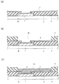
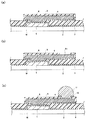
以下、第1の実施の形態について説明する。図1(a)〜図3(b)は本実施の形態に係る半導体装置の製造プロセスの模式図である。
以下、第2の実施の形態について説明する。なお、第1の実施の形態と重複する説明は省略することもある。本実施の形態では、第1の実施の形態で説明した手法を用いてウェハレベルCSP(Chip Scale Package)の再配置配線を形成する例について説明する。図4(a)〜図6(c)は本実施の形態に係る半導体装置の製造プロセスの模式図である。
Claims (2)
- 基板上に通電層を形成する工程と、
所定の位置に開口を有するレジストマスクを前記通電層上に形成する工程と、
前記通電層に電流を供給して、めっき法により前記開口内にめっき膜を形成する工程と、前記開口を形成する前記レジストマスクの内側面を後退させて、前記内側面と前記めっき膜との間隔を広げる工程と、
前記めっき膜を覆うように前記内側面の後退した前記開口内に絶縁膜を形成する工程と、前記レジストマスクを除去する工程と、
前記めっき膜及び前記絶縁膜に覆われている部分以外の前記通電層を除去する工程と、前記絶縁膜に第2の開口を形成する工程と、
前記第2の開口に半田バンプを形成する工程と、
をさらに具備することを特徴とする半導体装置の製造方法。 - 前記めっき膜はCuから構成されており、前記絶縁膜はポリイミドから構成されていることを特徴とする請求項1記載の半導体装置の製造方法
Priority Applications (3)
| Application Number | Priority Date | Filing Date | Title |
|---|---|---|---|
| JP2005047679A JP4843229B2 (ja) | 2005-02-23 | 2005-02-23 | 半導体装置の製造方法 |
| US11/358,137 US7473628B2 (en) | 2005-02-23 | 2006-02-22 | Method of manufacturing semiconductor device and semiconductor device |
| US12/314,135 US20090134516A1 (en) | 2005-02-23 | 2008-12-04 | Method of manufacturing semiconductor device and semiconductor device |
Applications Claiming Priority (1)
| Application Number | Priority Date | Filing Date | Title |
|---|---|---|---|
| JP2005047679A JP4843229B2 (ja) | 2005-02-23 | 2005-02-23 | 半導体装置の製造方法 |
Publications (2)
| Publication Number | Publication Date |
|---|---|
| JP2006237159A JP2006237159A (ja) | 2006-09-07 |
| JP4843229B2 true JP4843229B2 (ja) | 2011-12-21 |
Family
ID=36913307
Family Applications (1)
| Application Number | Title | Priority Date | Filing Date |
|---|---|---|---|
| JP2005047679A Expired - Fee Related JP4843229B2 (ja) | 2005-02-23 | 2005-02-23 | 半導体装置の製造方法 |
Country Status (2)
| Country | Link |
|---|---|
| US (2) | US7473628B2 (ja) |
| JP (1) | JP4843229B2 (ja) |
Families Citing this family (21)
| Publication number | Priority date | Publication date | Assignee | Title |
|---|---|---|---|---|
| JP2009064989A (ja) | 2007-09-07 | 2009-03-26 | Panasonic Corp | 半導体装置およびその製造方法 |
| JP5512082B2 (ja) | 2007-12-17 | 2014-06-04 | 株式会社東芝 | 半導体装置の製造方法及び半導体装置 |
| JP4724192B2 (ja) * | 2008-02-28 | 2011-07-13 | 株式会社東芝 | 電子部品の製造方法 |
| US20100264522A1 (en) * | 2009-04-20 | 2010-10-21 | Chien-Pin Chen | Semiconductor device having at least one bump without overlapping specific pad or directly contacting specific pad |
| JP2011054805A (ja) * | 2009-09-02 | 2011-03-17 | Toshiba Corp | 半導体装置、及び半導体装置の製造方法 |
| US8889995B2 (en) * | 2011-03-03 | 2014-11-18 | Skyworks Solutions, Inc. | Wire bond pad system and method |
| US9679869B2 (en) | 2011-09-02 | 2017-06-13 | Skyworks Solutions, Inc. | Transmission line for high performance radio frequency applications |
| US9589862B2 (en) | 2013-03-11 | 2017-03-07 | Taiwan Semiconductor Manufacturing Company, Ltd. | Interconnect structures and methods of forming same |
| US9607921B2 (en) * | 2012-01-12 | 2017-03-28 | Taiwan Semiconductor Manufacturing Company, Ltd. | Package on package interconnect structure |
| US9257333B2 (en) | 2013-03-11 | 2016-02-09 | Taiwan Semiconductor Manufacturing Company, Ltd. | Interconnect structures and methods of forming same |
| US9368398B2 (en) | 2012-01-12 | 2016-06-14 | Taiwan Semiconductor Manufacturing Company, Ltd. | Interconnect structure and method of fabricating same |
| US10015888B2 (en) | 2013-02-15 | 2018-07-03 | Taiwan Semiconductor Manufacturing Company, Ltd. | Interconnect joint protective layer apparatus and method |
| US9401308B2 (en) | 2013-03-12 | 2016-07-26 | Taiwan Semiconductor Manufacturing Company, Ltd. | Packaging devices, methods of manufacture thereof, and packaging methods |
| US9263839B2 (en) | 2012-12-28 | 2016-02-16 | Taiwan Semiconductor Manufacturing Company, Ltd. | System and method for an improved fine pitch joint |
| US8680959B2 (en) | 2012-05-09 | 2014-03-25 | Hamilton Sundstrand Corporation | Immersion cooled inductor apparatus |
| KR102250612B1 (ko) | 2012-06-14 | 2021-05-10 | 스카이워크스 솔루션즈, 인코포레이티드 | 고조파 종단 회로를 포함하는 전력 증폭기 모듈 및 관련된 시스템, 장치, 및 방법 |
| US9082776B2 (en) | 2012-08-24 | 2015-07-14 | Taiwan Semiconductor Manufacturing Company, Ltd. | Semiconductor package having protective layer with curved surface and method of manufacturing same |
| US9082870B2 (en) * | 2013-03-13 | 2015-07-14 | Taiwan Semiconductor Manufacturing Company, Ltd. | Methods and apparatus of packaging semiconductor devices |
| US9609752B1 (en) * | 2013-03-15 | 2017-03-28 | Lockheed Martin Corporation | Interconnect structure configured to control solder flow and method of manufacturing of same |
| US9892962B2 (en) | 2015-11-30 | 2018-02-13 | Taiwan Semiconductor Manufacturing Company, Ltd. | Wafer level chip scale package interconnects and methods of manufacture thereof |
| CN108796584B (zh) * | 2017-04-28 | 2020-08-25 | 宝山钢铁股份有限公司 | 一种镀锡产品表面钝化膜结构柔性控制方法 |
Family Cites Families (14)
| Publication number | Priority date | Publication date | Assignee | Title |
|---|---|---|---|---|
| US6111317A (en) * | 1996-01-18 | 2000-08-29 | Kabushiki Kaisha Toshiba | Flip-chip connection type semiconductor integrated circuit device |
| JP3561582B2 (ja) * | 1996-09-18 | 2004-09-02 | 沖電気工業株式会社 | 半導体装置の製造方法 |
| US5946590A (en) * | 1996-12-10 | 1999-08-31 | Citizen Watch Co., Ltd. | Method for making bumps |
| KR100219806B1 (ko) * | 1997-05-27 | 1999-09-01 | 윤종용 | 반도체장치의 플립 칩 실장형 솔더 범프의 제조방법, 이에 따라 제조되는 솔더범프 및 그 분석방법 |
| US6642136B1 (en) * | 2001-09-17 | 2003-11-04 | Megic Corporation | Method of making a low fabrication cost, high performance, high reliability chip scale package |
| JP4237325B2 (ja) * | 1999-03-11 | 2009-03-11 | 株式会社東芝 | 半導体素子およびその製造方法 |
| DE60022458T2 (de) * | 1999-06-15 | 2006-06-22 | Fujikura Ltd. | Halbleitergehäuse, halbleitervorrichtung, elektronikelement und herstellung eines halbleitergehäuses |
| KR100313706B1 (ko) * | 1999-09-29 | 2001-11-26 | 윤종용 | 재배치 웨이퍼 레벨 칩 사이즈 패키지 및 그 제조방법 |
| JP4656275B2 (ja) * | 2001-01-15 | 2011-03-23 | 日本電気株式会社 | 半導体装置の製造方法 |
| US6818545B2 (en) * | 2001-03-05 | 2004-11-16 | Megic Corporation | Low fabrication cost, fine pitch and high reliability solder bump |
| US6593220B1 (en) * | 2002-01-03 | 2003-07-15 | Taiwan Semiconductor Manufacturing Company | Elastomer plating mask sealed wafer level package method |
| JP4260405B2 (ja) * | 2002-02-08 | 2009-04-30 | 株式会社ルネサステクノロジ | 半導体集積回路装置の製造方法 |
| US20050242446A1 (en) * | 2002-09-19 | 2005-11-03 | Stats Chippac Ltd. | Integrated circuit package with different hardness bump pad and bump and manufacturing method therefor |
| TWI242866B (en) | 2003-08-21 | 2005-11-01 | Siliconware Precision Industries Co Ltd | Process of forming lead-free bumps on electronic component |
-
2005
- 2005-02-23 JP JP2005047679A patent/JP4843229B2/ja not_active Expired - Fee Related
-
2006
- 2006-02-22 US US11/358,137 patent/US7473628B2/en not_active Expired - Fee Related
-
2008
- 2008-12-04 US US12/314,135 patent/US20090134516A1/en not_active Abandoned
Also Published As
| Publication number | Publication date |
|---|---|
| US20090134516A1 (en) | 2009-05-28 |
| US20060189114A1 (en) | 2006-08-24 |
| US7473628B2 (en) | 2009-01-06 |
| JP2006237159A (ja) | 2006-09-07 |
Similar Documents
| Publication | Publication Date | Title |
|---|---|---|
| JP4843229B2 (ja) | 半導体装置の製造方法 | |
| TWI442532B (zh) | 積體電路元件與封裝組件 | |
| US9685372B2 (en) | Method of forming Cu pillar bump with non-metal sidewall spacer and metal top cap | |
| CN102315182B (zh) | 半导体芯片及其制造方法 | |
| US8241963B2 (en) | Recessed pillar structure | |
| US11257714B2 (en) | Method of making a pillar structure having a non-metal sidewall protection structure and integrated circuit including the same | |
| CN102593044B (zh) | 形成金属柱的方法 | |
| US8569162B2 (en) | Conductive bump structure on substrate and fabrication method thereof | |
| US20140361431A1 (en) | Semiconductor device and manufacturing method thereof | |
| TWI611486B (zh) | 半導體結構及其製法 | |
| CN103325696A (zh) | 晶圆级半导体封装件的制法及其晶圆级封装基板的制法 | |
| US8866293B2 (en) | Semiconductor structure and fabrication method thereof | |
| JP6538596B2 (ja) | 電子部品の製造方法及び電子部品の製造装置 | |
| US20250343199A1 (en) | Electronic device and manufacturing method thereof | |
| CN103681576A (zh) | 具有无源能量元件的半导体封装器件 | |
| US10797010B2 (en) | Semiconductor package having a metal barrier | |
| US9466547B1 (en) | Passivation layer topography | |
| JP2004200420A (ja) | 半導体装置及びその製造方法 | |
| US20240006371A1 (en) | Semiconductor device interconnect structure | |
| JP2009200132A (ja) | 半導体装置及びその製造方法 |
Legal Events
| Date | Code | Title | Description |
|---|---|---|---|
| A621 | Written request for application examination |
Free format text: JAPANESE INTERMEDIATE CODE: A621 Effective date: 20071212 |
|
| A977 | Report on retrieval |
Free format text: JAPANESE INTERMEDIATE CODE: A971007 Effective date: 20100210 |
|
| A131 | Notification of reasons for refusal |
Free format text: JAPANESE INTERMEDIATE CODE: A131 Effective date: 20100914 |
|
| A521 | Request for written amendment filed |
Free format text: JAPANESE INTERMEDIATE CODE: A523 Effective date: 20101115 |
|
| RD02 | Notification of acceptance of power of attorney |
Free format text: JAPANESE INTERMEDIATE CODE: A7422 Effective date: 20101115 |
|
| A02 | Decision of refusal |
Free format text: JAPANESE INTERMEDIATE CODE: A02 Effective date: 20101214 |
|
| A521 | Request for written amendment filed |
Free format text: JAPANESE INTERMEDIATE CODE: A523 Effective date: 20110314 |
|
| A911 | Transfer to examiner for re-examination before appeal (zenchi) |
Free format text: JAPANESE INTERMEDIATE CODE: A911 Effective date: 20110509 |
|
| A131 | Notification of reasons for refusal |
Free format text: JAPANESE INTERMEDIATE CODE: A131 Effective date: 20110617 |
|
| A521 | Request for written amendment filed |
Free format text: JAPANESE INTERMEDIATE CODE: A523 Effective date: 20110729 |
|
| TRDD | Decision of grant or rejection written | ||
| A01 | Written decision to grant a patent or to grant a registration (utility model) |
Free format text: JAPANESE INTERMEDIATE CODE: A01 Effective date: 20110913 |
|
| A01 | Written decision to grant a patent or to grant a registration (utility model) |
Free format text: JAPANESE INTERMEDIATE CODE: A01 |
|
| A61 | First payment of annual fees (during grant procedure) |
Free format text: JAPANESE INTERMEDIATE CODE: A61 Effective date: 20111007 |
|
| FPAY | Renewal fee payment (event date is renewal date of database) |
Free format text: PAYMENT UNTIL: 20141014 Year of fee payment: 3 |
|
| LAPS | Cancellation because of no payment of annual fees |