JP4850423B2 - 窒化物半導体装置 - Google Patents
窒化物半導体装置 Download PDFInfo
- Publication number
- JP4850423B2 JP4850423B2 JP2005039387A JP2005039387A JP4850423B2 JP 4850423 B2 JP4850423 B2 JP 4850423B2 JP 2005039387 A JP2005039387 A JP 2005039387A JP 2005039387 A JP2005039387 A JP 2005039387A JP 4850423 B2 JP4850423 B2 JP 4850423B2
- Authority
- JP
- Japan
- Prior art keywords
- nitride semiconductor
- semiconductor layer
- layer
- electrode
- semiconductor device
- Prior art date
- Legal status (The legal status is an assumption and is not a legal conclusion. Google has not performed a legal analysis and makes no representation as to the accuracy of the status listed.)
- Expired - Fee Related
Links
- 239000004065 semiconductor Substances 0.000 title claims description 108
- 150000004767 nitrides Chemical class 0.000 title claims description 97
- 239000000758 substrate Substances 0.000 claims description 15
- 229910052782 aluminium Inorganic materials 0.000 claims description 10
- XAGFODPZIPBFFR-UHFFFAOYSA-N aluminium Chemical compound [Al] XAGFODPZIPBFFR-UHFFFAOYSA-N 0.000 claims description 10
- IJGRMHOSHXDMSA-UHFFFAOYSA-N Atomic nitrogen Chemical compound N#N IJGRMHOSHXDMSA-UHFFFAOYSA-N 0.000 claims description 8
- 230000015572 biosynthetic process Effects 0.000 claims description 6
- 229910052757 nitrogen Inorganic materials 0.000 claims description 4
- ZOXJGFHDIHLPTG-UHFFFAOYSA-N Boron Chemical compound [B] ZOXJGFHDIHLPTG-UHFFFAOYSA-N 0.000 claims description 2
- GYHNNYVSQQEPJS-UHFFFAOYSA-N Gallium Chemical compound [Ga] GYHNNYVSQQEPJS-UHFFFAOYSA-N 0.000 claims description 2
- OAICVXFJPJFONN-UHFFFAOYSA-N Phosphorus Chemical compound [P] OAICVXFJPJFONN-UHFFFAOYSA-N 0.000 claims description 2
- 229910052785 arsenic Inorganic materials 0.000 claims description 2
- RQNWIZPPADIBDY-UHFFFAOYSA-N arsenic atom Chemical compound [As] RQNWIZPPADIBDY-UHFFFAOYSA-N 0.000 claims description 2
- 229910052796 boron Inorganic materials 0.000 claims description 2
- 229910052733 gallium Inorganic materials 0.000 claims description 2
- 229910021478 group 5 element Inorganic materials 0.000 claims description 2
- 229910052738 indium Inorganic materials 0.000 claims description 2
- APFVFJFRJDLVQX-UHFFFAOYSA-N indium atom Chemical compound [In] APFVFJFRJDLVQX-UHFFFAOYSA-N 0.000 claims description 2
- 229910052698 phosphorus Inorganic materials 0.000 claims description 2
- 239000011574 phosphorus Substances 0.000 claims description 2
- 229910052720 vanadium Inorganic materials 0.000 claims description 2
- 229910002601 GaN Inorganic materials 0.000 description 21
- JMASRVWKEDWRBT-UHFFFAOYSA-N Gallium nitride Chemical compound [Ga]#N JMASRVWKEDWRBT-UHFFFAOYSA-N 0.000 description 20
- 230000004888 barrier function Effects 0.000 description 7
- PXHVJJICTQNCMI-UHFFFAOYSA-N Nickel Chemical compound [Ni] PXHVJJICTQNCMI-UHFFFAOYSA-N 0.000 description 6
- RNQKDQAVIXDKAG-UHFFFAOYSA-N aluminum gallium Chemical compound [Al].[Ga] RNQKDQAVIXDKAG-UHFFFAOYSA-N 0.000 description 6
- 239000010931 gold Substances 0.000 description 6
- 239000012535 impurity Substances 0.000 description 6
- 239000010936 titanium Substances 0.000 description 6
- 239000000969 carrier Substances 0.000 description 5
- 239000013078 crystal Substances 0.000 description 4
- HBMJWWWQQXIZIP-UHFFFAOYSA-N silicon carbide Chemical compound [Si+]#[C-] HBMJWWWQQXIZIP-UHFFFAOYSA-N 0.000 description 4
- 230000005533 two-dimensional electron gas Effects 0.000 description 4
- RTAQQCXQSZGOHL-UHFFFAOYSA-N Titanium Chemical compound [Ti] RTAQQCXQSZGOHL-UHFFFAOYSA-N 0.000 description 3
- 230000015556 catabolic process Effects 0.000 description 3
- 230000000052 comparative effect Effects 0.000 description 3
- 230000000694 effects Effects 0.000 description 3
- PCHJSUWPFVWCPO-UHFFFAOYSA-N gold Chemical compound [Au] PCHJSUWPFVWCPO-UHFFFAOYSA-N 0.000 description 3
- 229910052737 gold Inorganic materials 0.000 description 3
- 229910052751 metal Inorganic materials 0.000 description 3
- 239000002184 metal Substances 0.000 description 3
- 238000000034 method Methods 0.000 description 3
- 229910052719 titanium Inorganic materials 0.000 description 3
- PIGFYZPCRLYGLF-UHFFFAOYSA-N Aluminum nitride Chemical compound [Al]#N PIGFYZPCRLYGLF-UHFFFAOYSA-N 0.000 description 2
- 230000005669 field effect Effects 0.000 description 2
- 238000002513 implantation Methods 0.000 description 2
- 238000009413 insulation Methods 0.000 description 2
- 150000002500 ions Chemical class 0.000 description 2
- 229910052759 nickel Inorganic materials 0.000 description 2
- 229910052594 sapphire Inorganic materials 0.000 description 2
- 239000010980 sapphire Substances 0.000 description 2
- -1 InN Chemical compound 0.000 description 1
- XUIMIQQOPSSXEZ-UHFFFAOYSA-N Silicon Chemical compound [Si] XUIMIQQOPSSXEZ-UHFFFAOYSA-N 0.000 description 1
- 230000004913 activation Effects 0.000 description 1
- 238000005229 chemical vapour deposition Methods 0.000 description 1
- 150000001875 compounds Chemical class 0.000 description 1
- PMHQVHHXPFUNSP-UHFFFAOYSA-M copper(1+);methylsulfanylmethane;bromide Chemical compound Br[Cu].CSC PMHQVHHXPFUNSP-UHFFFAOYSA-M 0.000 description 1
- 238000002484 cyclic voltammetry Methods 0.000 description 1
- 238000001312 dry etching Methods 0.000 description 1
- 238000010894 electron beam technology Methods 0.000 description 1
- 238000005530 etching Methods 0.000 description 1
- 238000002474 experimental method Methods 0.000 description 1
- 239000007789 gas Substances 0.000 description 1
- 238000004519 manufacturing process Methods 0.000 description 1
- 238000005259 measurement Methods 0.000 description 1
- 239000013081 microcrystal Substances 0.000 description 1
- 229910052710 silicon Inorganic materials 0.000 description 1
- 239000010703 silicon Substances 0.000 description 1
- 230000001629 suppression Effects 0.000 description 1
Images


Landscapes
- Junction Field-Effect Transistors (AREA)
Description
層105bとノンドープの窒化アルミニウムガリウムからなるショットキ層105との間で形成されるビルトインポテンシャルを利用することにより、ピンチオフ電圧を浅くし、ノーマリーオフ型となっている(たとえば非特許文献1等)。
X.Hu、G.Simin、J.Yang、M.Asif Khan、R.Gaska and M.S.Shur、「Enhancement mode AlGaN/GaN HFET with selectively grown pn junction gate」、ELECTRONICS LETTERS、Vol.36、No.8、2000、p753-754
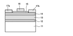
14、104;キャリア供給層、15、105;ショットキ層、
16、106;ゲート電極、17a、107a;ソース電極、
17b、107b:ドレイン電極
Claims (4)
- 基板上に積層したガリウム、アルミニウム、ホウ素及びインジウムからなる群のうち少なくとも1つからなるIII族元素と、窒素、リン及び砒素からなる群のうちの少なくとも窒素を含むV族元素で構成されたIII−V族窒化物半導体層からなる第1の窒化物半導体層と、該第1の窒化物半導体層の上に積層した前記III−V族窒化物半導体層からなり、アルミニウムを含まない第2の窒化物半導体層と、該第2の窒化物半導体層にショットキ接触する制御電極とを備え、前記第2の窒化物半導体層は、微結晶構造からなる窒化物半導体装置において、前記制御電極に印加する制御電圧が0Vのとき、前記制御電極直下の前記第1の窒化物半導体層からなるチャネルにキャリアが存在せず、前記制御電極直下以外の前記チャネルにキャリアが存在していることを特徴とする窒化物半導体装置。
- 請求項1に記載の窒化物半導体装置において、
前記基板と前記第1の窒化物半導体層との間に、前記第1の窒化物半導体層のエネルギーギャップより小さいエネルギーギャップを持つ、前記III−V族窒化物半導体層からなる第3の窒化物半導体層を備え、前記制御電極に印加する制御電圧が0Vのとき、前記制御電極直下の前記第3の窒化物半導体層と前記第1の窒化物半導体層との間に形成されるチャネルにキャリアが存在せず、前記制御電極直下以外の前記チャネルにキャリアが存在していることを特徴とする窒化物半導体装置。 - 請求項1又は2いずれかに記載の窒化物半導体装置において、
前記第2の窒化物半導体層にショットキ接触する前記制御電極と、前記第1の窒化物半導体層にオーミック接触するソース電極及びドレイン電極とを備え、前記第1の窒化物半導体層からなるチャネル、あるいは前記第3の窒化物半導体層と前記第1の窒化物半導体層との間に形成されるチャネルを流れる電流を前記制御電極に印加する電圧により制御することを特徴とする窒化物半導体装置。 - 請求項1乃至3いずれかに記載の窒化物半導体装置において、
前記第2の窒化物半導体層上にオーミック接触する電極を備え、該電極は、成膜状態の前記第2の窒化物半導体層に接触していることを特徴とする窒化物半導体装置。
Priority Applications (1)
| Application Number | Priority Date | Filing Date | Title |
|---|---|---|---|
| JP2005039387A JP4850423B2 (ja) | 2005-02-16 | 2005-02-16 | 窒化物半導体装置 |
Applications Claiming Priority (1)
| Application Number | Priority Date | Filing Date | Title |
|---|---|---|---|
| JP2005039387A JP4850423B2 (ja) | 2005-02-16 | 2005-02-16 | 窒化物半導体装置 |
Publications (2)
| Publication Number | Publication Date |
|---|---|
| JP2006228891A JP2006228891A (ja) | 2006-08-31 |
| JP4850423B2 true JP4850423B2 (ja) | 2012-01-11 |
Family
ID=36990004
Family Applications (1)
| Application Number | Title | Priority Date | Filing Date |
|---|---|---|---|
| JP2005039387A Expired - Fee Related JP4850423B2 (ja) | 2005-02-16 | 2005-02-16 | 窒化物半導体装置 |
Country Status (1)
| Country | Link |
|---|---|
| JP (1) | JP4850423B2 (ja) |
Families Citing this family (5)
| Publication number | Priority date | Publication date | Assignee | Title |
|---|---|---|---|---|
| JP5208439B2 (ja) * | 2007-04-03 | 2013-06-12 | 新日本無線株式会社 | 窒化物半導体装置 |
| JP5285252B2 (ja) * | 2007-09-12 | 2013-09-11 | 新日本無線株式会社 | 窒化物半導体装置 |
| CN102292801B (zh) * | 2009-01-22 | 2013-11-06 | 松下电器产业株式会社 | 场效应晶体管及其制造方法 |
| US8802516B2 (en) | 2010-01-27 | 2014-08-12 | National Semiconductor Corporation | Normally-off gallium nitride-based semiconductor devices |
| JP2011142358A (ja) * | 2011-04-22 | 2011-07-21 | Panasonic Corp | 窒化物半導体装置 |
Family Cites Families (4)
| Publication number | Priority date | Publication date | Assignee | Title |
|---|---|---|---|---|
| JP4022708B2 (ja) * | 2000-06-29 | 2007-12-19 | 日本電気株式会社 | 半導体装置 |
| JP3690594B2 (ja) * | 2001-07-25 | 2005-08-31 | 日本電信電話株式会社 | ナイトライド系化合物半導体の電界効果トランジスタ |
| JP3785970B2 (ja) * | 2001-09-03 | 2006-06-14 | 日本電気株式会社 | Iii族窒化物半導体素子の製造方法 |
| JP3968566B2 (ja) * | 2002-03-26 | 2007-08-29 | 日立電線株式会社 | 窒化物半導体結晶の製造方法及び窒化物半導体ウエハ並びに窒化物半導体デバイス |
-
2005
- 2005-02-16 JP JP2005039387A patent/JP4850423B2/ja not_active Expired - Fee Related
Also Published As
| Publication number | Publication date |
|---|---|
| JP2006228891A (ja) | 2006-08-31 |
Similar Documents
| Publication | Publication Date | Title |
|---|---|---|
| US10707324B2 (en) | Group IIIA-N HEMT with a tunnel diode in the gate stack | |
| US9837519B2 (en) | Semiconductor device | |
| US9196614B2 (en) | Inverted III-nitride P-channel field effect transistor with hole carriers in the channel | |
| TWI431770B (zh) | 半導體裝置及製造其之方法 | |
| JP5334149B2 (ja) | 窒化物半導体電界効果トランジスタ | |
| US8860089B2 (en) | High electron mobility transistor and method of manufacturing the same | |
| US20130240951A1 (en) | Gallium nitride superjunction devices | |
| WO2010109566A1 (ja) | 半導体装置及びその製造方法 | |
| JP2008091392A (ja) | 窒化物半導体装置及びその製造方法 | |
| TW202025493A (zh) | 增強模式化合物半導體場效電晶體、半導體裝置、以及製造增強模式半導體裝置之方法 | |
| WO2011043110A1 (ja) | 半導体装置およびその製造方法 | |
| JP2011029247A (ja) | 窒化物半導体装置及びその製造方法 | |
| JP4869564B2 (ja) | 窒化物半導体装置及びその製造方法 | |
| JP5087240B2 (ja) | 窒化物半導体装置の製造方法 | |
| JP2008078526A (ja) | 窒化物半導体装置及びその製造方法 | |
| KR101172857B1 (ko) | 인헨스먼트 노멀리 오프 질화물 반도체 소자 및 그 제조방법 | |
| JP5100002B2 (ja) | 窒化物半導体装置 | |
| JP4850423B2 (ja) | 窒化物半導体装置 | |
| JP5415668B2 (ja) | 半導体素子 | |
| JP2009289827A (ja) | へテロ接合を有する半導体装置とその製造方法 | |
| JP5208439B2 (ja) | 窒化物半導体装置 | |
| JP5285252B2 (ja) | 窒化物半導体装置 | |
| KR20150044325A (ko) | 고전자 이동도 트랜지스터를 포함하는 전자 장치 | |
| JP2008147552A (ja) | 窒化物半導体装置 |
Legal Events
| Date | Code | Title | Description |
|---|---|---|---|
| A621 | Written request for application examination |
Free format text: JAPANESE INTERMEDIATE CODE: A621 Effective date: 20071022 |
|
| A977 | Report on retrieval |
Free format text: JAPANESE INTERMEDIATE CODE: A971007 Effective date: 20110517 |
|
| A131 | Notification of reasons for refusal |
Free format text: JAPANESE INTERMEDIATE CODE: A131 Effective date: 20110524 |
|
| A521 | Request for written amendment filed |
Free format text: JAPANESE INTERMEDIATE CODE: A523 Effective date: 20110613 |
|
| TRDD | Decision of grant or rejection written | ||
| A01 | Written decision to grant a patent or to grant a registration (utility model) |
Free format text: JAPANESE INTERMEDIATE CODE: A01 Effective date: 20110927 |
|
| A01 | Written decision to grant a patent or to grant a registration (utility model) |
Free format text: JAPANESE INTERMEDIATE CODE: A01 |
|
| A61 | First payment of annual fees (during grant procedure) |
Free format text: JAPANESE INTERMEDIATE CODE: A61 Effective date: 20111019 |
|
| R150 | Certificate of patent or registration of utility model |
Ref document number: 4850423 Country of ref document: JP Free format text: JAPANESE INTERMEDIATE CODE: R150 |
|
| FPAY | Renewal fee payment (event date is renewal date of database) |
Free format text: PAYMENT UNTIL: 20141028 Year of fee payment: 3 |
|
| R250 | Receipt of annual fees |
Free format text: JAPANESE INTERMEDIATE CODE: R250 |
|
| R250 | Receipt of annual fees |
Free format text: JAPANESE INTERMEDIATE CODE: R250 |
|
| R250 | Receipt of annual fees |
Free format text: JAPANESE INTERMEDIATE CODE: R250 |
|
| R250 | Receipt of annual fees |
Free format text: JAPANESE INTERMEDIATE CODE: R250 |
|
| LAPS | Cancellation because of no payment of annual fees |