JP4876237B2 - Linear evaporation source for organic light-emitting device thin film fabrication using multiple crucibles - Google Patents
Linear evaporation source for organic light-emitting device thin film fabrication using multiple crucibles Download PDFInfo
- Publication number
- JP4876237B2 JP4876237B2 JP2007111466A JP2007111466A JP4876237B2 JP 4876237 B2 JP4876237 B2 JP 4876237B2 JP 2007111466 A JP2007111466 A JP 2007111466A JP 2007111466 A JP2007111466 A JP 2007111466A JP 4876237 B2 JP4876237 B2 JP 4876237B2
- Authority
- JP
- Japan
- Prior art keywords
- crucible
- housing
- thin film
- evaporation source
- organic light
- Prior art date
- Legal status (The legal status is an assumption and is not a legal conclusion. Google has not performed a legal analysis and makes no representation as to the accuracy of the status listed.)
- Active
Links
Images




Classifications
-
- C—CHEMISTRY; METALLURGY
- C23—COATING METALLIC MATERIAL; COATING MATERIAL WITH METALLIC MATERIAL; CHEMICAL SURFACE TREATMENT; DIFFUSION TREATMENT OF METALLIC MATERIAL; COATING BY VACUUM EVAPORATION, BY SPUTTERING, BY ION IMPLANTATION OR BY CHEMICAL VAPOUR DEPOSITION, IN GENERAL; INHIBITING CORROSION OF METALLIC MATERIAL OR INCRUSTATION IN GENERAL
- C23C—COATING METALLIC MATERIAL; COATING MATERIAL WITH METALLIC MATERIAL; SURFACE TREATMENT OF METALLIC MATERIAL BY DIFFUSION INTO THE SURFACE, BY CHEMICAL CONVERSION OR SUBSTITUTION; COATING BY VACUUM EVAPORATION, BY SPUTTERING, BY ION IMPLANTATION OR BY CHEMICAL VAPOUR DEPOSITION, IN GENERAL
- C23C14/00—Coating by vacuum evaporation, by sputtering or by ion implantation of the coating forming material
- C23C14/22—Coating by vacuum evaporation, by sputtering or by ion implantation of the coating forming material characterised by the process of coating
- C23C14/24—Vacuum evaporation
- C23C14/243—Crucibles for source material
-
- C—CHEMISTRY; METALLURGY
- C23—COATING METALLIC MATERIAL; COATING MATERIAL WITH METALLIC MATERIAL; CHEMICAL SURFACE TREATMENT; DIFFUSION TREATMENT OF METALLIC MATERIAL; COATING BY VACUUM EVAPORATION, BY SPUTTERING, BY ION IMPLANTATION OR BY CHEMICAL VAPOUR DEPOSITION, IN GENERAL; INHIBITING CORROSION OF METALLIC MATERIAL OR INCRUSTATION IN GENERAL
- C23C—COATING METALLIC MATERIAL; COATING MATERIAL WITH METALLIC MATERIAL; SURFACE TREATMENT OF METALLIC MATERIAL BY DIFFUSION INTO THE SURFACE, BY CHEMICAL CONVERSION OR SUBSTITUTION; COATING BY VACUUM EVAPORATION, BY SPUTTERING, BY ION IMPLANTATION OR BY CHEMICAL VAPOUR DEPOSITION, IN GENERAL
- C23C14/00—Coating by vacuum evaporation, by sputtering or by ion implantation of the coating forming material
- C23C14/06—Coating by vacuum evaporation, by sputtering or by ion implantation of the coating forming material characterised by the coating material
- C23C14/12—Organic material
Landscapes
- Chemical & Material Sciences (AREA)
- Chemical Kinetics & Catalysis (AREA)
- Engineering & Computer Science (AREA)
- Materials Engineering (AREA)
- Mechanical Engineering (AREA)
- Metallurgy (AREA)
- Organic Chemistry (AREA)
- Electroluminescent Light Sources (AREA)
- Physical Vapour Deposition (AREA)
Description
本発明は、複数のルツボを利用した有機発光素子薄膜製作のための線形蒸発源に係り、より詳細には、複数のルツボで蒸発した有機物質が大面積基板に対して均一な蒸着を行わせる有機発光素子薄膜製作のための線形蒸発源に関する。 The present invention relates to a linear evaporation source for manufacturing an organic light emitting device thin film using a plurality of crucibles, and more specifically, allows an organic material evaporated by a plurality of crucibles to be uniformly deposited on a large area substrate. The present invention relates to a linear evaporation source for fabricating an organic light emitting device thin film.
一般的に、有機発光素子を製造する方法は、低分子物質を真空中に蒸発させて製造する方法と、高分子物質を溶剤に溶かしてスピンコーティングする方法とが知られている。 Generally, as a method of manufacturing an organic light emitting device, a method of manufacturing a low molecular weight material by evaporating in a vacuum and a method of spin coating by dissolving a high molecular weight material in a solvent are known.
このような方法のうち、高真空で薄膜を製作する低分子有機発光素子製造方法の場合、任意の形状の開口部を持つシャドーマスクを基板の前に整列して、この基板に有機物質を蒸着して薄膜を製作する。 Among these methods, in the case of a low molecular organic light emitting device manufacturing method in which a thin film is manufactured in a high vacuum, a shadow mask having an opening of an arbitrary shape is aligned in front of the substrate, and an organic material is deposited on the substrate. To produce a thin film.
このような薄膜製作には有機物質蒸発源が利用される。有機物質蒸発源は、上面が開放されて有機物質を入れるルツボ、加熱により蒸発または昇華された有機物質が通過するように複数の穿孔が形成された蓋部を備えて構成される。生産性向上のために大面積基板を使用する場合、大面積薄膜の均一度が確保されるように線形蒸発源が必要になる。この時、大面積基板100または線形蒸発源が動いて基板の全面積に対して蒸着が行われる。 An organic material evaporation source is used for manufacturing such a thin film. The organic material evaporation source is configured to include a crucible in which an upper surface is opened and an organic material is placed, and a lid portion in which a plurality of perforations are formed so that the organic material evaporated or sublimated by heating passes therethrough. When a large area substrate is used to improve productivity, a linear evaporation source is required to ensure the uniformity of the large area thin film. At this time, the large area substrate 100 or the linear evaporation source moves to perform deposition on the entire area of the substrate.
線形蒸発源の外側部分は中央に比べて蒸発されたガスの重畳する部分が少ないために、薄膜の均一度が基板の中央より外側で顕著に小さくなる。このような現象を防止するためには、蒸発源の長さが基板の長さよりかなり長くならねばならないが、この時は蒸発源の使用効率が落ちる。 Since the outer portion of the linear evaporation source has less portions where the evaporated gas overlaps compared to the center, the uniformity of the thin film becomes significantly smaller outside the center of the substrate. In order to prevent such a phenomenon, the length of the evaporation source must be considerably longer than the length of the substrate, but at this time, the use efficiency of the evaporation source is reduced.
図1は、従来の有機発光素子薄膜製作のための線形蒸発源を示す断面図であり、図2は、図1に図示したルツボ蓋部20の平面図である。従来には、大面積均一度の確保のために、蓋部20の穿孔25の間隔とその面積とを調節して長手方向の終端での均一度を向上させようとした。すなわち、図面に示したように、蓋部20の中心から外側へ行くほど穿孔25の間隔を狭め(d1>d2>d3)、穿孔25の面積を広げて(S1<S2<S3)多量の有機物を外側に通過させた。
FIG. 1 is a cross-sectional view showing a conventional linear evaporation source for manufacturing a thin film of an organic light emitting device, and FIG. 2 is a plan view of a
しかし、このように大面積均一度確保のために、穿孔25の大きさが互いに異なり、その間隔が互いに異なる蓋部20を使用する場合、穿孔25の大きさと間隔は非常に微細に調節されねばならない。特に、穿孔25の大きさは、数百μmから数mmまで非常に多様でその加工が非常にむずかしいという問題点がある。また、非常に微細な穿孔25の場合には、蓋部20の熱源変化により有機物が固まって穿孔25が閉塞されがちな問題点がある。
However, in order to secure a large area uniformity in this way, when using the
本発明は、前記した問題点に鑑みてなされたものであり、本発明は、複数のルツボで蒸発した有機物質がルツボの開口から放射状に広がる高さを異にすることによって、微細な穿孔を加工せずに、大面積基板に対して均一な蒸着を行わせるところに目的がある。 The present invention has been made in view of the above-described problems, and the present invention provides fine drilling by varying the height at which organic substances evaporated in a plurality of crucibles spread radially from the crucible openings. The purpose is to allow uniform deposition on a large area substrate without processing.
本発明の目的は、以上で言及した目的に制限されず、言及されていない他の目的は下の記載から当業者に明確に理解されうる。 The objects of the present invention are not limited to the objects mentioned above, and other objects not mentioned can be clearly understood by those skilled in the art from the following description.
前記目的を達成するために、本発明の実施形態による複数のルツボを利用した有機発光素子薄膜製作のための線形蒸発源は、長い筒状ないし箱状に形成されるハウジングと、上面は開放されており、内部に蒸着用物質を入れるものであり、前記ハウジングに挿入される複数のルツボと、前記ルツボを加熱する加熱装置と、を備え、各ルツボの開口の高さが各々異なり、前記ルツボで蒸発された前記蒸着用物質が前記異なる高さのルツボの開口から広がるように構成されている。
In order to achieve the above object, a linear evaporation source for manufacturing an organic light emitting device thin film using a plurality of crucibles according to an embodiment of the present invention includes a housing formed in a long cylindrical shape or a box shape, and an open top surface. A plurality of crucibles inserted into the housing and a heating device for heating the crucibles, each crucible opening having a different height, the crucible The vapor deposition material evaporated in
本発明の有機発光素子薄膜製作のための線形蒸発源によれば、次のような効果が一つあるいはそれ以上ある。 The linear evaporation source for manufacturing the organic light emitting device thin film of the present invention has one or more of the following effects.
第1に、加工し難い微細穿孔をあけなくても有機物質を蒸着させうる。 First, an organic substance can be deposited without drilling fine holes that are difficult to process.
第2に、微細な穿孔が不要なので、有機物が固くなって穿孔が閉塞される問題がない。 Second, since fine perforations are unnecessary, there is no problem that the organic matter becomes hard and the perforations are blocked.
第3に、ハウジング内で各ルツボの有機物質が放射状に広がるルツボの開口の高さを異にして、大面積基板に対して有機物質の均一な蒸着をなしうる。 Third, the organic material can be uniformly deposited on a large-area substrate by changing the height of the crucible opening in which the organic material of each crucible spreads radially in the housing.
その他の実施例の具体的な事項は詳細な説明及び図面に含まれている。 Specific details of other embodiments are included in the detailed description and drawings.
本発明の利点及び特徴、そしてこれを達成する方法は添付された図面に基づいて詳細に後述されている実施例を参照すれば明確になる。しかし、本発明は以下で開示される実施例に限定されるものではなく、この実施例から外れて多様な形に具現でき、本明細書で説明する実施例は本発明の開示を完全にし、本発明が属する技術分野で当業者に発明の範ちゅうを完全に報せるために提供されるものであり、本発明は請求項及び発明の詳細な説明によってのみ定義される。一方、明細書全体に亙って同一な参照符号は同一な構成要素を示す。 Advantages and features of the present invention and methods of achieving the same will be apparent with reference to the embodiments described below in detail with reference to the accompanying drawings. However, the present invention is not limited to the embodiments disclosed below, and can be embodied in various forms that deviate from the embodiments, and the embodiments described herein complete the disclosure of the present invention. The present invention is provided in order to fully inform those skilled in the art in the technical field to which the present invention pertains, and the present invention is defined only by the claims and the detailed description of the invention. On the other hand, the same reference numerals denote the same components throughout the specification.
以下、本発明の実施形態により、複数のルツボを利用した有機発光素子薄膜製作のための線形蒸発源を説明するための図面を参考して本発明について説明する。 Hereinafter, according to an embodiment of the present invention, the present invention will be described with reference to the drawings for describing a linear evaporation source for manufacturing an organic light emitting device thin film using a plurality of crucibles.
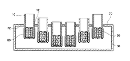
図3は、本発明の第1実施形態による複数のルツボを利用した有機発光素子薄膜製作のための線形蒸発源を示す断面図である。本発明の有機発光素子薄膜製作のための線形蒸発源は、複数のルツボ10を収容するハウジング60、蒸着用物質を入れるルツボ10、ルツボ10を加熱して蒸着用物質を気化または昇華させる加熱装置を備えて構成される。
FIG. 3 is a cross-sectional view illustrating a linear evaporation source for fabricating an organic light emitting device thin film using a plurality of crucibles according to the first embodiment of the present invention. The linear evaporation source for manufacturing the organic light-emitting element thin film of the present invention includes a
ハウジング60は、上面は開放されており、側面と下面とは閉鎖された長い筒状ないし箱状であり、内部に複数のルツボ10を収容するように内部空間を具備する。大面積基板または線形蒸発源が動いて基板の全面積に対して有機物質疑蒸着が行われるように、ハウジング60の幅は基板幅よりはもう少し大きいことが望ましい。
The
ルツボ10は、上面は開放されており、側面と下面とは閉鎖された長い円筒状であり、ルツボ10の内部に蒸着用有機物質50が保存または維持されるように内部空間を具備する。ルツボ10の上端は、そこから蒸発された蒸着用有機物質が広がる開口となっている。ハウジング60には、ルツボ10の上端の開口がハウジング60の上面よりも上方に突出するように、ルツボ10が受け入れられている。図示の例では、各ルツボ10は同じ断面寸法を有しており、したがって、ルツボ10の開口の面積は同じである。
The
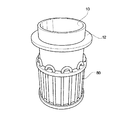
図4は、本発明の一実施形態による熱線80が連結されたルツボ10を示す斜視図である。図4を参照して説明すれば、ルツボ10の形状は長い円筒状であることが望ましい。しかし、上面が開放されており、内部に有機物質50が保存または維持されうるならば、長い四角柱などの形状に多様に変わりうる。ルツボ10の外壁には、後述するルツボ固定部70の係止支持台72に置かれてルツボ10を固定させる係止部12が形成されている。ルツボ10の外壁での係止部12の位置は、ルツボ10がハウジング60に挿入される深さによってルツボ10ごとに異なるが、後述する加熱装置が置かれる位置よりはルツボ10の上部にある必要がある。ルツボ10の外部下端部には加熱装置が形成される。
FIG. 4 is a perspective view showing the
図3を参照すれば、ルツボ10はその高さ寸法がいずれも同じである。そして、ハウジング60内でハウジングの長手方向に沿って一列に配置され、深さを異にして挿入される。ルツボ10の外壁に形成された係止部12の位置をそれぞれ異なって形成できるので、係止支持台72上に係止部12が置かれて、各ルツボ10は深さを異にして挿入されうる。この時、ルツボ10は、中央部から外側(ハウジングの長手方向端部)へ行くほどハウジング60に挿入される深さを浅くする。したがって、中央部から外側へ行くほど蒸発された有機物質50がルツボ10の開口から放射状に広がる高さ(すなわち、ルツボ10の上端の開口の高さ)が高くなる。
Referring to FIG. 3, the
加熱装置は、ルツボ10の外壁に設置されてルツボ10を加熱する。ルツボ10の加熱によりルツボ10の内部に置かれた有機物質50は、温度が上昇して蒸発する。加熱装置は、図4のように熱線80で形成されることが望ましい。熱線80が形成される高さ部位は、ルツボ10の全体高さではなく、ルツボ10の内部に置かれる有機物質50の高さに合わせて形成することが望ましい。各ルツボ10には同量の有機物質50を入れるので、各ルツボ10ごとに熱線80が形成される高さと間隔とを同じくして、各ルツボ10ごとに均一な熱伝逹をなすことが望ましい。したがって、各ルツボ10ごとに蒸発される有機物質50の量は同一になる。加熱装置は、熱線80だけでなくルツボ10の一定高さを加熱できるならば多様な方法で具現できる。
The heating device is installed on the outer wall of the
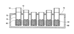
図5は、本発明の第2実施形態による複数のルツボ10を利用した有機発光素子薄膜製作のための線形蒸発源を示す断面図である。複数のルツボ10を収容するハウジング60、蒸着用物質を入れるルツボ10、ルツボ10を加熱して蒸着用物質を気化または昇華させる加熱装置を備えて構成されるが、このような構成要素は前述した第1実施形態と同一であるので、説明を省略する。
FIG. 5 is a cross-sectional view illustrating a linear evaporation source for fabricating an organic light emitting device thin film using a plurality of
ただし、図5を参照すれば、ルツボ10はその高さ寸法が異なる。そして、ハウジング60内でハウジングの長手方向に沿って一列に配置され、挿入される深さはいずれも同じである。この時、ハウジング60の中央から外側へ行くほど高くなるルツボ10を挿入させる。したがって、中央部から外側へ行くほど蒸発された有機物質50がルツボ10の開口から放射状に広がる高さ(すなわち、ルツボ10の上端の開口の高さ)が高くなる。
However, referring to FIG. 5, the height of the
図6は、本発明の第3実施形態による複数のルツボ10を利用した有機発光素子薄膜製作のための線形蒸発源を示す断面図である。複数のルツボ10を収容するハウジング60、蒸着用物質を入れるルツボ10、ルツボ10を加熱して蒸着用物質を気化または昇華させる加熱装置を備えて構成されるが、このような構成要素は前述した第1実施形態と同一であるので、説明を省略する。
FIG. 6 is a cross-sectional view illustrating a linear evaporation source for fabricating an organic light emitting device thin film using a plurality of
ただし、図6を参照すれば、ルツボ10はその高さ寸法がいずれも同じである。そして、ハウジング60内でハウジングの長手方向に沿って一列に配置され、挿入される深さがいずれも同じである。この時、ハウジング60の中央部から外側へ行くほど高さ寸法が大きくなる高さ調節部14がルツボ10上にそれぞれ結合される。高さ調節部14の上端の開口がルツボの開口となっている。したがって、中央部から外側へ行くほど蒸発された有機物質50がルツボ10の開口から放射状に広がる高さ(すなわち、ルツボ10の高さ調節部14の上端の開口の高さ)が高くなる。
However, referring to FIG. 6, the
図7は、蒸発源からの距離による蒸発状態を示す図面である。図面を参照して、本発明によって大面積基板100に対して均一な蒸着が行われる原理を説明する。図7は、有機物質50が蒸発される地点から基板までの距離が近い場合(図7の左側)と、相対的に距離の遠い場合(図7の右側)とを示す。ルツボ10内の一定位置で蒸発された有機物質50は、基板に向う垂直方向を中心に放射状に広がる。放射状に広がるために、有機物質50が蒸発される地点から基板までの距離が近い場合は、遠い場合より狭い地域に有機物質50が到達する。同量の物質が蒸発してさらに狭い地域に有機物質50が到達するので、単位面積当たり有機物質50の量は、距離が近い場合にさらに多くなる。
FIG. 7 is a diagram illustrating an evaporation state depending on a distance from the evaporation source. With reference to the drawings, the principle of performing uniform deposition on the large area substrate 100 according to the present invention will be described. FIG. 7 shows a case where the distance from the point where the
有機物質50がルツボ10の開口から放射状に広がる高さ(ルツボ10の開口の高さ)がそれぞれ同じ場合、外側部分は中央に比べて蒸発された有機物質50の重畳する部分が少なくなる。したがって、蒸発された有機物質50が基板100に蒸着する時、薄膜の均一度が基板100の中心より外側で顕著に小さくなる。
When the height of the
本発明によれば、ルツボ10の開口で有機物質が放射状に広がる高さ(ルツボ10の開口の高さ)が、中央のルツボ10から外側のルツボへ行くほど高くなるように形成される。したがって、外側にあるルツボ10で蒸発した有機物質50は、中央にあるルツボ10で蒸発された有機物質50に比べて重畳する部分は少ないが、基板に垂直な地点のルツボ10から到達する単位面積当たり有機物質50の量は多くなる。したがって、全体ルツボ10で蒸発する有機物質50により大面積基板100に均一な蒸着が行われる。
According to the present invention, the height at which the organic substance spreads radially at the opening of the crucible 10 (the opening height of the crucible 10) is formed so as to increase from the
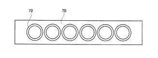
図8は、本発明の一実施形態によるルツボ固定部70の平面図である。ルツボ10の形状によってルツボ10が挿入されるように複数の孔があけられている。ルツボ10に形成された係止部12によりルツボ10が固定されるように、孔には図面のように係止支持台72が形成される。図面に図示していないが、係止部12と係止支持台72とに他の結合手段を付加して、ルツボ10が動かないように固定できる。ルツボ10が挿入される深さを異にして固定する方法は、前記の方法だけでなく多様な方法で具現できる。
FIG. 8 is a plan view of the
前記のように構成される本発明による有機発光素子薄膜製作のための線形蒸発源の作用を説明すれば、次の通りである。 The operation of the linear evaporation source for fabricating the organic light emitting device thin film according to the present invention having the above-described configuration will be described as follows.
ハウジング60上にルツボ固定部70が置かれて結合される。ルツボ固定部70の係止支持台72にルツボ10の係止部12が係止されてルツボ10が固定されるように、各ルツボ10らがハウジング60内に挿入される。この時、それぞれのルツボ10中には同量の有機物が置かれる。ルツボ10に形成された加熱装置は、各ルツボ10において同じ位置に同じ間隔で形成され、各ルツボ10に均一な熱伝逹を行う。したがって、各ルツボ10ごとに同量の有機物質50が蒸発されうる。加熱装置により各ルツボ10で有機物質50が蒸発して、基板に向って上昇する。本発明においては、ハウジング60内の中央から左右方向へ行くほど有機物質50が放射状に広がるルツボ10の開口の高さを高くして、大面積基板に対して均一な有機物質の蒸着が行われる。
A
本発明が属する技術分野で当業者ならば本発明がその技術的思想や必須特徴を変更せずとも他の具体的な形に実施されうるということが理解できるであろう。したがって、前述した実施例は全ての面で例示的なものであって、限定的なものではないと理解せねばならない。本発明の範囲は詳細な説明よりは特許請求の範囲により表れ特許請求の範囲の意味及び範囲、そしてその等価概念から導かれるあらゆる変更または変形された形態が本発明の範囲に含まれると解釈されねばならない。 Those skilled in the art to which the present invention pertains will understand that the present invention may be embodied in other specific forms without altering its technical idea or essential features. Accordingly, it should be understood that the above-described embodiments are illustrative in all aspects and not limiting. The scope of the present invention is defined by the terms of the claims, rather than the detailed description. The meaning and scope of the claims, and any modifications or variations derived from equivalents thereof are construed as being included within the scope of the present invention. I have to.
本発明は、有機発光素子薄膜製作のための線形蒸発源関連の技術分野に好適に用いられる。 The present invention is preferably used in a technical field related to a linear evaporation source for manufacturing an organic light emitting device thin film.
10 ルツボ
12 係止部
50 有機物質
60 ハウジング
70 ルツボ固定部
72 係止支持台
80 熱線
10
Claims (7)
上面は開放されており、内部に蒸着用物質を入れるものであり、前記ハウジングに一列に挿入される複数のルツボと、
前記ルツボを加熱する加熱装置と、を備える有機発光素子薄膜製作のための線形蒸発源において、
各ルツボの開口の高さが各々異なり、前記ルツボで蒸発された前記蒸着用物質が前記異なる高さのルツボの開口から広がるように構成され、前記高さは、前記ハウジングの中央から外側へゆくほど高くなる、有機発光素子薄膜製作のための線形蒸発源。 A long cylindrical or box-shaped housing;
The upper surface is open, the inside of the material for vapor deposition is put, a plurality of crucibles inserted in a row in the housing,
In a linear evaporation source for manufacturing an organic light-emitting element thin film comprising a heating device for heating the crucible,
Each crucible opening has a different opening height, and the deposition material evaporated in the crucible spreads from the crucible opening of the different height, and the height extends from the center of the housing to the outside. more higher, linear evaporation source for the organic light emitting element thin film fabrication.
Applications Claiming Priority (2)
| Application Number | Priority Date | Filing Date | Title |
|---|---|---|---|
| KR10-2006-0046222 | 2006-05-23 | ||
| KR1020060046222A KR100784953B1 (en) | 2006-05-23 | 2006-05-23 | Linear evaporation source for fabrication of organic light emitting device thin film using a large number of crucibles |
Publications (2)
| Publication Number | Publication Date |
|---|---|
| JP2007314873A JP2007314873A (en) | 2007-12-06 |
| JP4876237B2 true JP4876237B2 (en) | 2012-02-15 |
Family
ID=38748342
Family Applications (1)
| Application Number | Title | Priority Date | Filing Date |
|---|---|---|---|
| JP2007111466A Active JP4876237B2 (en) | 2006-05-23 | 2007-04-20 | Linear evaporation source for organic light-emitting device thin film fabrication using multiple crucibles |
Country Status (5)
| Country | Link |
|---|---|
| US (1) | US20070272156A1 (en) |
| JP (1) | JP4876237B2 (en) |
| KR (1) | KR100784953B1 (en) |
| CN (1) | CN101078104A (en) |
| TW (1) | TWI364125B (en) |
Families Citing this family (31)
| Publication number | Priority date | Publication date | Assignee | Title |
|---|---|---|---|---|
| DE102007035166B4 (en) * | 2007-07-27 | 2010-07-29 | Createc Fischer & Co. Gmbh | High-temperature evaporator cell with heating zones connected in parallel, process for their operation and their use in coating plants |
| US7968353B2 (en) | 2008-04-15 | 2011-06-28 | Global Solar Energy, Inc. | Apparatus and methods for manufacturing thin-film solar cells |
| WO2009134041A2 (en) * | 2008-04-29 | 2009-11-05 | Sunic System. Ltd. | Evaporator and vacuum deposition apparatus having the same |
| US20100159132A1 (en) * | 2008-12-18 | 2010-06-24 | Veeco Instruments, Inc. | Linear Deposition Source |
| US20100247809A1 (en) * | 2009-03-31 | 2010-09-30 | Neal James W | Electron beam vapor deposition apparatus for depositing multi-layer coating |
| JP5400653B2 (en) * | 2010-02-16 | 2014-01-29 | 株式会社日立ハイテクノロジーズ | Vacuum deposition equipment |
| JP2011176148A (en) * | 2010-02-24 | 2011-09-08 | Nitto Denko Corp | Method of manufacturing solar cell module, and solar cell module obtained by using the same method |
| CN102212784A (en) * | 2010-04-12 | 2011-10-12 | 无锡尚德太阳能电力有限公司 | Deposition evaporation source |
| KR101730498B1 (en) * | 2010-10-22 | 2017-04-27 | 삼성디스플레이 주식회사 | Apparatus for organic layer deposition, method for manufacturing of organic light emitting display apparatus using the same |
| EP2447393A1 (en) * | 2010-10-27 | 2012-05-02 | Applied Materials, Inc. | Evaporation system and method |
| JP5715802B2 (en) * | 2010-11-19 | 2015-05-13 | 株式会社半導体エネルギー研究所 | Deposition equipment |
| JP6049355B2 (en) * | 2012-08-29 | 2016-12-21 | キヤノントッキ株式会社 | Evaporation source |
| CN104769151B (en) * | 2012-11-14 | 2017-02-22 | 株式会社神户制钢所 | Film forming device |
| CN103898450B (en) * | 2012-12-25 | 2017-06-13 | 北京创昱科技有限公司 | A kind of CIGS co-evaporates linear source device and its application method |
| KR102227546B1 (en) * | 2014-01-20 | 2021-03-15 | 주식회사 선익시스템 | Large capacity evaporation source and Deposition apparatus including the same |
| CN105102087A (en) * | 2014-03-01 | 2015-11-25 | Hzo股份有限公司 | Boats configured to optimize vaporization of precursor materials by material deposition apparatuses |
| CN104178734B (en) * | 2014-07-21 | 2016-06-15 | 京东方科技集团股份有限公司 | Evaporation coating device |
| JP6291696B2 (en) * | 2014-07-28 | 2018-03-14 | 株式会社Joled | Vapor deposition apparatus and evaporation source |
| KR101932943B1 (en) * | 2014-12-05 | 2018-12-27 | 어플라이드 머티어리얼스, 인코포레이티드 | Material deposition system and method for depositing material in a material deposition system |
| KR101649689B1 (en) * | 2015-04-14 | 2016-08-19 | 한국표준과학연구원 | Inductive Heating Linear Evaporation Deposition Apparatus |
| CN105112855A (en) * | 2015-09-29 | 2015-12-02 | 京东方科技集团股份有限公司 | Evaporation crucible and evaporation system |
| JP2017157782A (en) * | 2016-03-04 | 2017-09-07 | ソニー株式会社 | Organic electroluminescent device and method for manufacturing organic electroluminescent device |
| CN105624611B (en) * | 2016-03-29 | 2018-04-24 | 苏州方昇光电股份有限公司 | A kind of rotary organic material vaporising device |
| CN107058957A (en) * | 2017-04-18 | 2017-08-18 | 武汉华星光电技术有限公司 | A kind of evaporation source |
| US11396694B2 (en) | 2017-07-18 | 2022-07-26 | Boe Technology Group Co., Ltd. | Evaporation crucible and evaporation apparatus |
| US20210062323A1 (en) * | 2017-09-14 | 2021-03-04 | Alpha Plus Co., Ltd. | Vacuum evaporation source |
| CN110055498B (en) * | 2018-01-19 | 2022-08-12 | 京东方科技集团股份有限公司 | Surface vapor deposition source and its production method, vapor deposition method, and vapor deposition device |
| KR102921715B1 (en) * | 2020-06-29 | 2026-02-04 | 삼성디스플레이 주식회사 | Crucible and method of depositing deposition material using crucible |
| DE102020133979A1 (en) | 2020-12-17 | 2022-06-23 | Phoenix Silicon International Corp. | CRUCIBLE AND VAPOR DEVICE |
| US12454750B2 (en) | 2021-08-12 | 2025-10-28 | Elevated Materials Us Llc | Evaporator for effective surface area evaporation |
| CN114836721B (en) * | 2022-04-25 | 2024-01-26 | 山东国晶新材料有限公司 | Ceramic point source for horizontal transverse arrangement |
Family Cites Families (16)
| Publication number | Priority date | Publication date | Assignee | Title |
|---|---|---|---|---|
| DE3904607A1 (en) * | 1989-02-16 | 1990-08-23 | Leybold Ag | DIRECTLY HEATABLE MELT CONTAINER FOR INDUCTION MELTING OVENS |
| US5525156A (en) * | 1989-11-24 | 1996-06-11 | Research Development Corporation | Apparatus for epitaxially growing a chemical compound crystal |
| JP3371454B2 (en) * | 1993-01-13 | 2003-01-27 | 石川島播磨重工業株式会社 | Continuous vacuum deposition equipment |
| US5803976A (en) * | 1993-11-09 | 1998-09-08 | Imperial Chemical Industries Plc | Vacuum web coating |
| US5616180A (en) * | 1994-12-22 | 1997-04-01 | Northrop Grumman Corporation | Aparatus for varying the flux of a molecular beam |
| AU747717B2 (en) * | 1997-11-12 | 2002-05-23 | Ppa Water Industries (Proprietary) Limited | Means for chemical water treatment |
| US6068441A (en) * | 1997-11-21 | 2000-05-30 | Asm America, Inc. | Substrate transfer system for semiconductor processing equipment |
| US6310281B1 (en) * | 2000-03-16 | 2001-10-30 | Global Solar Energy, Inc. | Thin-film, flexible photovoltaic module |
| US20040035360A1 (en) * | 2002-05-17 | 2004-02-26 | Semiconductor Energy Laboratory Co., Ltd. | Manufacturing apparatus |
| US20030221620A1 (en) * | 2002-06-03 | 2003-12-04 | Semiconductor Energy Laboratory Co., Ltd. | Vapor deposition device |
| TWI277363B (en) * | 2002-08-30 | 2007-03-21 | Semiconductor Energy Lab | Fabrication system, light-emitting device and fabricating method of organic compound-containing layer |
| KR100532657B1 (en) * | 2002-11-18 | 2005-12-02 | 주식회사 야스 | Apparatus for controlling deposition zone of homogeneously mixed layer in multi source co-deposition |
| US20080282983A1 (en) * | 2003-12-09 | 2008-11-20 | Braddock Iv Walter David | High Temperature Vacuum Evaporation Apparatus |
| KR20060030426A (en) * | 2004-10-05 | 2006-04-10 | 삼성에스디아이 주식회사 | Vacuum deposition apparatus and vacuum deposition method |
| JP4552184B2 (en) * | 2004-10-22 | 2010-09-29 | 富士電機ホールディングス株式会社 | Apparatus and method for depositing organic layer on substrate for organic light emitting device |
| KR100592304B1 (en) * | 2004-11-05 | 2006-06-21 | 삼성에스디아이 주식회사 | Heating vessel and deposition apparatus having the same |
-
2006
- 2006-05-23 KR KR1020060046222A patent/KR100784953B1/en active Active
-
2007
- 2007-04-20 JP JP2007111466A patent/JP4876237B2/en active Active
- 2007-05-14 US US11/803,297 patent/US20070272156A1/en not_active Abandoned
- 2007-05-16 CN CN200710103720.0A patent/CN101078104A/en active Pending
- 2007-05-17 TW TW096117672A patent/TWI364125B/en active
Also Published As
| Publication number | Publication date |
|---|---|
| KR100784953B1 (en) | 2007-12-11 |
| KR20070113410A (en) | 2007-11-29 |
| TWI364125B (en) | 2012-05-11 |
| CN101078104A (en) | 2007-11-28 |
| US20070272156A1 (en) | 2007-11-29 |
| TW200744242A (en) | 2007-12-01 |
| JP2007314873A (en) | 2007-12-06 |
Similar Documents
| Publication | Publication Date | Title |
|---|---|---|
| JP4876237B2 (en) | Linear evaporation source for organic light-emitting device thin film fabrication using multiple crucibles | |
| KR101094299B1 (en) | Linear evaporation source and deposition apparatus comprising the same | |
| JP2011132596A (en) | Evaporation source and vapor-deposition apparatus using the same | |
| JP4847365B2 (en) | Vapor deposition source and vapor deposition apparatus | |
| KR20070112668A (en) | Linear Evaporator for Fabrication of Organic Thin Film | |
| US20100043710A1 (en) | Inner plate and crucible assembly for deposition having the same | |
| KR100805531B1 (en) | Evaporation source | |
| KR100862340B1 (en) | Linear Evaporation Source for Fabrication of Organic Light-Emitting Thin Film | |
| KR100473485B1 (en) | Linear type evaporator for manufacturing elements of organic semiconductor device | |
| JP2005520933A (en) | Evaporation source for vapor deposition process, insulating fixing plate applied thereto, hot wire winding plate, and hot wire fixing method | |
| KR100434438B1 (en) | Circular nozzle source for thermal evaporation process | |
| KR100758694B1 (en) | Linear Evaporator for Fabrication of Organic Thin Film | |
| KR102138990B1 (en) | A system comprising a crucible for melting and heating the material and a crucible and heater configuration | |
| KR101131599B1 (en) | Evaporator and vacuum evaporation apparatus having the same | |
| KR20150069833A (en) | Evaporation apparatus | |
| JP4478113B2 (en) | Heating vessel support and vapor deposition apparatus equipped with the same | |
| JP2008024998A (en) | Vacuum deposition source and vacuum deposition equipment | |
| KR100829736B1 (en) | Heating vessel of vacuum deposition equipment | |
| JP2007224393A (en) | Vapor deposition source cell, thin film deposition method, aperture diaphragm member, and vapor deposition source heater | |
| KR20100108086A (en) | Linear type evaporator and vacuum evaporation apparatus having the same | |
| KR100994454B1 (en) | Evaporation apparatus and vacuum deposition apparatus having the same | |
| KR20080000432A (en) | Shadow mask, deposition apparatus including the same, and manufacturing method of organic light emitting device using the deposition apparatus | |
| KR20070051602A (en) | Organic Vacuum Deposition Device | |
| KR102114864B1 (en) | Downward OLED Deposition Apparatus | |
| KR102733478B1 (en) | Lateral type vacuum effusion cell and method for fabricating organic light emitting display device using the same |
Legal Events
| Date | Code | Title | Description |
|---|---|---|---|
| A977 | Report on retrieval |
Free format text: JAPANESE INTERMEDIATE CODE: A971007 Effective date: 20100428 |
|
| A131 | Notification of reasons for refusal |
Free format text: JAPANESE INTERMEDIATE CODE: A131 Effective date: 20100506 |
|
| A521 | Request for written amendment filed |
Free format text: JAPANESE INTERMEDIATE CODE: A523 Effective date: 20100729 |
|
| A131 | Notification of reasons for refusal |
Free format text: JAPANESE INTERMEDIATE CODE: A131 Effective date: 20101130 |
|
| TRDD | Decision of grant or rejection written | ||
| A01 | Written decision to grant a patent or to grant a registration (utility model) |
Free format text: JAPANESE INTERMEDIATE CODE: A01 Effective date: 20111025 |
|
| A01 | Written decision to grant a patent or to grant a registration (utility model) |
Free format text: JAPANESE INTERMEDIATE CODE: A01 |
|
| A61 | First payment of annual fees (during grant procedure) |
Free format text: JAPANESE INTERMEDIATE CODE: A61 Effective date: 20111102 |
|
| R150 | Certificate of patent or registration of utility model |
Free format text: JAPANESE INTERMEDIATE CODE: R150 Ref document number: 4876237 Country of ref document: JP Free format text: JAPANESE INTERMEDIATE CODE: R150 |
|
| FPAY | Renewal fee payment (event date is renewal date of database) |
Free format text: PAYMENT UNTIL: 20141209 Year of fee payment: 3 |
|
| R250 | Receipt of annual fees |
Free format text: JAPANESE INTERMEDIATE CODE: R250 |
|
| R250 | Receipt of annual fees |
Free format text: JAPANESE INTERMEDIATE CODE: R250 |
|
| R250 | Receipt of annual fees |
Free format text: JAPANESE INTERMEDIATE CODE: R250 |
|
| R250 | Receipt of annual fees |
Free format text: JAPANESE INTERMEDIATE CODE: R250 |
|
| R250 | Receipt of annual fees |
Free format text: JAPANESE INTERMEDIATE CODE: R250 |
|
| R250 | Receipt of annual fees |
Free format text: JAPANESE INTERMEDIATE CODE: R250 |
|
| R250 | Receipt of annual fees |
Free format text: JAPANESE INTERMEDIATE CODE: R250 |
|
| R250 | Receipt of annual fees |
Free format text: JAPANESE INTERMEDIATE CODE: R250 |
|
| R250 | Receipt of annual fees |
Free format text: JAPANESE INTERMEDIATE CODE: R250 |
|
| R250 | Receipt of annual fees |
Free format text: JAPANESE INTERMEDIATE CODE: R250 |
|
| R250 | Receipt of annual fees |
Free format text: JAPANESE INTERMEDIATE CODE: R250 |
|
| R250 | Receipt of annual fees |
Free format text: JAPANESE INTERMEDIATE CODE: R250 |