JP4880958B2 - 半導体装置及びその製造方法 - Google Patents
半導体装置及びその製造方法 Download PDFInfo
- Publication number
- JP4880958B2 JP4880958B2 JP2005270773A JP2005270773A JP4880958B2 JP 4880958 B2 JP4880958 B2 JP 4880958B2 JP 2005270773 A JP2005270773 A JP 2005270773A JP 2005270773 A JP2005270773 A JP 2005270773A JP 4880958 B2 JP4880958 B2 JP 4880958B2
- Authority
- JP
- Japan
- Prior art keywords
- stress
- silicide
- forming
- gate electrode
- annealing
- Prior art date
- Legal status (The legal status is an assumption and is not a legal conclusion. Google has not performed a legal analysis and makes no representation as to the accuracy of the status listed.)
- Expired - Fee Related
Links
Images




Classifications
-
- H—ELECTRICITY
- H10—SEMICONDUCTOR DEVICES; ELECTRIC SOLID-STATE DEVICES NOT OTHERWISE PROVIDED FOR
- H10D—INORGANIC ELECTRIC SEMICONDUCTOR DEVICES
- H10D30/00—Field-effect transistors [FET]
- H10D30/01—Manufacture or treatment
- H10D30/021—Manufacture or treatment of FETs having insulated gates [IGFET]
- H10D30/0223—Manufacture or treatment of FETs having insulated gates [IGFET] having source and drain regions or source and drain extensions self-aligned to sides of the gate
- H10D30/0227—Manufacture or treatment of FETs having insulated gates [IGFET] having source and drain regions or source and drain extensions self-aligned to sides of the gate having both lightly-doped source and drain extensions and source and drain regions self-aligned to the sides of the gate, e.g. lightly-doped drain [LDD] MOSFET or double-diffused drain [DDD] MOSFET
-
- H—ELECTRICITY
- H10—SEMICONDUCTOR DEVICES; ELECTRIC SOLID-STATE DEVICES NOT OTHERWISE PROVIDED FOR
- H10D—INORGANIC ELECTRIC SEMICONDUCTOR DEVICES
- H10D30/00—Field-effect transistors [FET]
- H10D30/60—Insulated-gate field-effect transistors [IGFET]
- H10D30/601—Insulated-gate field-effect transistors [IGFET] having lightly-doped drain or source extensions, e.g. LDD IGFETs or DDD IGFETs
-
- H—ELECTRICITY
- H10—SEMICONDUCTOR DEVICES; ELECTRIC SOLID-STATE DEVICES NOT OTHERWISE PROVIDED FOR
- H10D—INORGANIC ELECTRIC SEMICONDUCTOR DEVICES
- H10D30/00—Field-effect transistors [FET]
- H10D30/60—Insulated-gate field-effect transistors [IGFET]
- H10D30/791—Arrangements for exerting mechanical stress on the crystal lattice of the channel regions
- H10D30/794—Arrangements for exerting mechanical stress on the crystal lattice of the channel regions comprising conductive materials, e.g. silicided source, drain or gate electrodes
-
- H—ELECTRICITY
- H10—SEMICONDUCTOR DEVICES; ELECTRIC SOLID-STATE DEVICES NOT OTHERWISE PROVIDED FOR
- H10D—INORGANIC ELECTRIC SEMICONDUCTOR DEVICES
- H10D84/00—Integrated devices formed in or on semiconductor substrates that comprise only semiconducting layers, e.g. on Si wafers or on GaAs-on-Si wafers
- H10D84/01—Manufacture or treatment
- H10D84/0123—Integrating together multiple components covered by H10D12/00 or H10D30/00, e.g. integrating multiple IGBTs
- H10D84/0126—Integrating together multiple components covered by H10D12/00 or H10D30/00, e.g. integrating multiple IGBTs the components including insulated gates, e.g. IGFETs
- H10D84/0165—Integrating together multiple components covered by H10D12/00 or H10D30/00, e.g. integrating multiple IGBTs the components including insulated gates, e.g. IGFETs the components including complementary IGFETs, e.g. CMOS devices
- H10D84/0167—Manufacturing their channels
-
- H—ELECTRICITY
- H10—SEMICONDUCTOR DEVICES; ELECTRIC SOLID-STATE DEVICES NOT OTHERWISE PROVIDED FOR
- H10D—INORGANIC ELECTRIC SEMICONDUCTOR DEVICES
- H10D84/00—Integrated devices formed in or on semiconductor substrates that comprise only semiconducting layers, e.g. on Si wafers or on GaAs-on-Si wafers
- H10D84/01—Manufacture or treatment
- H10D84/0123—Integrating together multiple components covered by H10D12/00 or H10D30/00, e.g. integrating multiple IGBTs
- H10D84/0126—Integrating together multiple components covered by H10D12/00 or H10D30/00, e.g. integrating multiple IGBTs the components including insulated gates, e.g. IGFETs
- H10D84/0165—Integrating together multiple components covered by H10D12/00 or H10D30/00, e.g. integrating multiple IGBTs the components including insulated gates, e.g. IGFETs the components including complementary IGFETs, e.g. CMOS devices
- H10D84/017—Manufacturing their source or drain regions, e.g. silicided source or drain regions
-
- H—ELECTRICITY
- H10—SEMICONDUCTOR DEVICES; ELECTRIC SOLID-STATE DEVICES NOT OTHERWISE PROVIDED FOR
- H10D—INORGANIC ELECTRIC SEMICONDUCTOR DEVICES
- H10D84/00—Integrated devices formed in or on semiconductor substrates that comprise only semiconducting layers, e.g. on Si wafers or on GaAs-on-Si wafers
- H10D84/01—Manufacture or treatment
- H10D84/02—Manufacture or treatment characterised by using material-based technologies
- H10D84/03—Manufacture or treatment characterised by using material-based technologies using Group IV technology, e.g. silicon technology or silicon-carbide [SiC] technology
- H10D84/038—Manufacture or treatment characterised by using material-based technologies using Group IV technology, e.g. silicon technology or silicon-carbide [SiC] technology using silicon technology, e.g. SiGe
Landscapes
- Insulated Gate Type Field-Effect Transistor (AREA)
- Metal-Oxide And Bipolar Metal-Oxide Semiconductor Integrated Circuits (AREA)
- Electrodes Of Semiconductors (AREA)
Description
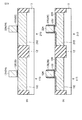
前記第1のゲート電極を挟んで前記半導体基板中に形成された第1の拡散層と、
前記第1の拡散層に形成され、少なくとも1つの金属を含む金属シリサイドから構成された引っ張り応力を内在する第1の導電体層とを具備するnMOSFETと、
前記半導体基板上に絶縁膜を介して形成された第2のゲート電極と、
前記第2のゲート電極を挟んで前記半導体基板中に形成された第2の拡散層と、
前記第2の拡散層に形成され、前記少なくとも1つの金属を含む金属シリサイドから構成され、前記少なくとも1つの金属とシリコンとの組成比が前記第1の導電体層の組成比と同じである、圧縮応力を内在する第2の導電体層とを具備するpMOSFETと、
を具備する。
Claims (5)
- 半導体基板上に絶縁膜を介して形成された第1のゲート電極と、
前記第1のゲート電極を挟んで前記半導体基板中に形成された第1の拡散層と、
前記第1の拡散層に形成され、少なくとも1つの金属を含む金属シリサイドから構成された引っ張り応力を内在する第1の導電体層とを具備するnMOSFETと、
前記半導体基板上に絶縁膜を介して形成された第2のゲート電極と、
前記第2のゲート電極を挟んで前記半導体基板中に形成された第2の拡散層と、
前記第2の拡散層に形成され、前記少なくとも1つの金属を含む金属シリサイドから構成され、前記少なくとも1つの金属とシリコンとの組成比が前記第1の導電体層の組成比と同じである、圧縮応力を内在する第2の導電体層とを具備するpMOSFETと、
を具備することを特徴とする半導体装置。 - 前記少なくとも1つの金属は、ニッケル、コバルト、チタニウム、プラチナ、パラジウムあるいはエルビウムであることを特徴とする、請求項1に記載の半導体装置。
- 前記引っ張り及び圧縮の内部応力は、前記第1及び第2の導電体層を形成する際に同時に形成されることを特徴とする、請求項1または2に記載の半導体装置。
- 半導体基板中にnMOSFET形成用の第1の半導体領域およびpMOSFET形成用の第2の半導体領域を形成する工程と、
前記第1の半導体領域上に絶縁膜を介して第1のゲート電極を形成し、前記第2の半導体領域上に絶縁膜を介して第2のゲート電極を形成する工程と、
前記第1のゲート電極を挟む前記半導体基板中に第1の拡散層を形成し、前記第2のゲート電極を挟む前記半導体基板中に第2の拡散層を形成する工程と、
前記第1及び第2の拡散層に接触させて金属材料を堆積する工程と、
第1のアニールにより前記金属材料と前記半導体基板とを反応させて前記第1及び第2の拡散層上に引っ張り応力を内在する第1相の第1及び第2の導電体層をそれぞれ形成する工程と、
前記第2の半導体領域上に圧縮応力を内在する応力制御膜を形成する工程と、
第2のアニールにより第1の半導体領域に前記引っ張り応力を内在する第2相の第1の導電体層を形成し、第2の半導体領域に前記圧縮応力を内在する第2相の第2の導電体層を形成する工程と、
を具備することを特徴とする、半導体装置の製造方法。 - 前記第1のアニールは、前記第2のアニールより、低温、短時間で行われることを特徴とする請求項4に記載の半導体装置の製造方法。
Priority Applications (3)
| Application Number | Priority Date | Filing Date | Title |
|---|---|---|---|
| JP2005270773A JP4880958B2 (ja) | 2005-09-16 | 2005-09-16 | 半導体装置及びその製造方法 |
| US11/340,517 US7372108B2 (en) | 2005-09-16 | 2006-01-27 | Semiconductor device and manufacturing method thereof |
| US12/081,439 US7741220B2 (en) | 2005-09-16 | 2008-04-16 | Semiconductor device and manufacturing method thereof |
Applications Claiming Priority (1)
| Application Number | Priority Date | Filing Date | Title |
|---|---|---|---|
| JP2005270773A JP4880958B2 (ja) | 2005-09-16 | 2005-09-16 | 半導体装置及びその製造方法 |
Publications (2)
| Publication Number | Publication Date |
|---|---|
| JP2007081330A JP2007081330A (ja) | 2007-03-29 |
| JP4880958B2 true JP4880958B2 (ja) | 2012-02-22 |
Family
ID=37884717
Family Applications (1)
| Application Number | Title | Priority Date | Filing Date |
|---|---|---|---|
| JP2005270773A Expired - Fee Related JP4880958B2 (ja) | 2005-09-16 | 2005-09-16 | 半導体装置及びその製造方法 |
Country Status (2)
| Country | Link |
|---|---|
| US (2) | US7372108B2 (ja) |
| JP (1) | JP4880958B2 (ja) |
Families Citing this family (24)
| Publication number | Priority date | Publication date | Assignee | Title |
|---|---|---|---|---|
| JP4880958B2 (ja) * | 2005-09-16 | 2012-02-22 | 株式会社東芝 | 半導体装置及びその製造方法 |
| US7696019B2 (en) * | 2006-03-09 | 2010-04-13 | Infineon Technologies Ag | Semiconductor devices and methods of manufacturing thereof |
| US20080142897A1 (en) * | 2006-12-19 | 2008-06-19 | Chartered Semiconductor Manufacturing Ltd. | Integrated circuit system having strained transistor |
| US20080217700A1 (en) * | 2007-03-11 | 2008-09-11 | Doris Bruce B | Mobility Enhanced FET Devices |
| US7494937B2 (en) * | 2007-03-30 | 2009-02-24 | Tokyo Electron Limited | Strained metal silicon nitride films and method of forming |
| US7531452B2 (en) * | 2007-03-30 | 2009-05-12 | Tokyo Electron Limited | Strained metal silicon nitride films and method of forming |
| US7713868B2 (en) * | 2007-03-30 | 2010-05-11 | Tokyo Electron Limited | Strained metal nitride films and method of forming |
| US8178446B2 (en) * | 2007-03-30 | 2012-05-15 | Tokyo Electron Limited | Strained metal nitride films and method of forming |
| TW200910526A (en) * | 2007-07-03 | 2009-03-01 | Renesas Tech Corp | Method of manufacturing semiconductor device |
| JP2009260004A (ja) * | 2008-04-16 | 2009-11-05 | Renesas Technology Corp | 半導体装置の製造方法 |
| US7985652B2 (en) * | 2007-09-14 | 2011-07-26 | Taiwan Semiconductor Manufacturing Company, Ltd. | Metal stress memorization technology |
| JP2009158621A (ja) * | 2007-12-25 | 2009-07-16 | Toshiba Corp | 半導体装置 |
| KR101406226B1 (ko) * | 2008-05-07 | 2014-06-13 | 삼성전자주식회사 | 반도체 소자의 제조 방법 |
| JP4770885B2 (ja) * | 2008-06-30 | 2011-09-14 | ソニー株式会社 | 半導体装置 |
| DE102009006800B4 (de) * | 2009-01-30 | 2013-01-31 | Advanced Micro Devices, Inc. | Verfahren zur Herstellung von Transistoren und entsprechendes Halbleiterbauelement |
| JP5569243B2 (ja) | 2010-08-09 | 2014-08-13 | ソニー株式会社 | 半導体装置及びその製造方法 |
| JP4771024B2 (ja) * | 2011-04-15 | 2011-09-14 | ソニー株式会社 | 半導体装置の製造方法 |
| US9093361B2 (en) | 2011-06-23 | 2015-07-28 | Mitsubishi Electric Corporation | Semiconductor device |
| FR2979480B1 (fr) * | 2011-08-25 | 2013-09-27 | Commissariat Energie Atomique | Procede de realisation d'un dispositif a transistors contraints par siliciuration des zones de source et de drain |
| FR2979482B1 (fr) * | 2011-08-25 | 2013-09-27 | Commissariat Energie Atomique | Procede de realisation d'un dispositif a transistors contraints a l'aide d'une couche externe |
| KR101876793B1 (ko) | 2012-02-27 | 2018-07-11 | 삼성전자주식회사 | 전계효과 트랜지스터 및 그 제조 방법 |
| CN103311281B (zh) * | 2012-03-14 | 2016-03-30 | 中国科学院微电子研究所 | 半导体器件及其制造方法 |
| US20140048888A1 (en) * | 2012-08-17 | 2014-02-20 | Taiwan Semiconductor Manufacturing Company, Ltd. | Strained Structure of a Semiconductor Device |
| JP6178065B2 (ja) * | 2012-10-09 | 2017-08-09 | 株式会社東芝 | 半導体装置 |
Family Cites Families (19)
| Publication number | Priority date | Publication date | Assignee | Title |
|---|---|---|---|---|
| JP2003086708A (ja) * | 2000-12-08 | 2003-03-20 | Hitachi Ltd | 半導体装置及びその製造方法 |
| JP2005057301A (ja) | 2000-12-08 | 2005-03-03 | Renesas Technology Corp | 半導体装置及びその製造方法 |
| JP2003060076A (ja) * | 2001-08-21 | 2003-02-28 | Nec Corp | 半導体装置及びその製造方法 |
| JP4173672B2 (ja) * | 2002-03-19 | 2008-10-29 | 株式会社ルネサステクノロジ | 半導体装置及びその製造方法 |
| KR100500451B1 (ko) * | 2003-06-16 | 2005-07-12 | 삼성전자주식회사 | 인장된 채널을 갖는 모스 트랜지스터를 구비하는반도체소자의 제조 방법 |
| JP4860102B2 (ja) * | 2003-06-26 | 2012-01-25 | ルネサスエレクトロニクス株式会社 | 半導体装置 |
| KR101025761B1 (ko) * | 2004-03-30 | 2011-04-04 | 삼성전자주식회사 | 디지탈 회로 및 아날로그 회로를 가지는 반도체 집적회로및 그 제조 방법 |
| US7173312B2 (en) * | 2004-12-15 | 2007-02-06 | International Business Machines Corporation | Structure and method to generate local mechanical gate stress for MOSFET channel mobility modification |
| US20060163670A1 (en) * | 2005-01-27 | 2006-07-27 | International Business Machines Corporation | Dual silicide process to improve device performance |
| US7224033B2 (en) * | 2005-02-15 | 2007-05-29 | International Business Machines Corporation | Structure and method for manufacturing strained FINFET |
| DE102005030583B4 (de) * | 2005-06-30 | 2010-09-30 | Advanced Micro Devices, Inc., Sunnyvale | Verfahren zur Herstellung von Kontaktisolationsschichten und Silizidgebieten mit unterschiedlichen Eigenschaften eines Halbleiterbauelements und Halbleiterbauelement |
| US20070018252A1 (en) * | 2005-07-21 | 2007-01-25 | International Business Machines Corporation | Semiconductor device containing high performance p-mosfet and/or n-mosfet and method of fabricating the same |
| US7470943B2 (en) * | 2005-08-22 | 2008-12-30 | International Business Machines Corporation | High performance MOSFET comprising a stressed gate metal silicide layer and method of fabricating the same |
| JP4880958B2 (ja) * | 2005-09-16 | 2012-02-22 | 株式会社東芝 | 半導体装置及びその製造方法 |
| US7709317B2 (en) * | 2005-11-14 | 2010-05-04 | International Business Machines Corporation | Method to increase strain enhancement with spacerless FET and dual liner process |
| US7504336B2 (en) * | 2006-05-19 | 2009-03-17 | International Business Machines Corporation | Methods for forming CMOS devices with intrinsically stressed metal silicide layers |
| JP2008244059A (ja) * | 2007-03-27 | 2008-10-09 | Renesas Technology Corp | 半導体装置の製造方法 |
| TW200910526A (en) * | 2007-07-03 | 2009-03-01 | Renesas Tech Corp | Method of manufacturing semiconductor device |
| US8349732B2 (en) * | 2008-07-18 | 2013-01-08 | Taiwan Semiconductor Manufacturing Company, Ltd. | Implanted metal silicide for semiconductor device |
-
2005
- 2005-09-16 JP JP2005270773A patent/JP4880958B2/ja not_active Expired - Fee Related
-
2006
- 2006-01-27 US US11/340,517 patent/US7372108B2/en not_active Expired - Fee Related
-
2008
- 2008-04-16 US US12/081,439 patent/US7741220B2/en not_active Expired - Fee Related
Also Published As
| Publication number | Publication date |
|---|---|
| JP2007081330A (ja) | 2007-03-29 |
| US7741220B2 (en) | 2010-06-22 |
| US20090227079A1 (en) | 2009-09-10 |
| US7372108B2 (en) | 2008-05-13 |
| US20070066001A1 (en) | 2007-03-22 |
Similar Documents
| Publication | Publication Date | Title |
|---|---|---|
| JP4880958B2 (ja) | 半導体装置及びその製造方法 | |
| CN101295733B (zh) | 半导体元件 | |
| KR101027107B1 (ko) | 완전 변환된 반도체 금속 합금에 의한 금속 게이트mosfet | |
| US7084061B2 (en) | Methods of fabricating a semiconductor device having MOS transistor with strained channel | |
| JP2751895B2 (ja) | 半導体装置の製造方法 | |
| CN101093805A (zh) | 半导体器件的制造方法以及半导体器件 | |
| JP2009088069A (ja) | 半導体装置及びその製造方法 | |
| JP5117740B2 (ja) | 半導体装置の製造方法 | |
| JP2005217275A (ja) | 半導体装置およびその製造方法 | |
| US20060094196A1 (en) | Method of fabricating semiconductor device, and semiconductor device | |
| WO2007031928A2 (en) | Method of manufacturing semiconductor device with different metallic gates | |
| JP3998665B2 (ja) | 半導体装置およびその製造方法 | |
| JP2008124393A (ja) | 半導体装置の製造方法 | |
| US7994586B2 (en) | Semiconductor device and manufacturing method of the same | |
| US7994591B2 (en) | Semiconductor device and method for manufacturing the same | |
| JP2009076731A (ja) | 半導体装置およびその製造方法 | |
| JP2009043938A (ja) | 半導体装置および半導体装置の製造方法 | |
| JP2009164200A (ja) | 半導体装置及びその製造方法 | |
| JP2009277909A (ja) | 半導体装置の製造方法 | |
| US7348233B1 (en) | Methods for fabricating a CMOS device including silicide contacts | |
| JP2008103644A (ja) | 半導体装置およびその製造方法 | |
| JP2006196646A (ja) | 半導体装置及びその製造方法 | |
| JPWO2009084376A1 (ja) | 半導体装置及びその製造方法 | |
| US7544553B2 (en) | Integration scheme for fully silicided gate | |
| JP2008047586A (ja) | 半導体装置およびその製造方法 |
Legal Events
| Date | Code | Title | Description |
|---|---|---|---|
| A621 | Written request for application examination |
Free format text: JAPANESE INTERMEDIATE CODE: A621 Effective date: 20080718 |
|
| A977 | Report on retrieval |
Free format text: JAPANESE INTERMEDIATE CODE: A971007 Effective date: 20101019 |
|
| A131 | Notification of reasons for refusal |
Free format text: JAPANESE INTERMEDIATE CODE: A131 Effective date: 20110809 |
|
| A521 | Request for written amendment filed |
Free format text: JAPANESE INTERMEDIATE CODE: A523 Effective date: 20111011 |
|
| TRDD | Decision of grant or rejection written | ||
| A01 | Written decision to grant a patent or to grant a registration (utility model) |
Free format text: JAPANESE INTERMEDIATE CODE: A01 Effective date: 20111108 |
|
| A01 | Written decision to grant a patent or to grant a registration (utility model) |
Free format text: JAPANESE INTERMEDIATE CODE: A01 |
|
| A61 | First payment of annual fees (during grant procedure) |
Free format text: JAPANESE INTERMEDIATE CODE: A61 Effective date: 20111202 |
|
| FPAY | Renewal fee payment (event date is renewal date of database) |
Free format text: PAYMENT UNTIL: 20141209 Year of fee payment: 3 |
|
| LAPS | Cancellation because of no payment of annual fees |