JP4884018B2 - 増幅装置、および光ディスクドライブ装置 - Google Patents
増幅装置、および光ディスクドライブ装置 Download PDFInfo
- Publication number
- JP4884018B2 JP4884018B2 JP2006027813A JP2006027813A JP4884018B2 JP 4884018 B2 JP4884018 B2 JP 4884018B2 JP 2006027813 A JP2006027813 A JP 2006027813A JP 2006027813 A JP2006027813 A JP 2006027813A JP 4884018 B2 JP4884018 B2 JP 4884018B2
- Authority
- JP
- Japan
- Prior art keywords
- phase compensation
- unit
- signal
- optical disk
- bipolar transistor
- Prior art date
- Legal status (The legal status is an assumption and is not a legal conclusion. Google has not performed a legal analysis and makes no representation as to the accuracy of the status listed.)
- Expired - Fee Related
Links
Images


Classifications
-
- H—ELECTRICITY
- H03—ELECTRONIC CIRCUITRY
- H03F—AMPLIFIERS
- H03F3/00—Amplifiers with only discharge tubes or only semiconductor devices as amplifying elements
- H03F3/34—DC amplifiers in which all stages are DC-coupled
- H03F3/343—DC amplifiers in which all stages are DC-coupled with semiconductor devices only
- H03F3/3432—DC amplifiers in which all stages are DC-coupled with semiconductor devices only with bipolar transistors
-
- H—ELECTRICITY
- H03—ELECTRONIC CIRCUITRY
- H03F—AMPLIFIERS
- H03F3/00—Amplifiers with only discharge tubes or only semiconductor devices as amplifying elements
- H03F3/04—Amplifiers with only discharge tubes or only semiconductor devices as amplifying elements with semiconductor devices only
- H03F3/08—Amplifiers with only discharge tubes or only semiconductor devices as amplifying elements with semiconductor devices only controlled by light
-
- H—ELECTRICITY
- H03—ELECTRONIC CIRCUITRY
- H03F—AMPLIFIERS
- H03F2200/00—Indexing scheme relating to amplifiers
- H03F2200/78—A comparator being used in a controlling circuit of an amplifier
Landscapes
- Engineering & Computer Science (AREA)
- Power Engineering (AREA)
- Amplifiers (AREA)
- Optical Recording Or Reproduction (AREA)
- Optical Head (AREA)
Description
(実施の形態1)
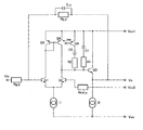
図1に本実施の形態1における増幅装置の構成の一例を示す。
以下、本実施の形態2における光ディスクドライブ装置について説明する。
本実施の形態2における光ディスクドライブ装置は、装着された光ディスクからの反射光量に応じた電流信号を生成する複数の受光素子PDと、各受光素子PDからの電流信号をそれぞれ電圧信号に変換する複数の電流電圧変換部と、各電流電圧変換部からの電圧信号を用いて演算を行う演算部と、を有する光ディスクドライブ装置用光電気変換ICの電流電圧変換部もしくは演算部のいずれかを実施の形態1で説明した増幅装置を用いて構成する点に特徴がある。
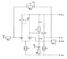
図16に本実施の形態3における光ディスクドライブ装置用光電気変換ICに含まれる電流電圧変換部の構成例を示す。この電流電圧変換部は、図14に示す電流電圧変換部に対して、装着された光ディスクの種類(メディアタイプ)によってゲインの切り換えが可能となっており、反射率の異なるディスクに対して同等の出力電圧レベルを得ることができる。
Rg_a〜Rg_c、Rref_a、R1〜R3、Rf 抵抗
C_a、C_c、C1〜C3、Cf コンデンサ
I1〜I6 定電流源
PD、PDi 受光素子
T−sw サーミスタ
Api アンプ
11 電流−電圧変換用差動増幅回路
12 位相補償部
13 出力回路
14 アナログスイッチ回路
Claims (9)
- 入力信号を入力する差動入力部と、電源ラインと、前記差動入力部からの信号を送信する信号ラインと、前記電源ラインと前記信号ラインとの間に設けられた複数の位相補償回路を有し前記差動入力部からの信号に位相補償を施す位相補償部と、前記信号ラインに接続し前記位相補償部が位相補償を施した信号を入力する出力部と、前記出力部の出力を前記差動入力部へ帰還する帰還抵抗部と、を備え、前記入力信号を前記帰還抵抗部の抵抗値で決まる所定の増幅率で増幅した信号を前記出力部から出力する増幅装置であって、
前記位相補償回路の容量値を形成するコンデンサと前記電源ラインとの間に設けられスイッチ動作して前記位相補償部の抵抗値ないし容量値を切り換えるバイポーラトランジスタと、
前記バイポーラトランジスタと前記コンデンサとの間に接続し前記バイポーラトランジスタのスイッチ動作に連動して動作して前記バイポーラトランジスタのオン時に前記バイポーラトランジスタを能動領域で動作させる電流源を具備する
ことを特徴とする増幅装置。 - 請求項1に記載の増幅装置において、
前記電源ラインは正の電源ラインないし接地電源ラインであり、
前記位相補償回路は前記信号ラインと前記正の電源ラインないし接地電源ラインとの間に設けられる
ことを特徴とする増幅装置。 - 請求項1に記載の増幅装置において、
前記電源ラインは正の電源ラインおよび接地電源ラインであり、
前記位相補償回路を前記信号ラインと前記正の電源ラインの間および前記信号ラインと前記接地電源ラインの間それぞれに設け、且つ前記各位相補償回路すべてに対して前記バイポーラトランジスタを設けて、
前記正の電源ラインに接続する位相補償回路と前記接地電源ラインに接続する位相補償回路を前記バイポーラトランジスタにより選択可能にした
ことを特徴とする増幅装置。 - 請求項1ないし3のいずれかに記載の増幅装置において、前記バイポーラトランジスタのベースにローパスフィルタをさらに設けたことを特徴とする増幅装置。
- 複数のメディアタイプの光ディスクに対応できる光ディスクドライブ装置において、
装着された光ディスクからの反射光量に応じた電流信号を生成する複数の受光素子と、前記各受光素子からの電流信号をそれぞれ電圧信号に変換する複数の電流電圧変換部と、前記各電流電圧変換部からの電圧信号を用いて演算を行う演算部と、を有してなる光電気変換器内の前記電流電圧変換部もしくは前記演算部を、請求項1ないし4のいずれかに記載の増幅装置を用いて構成したことを特徴とする光ディスクドライブ装置。 - 請求項5記載の光ディスクドライブ装置において、
前記増幅装置の帰還抵抗部を抵抗値の切り換えが可能な回路にするとともに、
装着された光ディスクのメディアタイプを判別する機構と、メディアタイプの判別結果を基に、反射率の高い光ディスクである場合には前記帰還抵抗部の抵抗値を小さくし、反射率の低い光ディスクである場合には前記帰還抵抗部の抵抗値を大きくする機構と、をさらに設けた
ことを特徴とする光ディスクドライブ装置。 - 請求項6記載の光ディスクドライブ装置において、
装着された光ディスクのメディアタイプの判別結果を基に、前記増幅装置の差動入力部内蔵の入力信号を入力するトランジスタのバイアス電流値を調整する機構をさらに設けた
ことを特徴とする光ディスクドライブ装置。 - 請求項5ないし7のいずれかに記載の光ディスクドライブ装置において、
前記増幅装置の位相補償部の抵抗値ないし容量値を切り換えるバイポーラトランジスタに温度の変動に連動してスイッチ動作させる機構をさらに設けた
ことを特徴とする光ディスクドライブ装置。 - 請求項5ないし8のいずれかに記載の光ディスクドライブ装置において、
前記増幅装置の位相補償部の容量値ないし抵抗値を切り換えることにより、光ディスクへのデータ書き込み時には、光ディスクからのデータ読み込み時よりも前記増幅装置の出力信号の群遅延偏差を小さくし、光ディスクからのデータ読み込み時には、光ディスクへのデータ書き込み時よりも前記増幅装置の出力信号のカットオフ周波数を高くする
ことを特徴とする光ディスクドライブ装置。
Priority Applications (2)
| Application Number | Priority Date | Filing Date | Title |
|---|---|---|---|
| JP2006027813A JP4884018B2 (ja) | 2005-05-12 | 2006-02-06 | 増幅装置、および光ディスクドライブ装置 |
| US11/430,241 US7391265B2 (en) | 2005-05-12 | 2006-05-09 | Amplifier unit and optical disc drive |
Applications Claiming Priority (3)
| Application Number | Priority Date | Filing Date | Title |
|---|---|---|---|
| JP2005139189 | 2005-05-12 | ||
| JP2005139189 | 2005-05-12 | ||
| JP2006027813A JP4884018B2 (ja) | 2005-05-12 | 2006-02-06 | 増幅装置、および光ディスクドライブ装置 |
Publications (2)
| Publication Number | Publication Date |
|---|---|
| JP2006345481A JP2006345481A (ja) | 2006-12-21 |
| JP4884018B2 true JP4884018B2 (ja) | 2012-02-22 |
Family
ID=36970187
Family Applications (1)
| Application Number | Title | Priority Date | Filing Date |
|---|---|---|---|
| JP2006027813A Expired - Fee Related JP4884018B2 (ja) | 2005-05-12 | 2006-02-06 | 増幅装置、および光ディスクドライブ装置 |
Country Status (2)
| Country | Link |
|---|---|
| US (1) | US7391265B2 (ja) |
| JP (1) | JP4884018B2 (ja) |
Families Citing this family (13)
| Publication number | Priority date | Publication date | Assignee | Title |
|---|---|---|---|---|
| JP4687699B2 (ja) * | 2007-09-27 | 2011-05-25 | Tdk株式会社 | 増幅回路及びこれを備える光ピックアップ |
| JP2009088583A (ja) * | 2007-09-27 | 2009-04-23 | Tdk Corp | 増幅回路及びこれを備える光ピックアップ |
| JP4807369B2 (ja) * | 2008-03-17 | 2011-11-02 | Tdk株式会社 | 光電流・電圧変換回路 |
| JP5081678B2 (ja) | 2008-03-24 | 2012-11-28 | 株式会社日立製作所 | 光信号受信回路 |
| JP5110017B2 (ja) * | 2009-03-26 | 2012-12-26 | Tdk株式会社 | 増幅回路及びこれを備える光ピックアップ |
| JP5169941B2 (ja) * | 2009-03-26 | 2013-03-27 | Tdk株式会社 | 増幅回路及びこれを備える光ピックアップ |
| JP4643728B2 (ja) * | 2009-05-26 | 2011-03-02 | 徹 川名 | オペアンプ |
| JP2013030950A (ja) * | 2011-07-28 | 2013-02-07 | New Japan Radio Co Ltd | 演算増幅器 |
| US9492144B1 (en) | 2015-12-02 | 2016-11-15 | Butterfly Network, Inc. | Multi-level pulser and related apparatus and methods |
| US10187020B2 (en) * | 2015-12-02 | 2019-01-22 | Butterfly Network, Inc. | Trans-impedance amplifier for ultrasound device and related apparatus and methods |
| US10082488B2 (en) | 2015-12-02 | 2018-09-25 | Butterfly Network, Inc. | Time gain compensation circuit and related apparatus and methods |
| TW202034624A (zh) | 2018-11-09 | 2020-09-16 | 美商蝴蝶網路公司 | 用於超音波裝置的跨阻抗放大器(tia) |
| FR3118549B1 (fr) * | 2020-12-28 | 2025-10-31 | Easii Ic | Amplificateur de transimpédance programmable |
Family Cites Families (13)
| Publication number | Priority date | Publication date | Assignee | Title |
|---|---|---|---|---|
| US3327235A (en) * | 1964-05-28 | 1967-06-20 | Westinghouse Electric Corp | Dc amplifier having single time delay characteristic |
| JPH06101654B2 (ja) * | 1986-02-20 | 1994-12-12 | ロ−ム株式会社 | 録音・再生装置 |
| JPH0286210A (ja) * | 1988-09-21 | 1990-03-27 | Toyota Autom Loom Works Ltd | トランジスタの異常検出回路 |
| JPH06113393A (ja) * | 1992-09-28 | 1994-04-22 | Sony Corp | ステレオ受信機 |
| JP3142214B2 (ja) * | 1994-11-28 | 2001-03-07 | シャープ株式会社 | 受光増幅装置 |
| US6016301A (en) * | 1996-04-01 | 2000-01-18 | Sony Corporation | Optical pickup device and optical disc reproducing apparatus |
| JPH10107563A (ja) | 1996-09-27 | 1998-04-24 | Sharp Corp | アナログスイッチ回路およびこれを用いた受光増幅装置 |
| JPH10290127A (ja) * | 1997-04-17 | 1998-10-27 | Rohm Co Ltd | 電流/電圧変換ic及び光電気変換ic |
| US6066985A (en) * | 1998-09-10 | 2000-05-23 | Seiko Epson Corporation | Large swing input/output analog buffer |
| US6753734B2 (en) * | 2001-06-06 | 2004-06-22 | Anadigics, Inc. | Multi-mode amplifier bias circuit |
| JP4713022B2 (ja) * | 2001-07-05 | 2011-06-29 | パナソニック株式会社 | 光ディスクドライブ装置用の増幅回路 |
| JP2003234623A (ja) * | 2002-02-12 | 2003-08-22 | Sharp Corp | 受光アンプ回路及びこれを用いた光ピックアップ |
| JP4680815B2 (ja) * | 2006-03-31 | 2011-05-11 | パナソニック株式会社 | 増幅回路および光ピックアップ |
-
2006
- 2006-02-06 JP JP2006027813A patent/JP4884018B2/ja not_active Expired - Fee Related
- 2006-05-09 US US11/430,241 patent/US7391265B2/en not_active Expired - Fee Related
Also Published As
| Publication number | Publication date |
|---|---|
| US20060202761A1 (en) | 2006-09-14 |
| US7391265B2 (en) | 2008-06-24 |
| JP2006345481A (ja) | 2006-12-21 |
Similar Documents
| Publication | Publication Date | Title |
|---|---|---|
| JP4884018B2 (ja) | 増幅装置、および光ディスクドライブ装置 | |
| US7449670B2 (en) | Amplifier circuit and optical pickup device | |
| JP2010011141A (ja) | ピークホールド回路 | |
| JPH10290127A (ja) | 電流/電圧変換ic及び光電気変換ic | |
| US8055139B2 (en) | Light receiver | |
| US6396351B1 (en) | Preamplifier circuit for a photodetector | |
| US7714269B2 (en) | Light receiving circuit | |
| US7245188B2 (en) | Light receiving amplification circuit | |
| US7427738B2 (en) | Light-receiving amplifier and optical pickup device | |
| JP2010136030A (ja) | 受光増幅回路および光ディスク装置 | |
| JP2007028372A (ja) | 受光増幅回路およびそれを用いた光ピックアップ装置 | |
| JP3535029B2 (ja) | 受光増幅回路 | |
| JP4837585B2 (ja) | 受光回路 | |
| JP2005252810A (ja) | 電流電圧変換回路 | |
| JP2008277915A (ja) | 光電変換装置 | |
| CN100452198C (zh) | 信号驱动装置及使用该信号驱动装置的光学拾取装置 | |
| JP3922906B2 (ja) | 広帯域差動増幅回路 | |
| JP2007294492A (ja) | 光電変換装置 | |
| JP2008306673A (ja) | 増幅回路 | |
| US20090008535A1 (en) | Differential amplifier circuit, operational amplifier circuit, light-receiving amplifier circuit using the same, function selection circuit, and light-receiving circuit using the same | |
| JP2010041272A (ja) | 非反転増幅器、受光増幅素子および光ピックアップ素子 | |
| JP4641000B2 (ja) | 受光アンプ回路および光ピックアップ | |
| JP2005303684A (ja) | 利得可変増幅回路および光ピックアップ装置 | |
| JP2009289369A (ja) | 光電変換装置 | |
| JP2007013451A (ja) | スイッチ回路、受光増幅回路及び光ピックアップ装置 |
Legal Events
| Date | Code | Title | Description |
|---|---|---|---|
| RD04 | Notification of resignation of power of attorney |
Free format text: JAPANESE INTERMEDIATE CODE: A7424 Effective date: 20080430 |
|
| A621 | Written request for application examination |
Free format text: JAPANESE INTERMEDIATE CODE: A621 Effective date: 20080612 |
|
| A977 | Report on retrieval |
Free format text: JAPANESE INTERMEDIATE CODE: A971007 Effective date: 20100527 |
|
| A131 | Notification of reasons for refusal |
Free format text: JAPANESE INTERMEDIATE CODE: A131 Effective date: 20100608 |
|
| A521 | Request for written amendment filed |
Free format text: JAPANESE INTERMEDIATE CODE: A523 Effective date: 20100805 |
|
| A131 | Notification of reasons for refusal |
Free format text: JAPANESE INTERMEDIATE CODE: A131 Effective date: 20110322 |
|
| TRDD | Decision of grant or rejection written | ||
| A01 | Written decision to grant a patent or to grant a registration (utility model) |
Free format text: JAPANESE INTERMEDIATE CODE: A01 Effective date: 20111108 |
|
| A01 | Written decision to grant a patent or to grant a registration (utility model) |
Free format text: JAPANESE INTERMEDIATE CODE: A01 |
|
| A61 | First payment of annual fees (during grant procedure) |
Free format text: JAPANESE INTERMEDIATE CODE: A61 Effective date: 20111206 |
|
| FPAY | Renewal fee payment (event date is renewal date of database) |
Free format text: PAYMENT UNTIL: 20141216 Year of fee payment: 3 |
|
| FPAY | Renewal fee payment (event date is renewal date of database) |
Free format text: PAYMENT UNTIL: 20141216 Year of fee payment: 3 |
|
| LAPS | Cancellation because of no payment of annual fees |