JP4900623B2 - 複合バラン - Google Patents
複合バラン Download PDFInfo
- Publication number
- JP4900623B2 JP4900623B2 JP2009126349A JP2009126349A JP4900623B2 JP 4900623 B2 JP4900623 B2 JP 4900623B2 JP 2009126349 A JP2009126349 A JP 2009126349A JP 2009126349 A JP2009126349 A JP 2009126349A JP 4900623 B2 JP4900623 B2 JP 4900623B2
- Authority
- JP
- Japan
- Prior art keywords
- line
- coupled
- balun
- coupling line
- dielectric layer
- Prior art date
- Legal status (The legal status is an assumption and is not a legal conclusion. Google has not performed a legal analysis and makes no representation as to the accuracy of the status listed.)
- Active
Links
- 150000001875 compounds Chemical class 0.000 title 1
- 230000008878 coupling Effects 0.000 claims description 138
- 238000010168 coupling process Methods 0.000 claims description 138
- 238000005859 coupling reaction Methods 0.000 claims description 138
- 239000004020 conductor Substances 0.000 claims description 44
- 239000003990 capacitor Substances 0.000 claims description 43
- 239000002131 composite material Substances 0.000 claims description 37
- 230000005540 biological transmission Effects 0.000 description 16
- 239000000919 ceramic Substances 0.000 description 12
- 239000003989 dielectric material Substances 0.000 description 4
- 238000010586 diagram Methods 0.000 description 3
- 238000010295 mobile communication Methods 0.000 description 3
- 230000000694 effects Effects 0.000 description 2
- 238000004891 communication Methods 0.000 description 1
- 238000010304 firing Methods 0.000 description 1
- 238000010030 laminating Methods 0.000 description 1
- 238000004519 manufacturing process Methods 0.000 description 1
- 238000000034 method Methods 0.000 description 1
- 238000012986 modification Methods 0.000 description 1
- 230000004048 modification Effects 0.000 description 1
- 230000008569 process Effects 0.000 description 1
- 230000009467 reduction Effects 0.000 description 1
- 238000005549 size reduction Methods 0.000 description 1
- 229910000679 solder Inorganic materials 0.000 description 1
- 125000006850 spacer group Chemical group 0.000 description 1
- 239000000758 substrate Substances 0.000 description 1
Images


Landscapes
- Coils Or Transformers For Communication (AREA)
Description
(a)電力増幅器や、無線周波数集積回路に直流電圧を供給する必要がある場合に有用な複合バランを提供することができる。
(b)電力増幅器や、無線周波数集積回路に直流電圧を供給する必要がある場合に、電源供給回路を経由して侵入するノイズを阻止しえる複合バランを提供することができる。
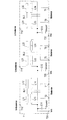
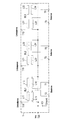
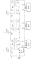
L11、L21、L31 第1結合線路
L12、L22、L32 第2結合線路
L13、L23、L33 第3結合線路
L14、L24、L34 第4結合線路
C1、C11、C12、C13 キャパシタ
Claims (2)
- 複数個のバランと、少なくとも1つのキャパシタと、直流電圧供給端子とを含む複合バランであって、
前記複数個のバラン及び前記キャパシタは、1つのチップ内に内蔵されており、
前記バランのそれぞれは、第1乃至第4結合線路と、第1平衡端子と、第2平衡端子と、不平衡端子とを含んでおり、
前記第1結合線路は、一端が前記不平衡端子に接続されており、
前記第2結合線路は、一端が前記第1結合線路の他端に接続されており、
前記第3結合線路は、前記第1結合線路に電磁結合し、一端が前記第1平衡端子に接続され、他端が前記直流電圧供給端子に接続されており、
前記第4結合線路は、前記第2結合線路に電磁結合し、一端が前記第2平衡端子に接続され、他端が前記直流電圧供給端子に接続されており、
前記キャパシタは、一端が、前記直流電圧供給端子に接続され、他端が接地端子に導かれており、
前記バランのそれぞれは、前記第1結合線路及び前記第2結合線路と、前記第3結合線路及び前記第4結合線路とが、前記チップを構成する誘電体層を介して電磁結合しており、
前記複数のバランの間では、
前記第1結合線路及び前記第2結合線路を構成するストリップ状導体が、互いに間隔を隔てて一方向に横並びに配置され、
前記第3結合線路及び前記第4結合線路を構成するストリップ状導体が、互いに間隔を隔てて一方向に横並びに配置されており、
前記第1平衡端子、第2平衡端子及び不平衡端子は、最下層の誘電体層の下面の周辺部に、間隔を隔てて配置されており、
前記不平衡端子は、前記最下層の誘電体層の一辺に配置されており、
前記第1平衡端子及び第2平衡端子は、前記最下層の誘電体層の前記一辺と向き合う他の辺に配置されている、
バラン。 - 請求項1に記載された複合バランであって、前記キャパシタは、前記複数のバランにおいて、共用されている、バラン。
Priority Applications (2)
| Application Number | Priority Date | Filing Date | Title |
|---|---|---|---|
| JP2009126349A JP4900623B2 (ja) | 2009-05-26 | 2009-05-26 | 複合バラン |
| US12/774,972 US8324981B2 (en) | 2009-05-26 | 2010-05-06 | Composite balun |
Applications Claiming Priority (1)
| Application Number | Priority Date | Filing Date | Title |
|---|---|---|---|
| JP2009126349A JP4900623B2 (ja) | 2009-05-26 | 2009-05-26 | 複合バラン |
Publications (2)
| Publication Number | Publication Date |
|---|---|
| JP2010278514A JP2010278514A (ja) | 2010-12-09 |
| JP4900623B2 true JP4900623B2 (ja) | 2012-03-21 |
Family
ID=43425108
Family Applications (1)
| Application Number | Title | Priority Date | Filing Date |
|---|---|---|---|
| JP2009126349A Active JP4900623B2 (ja) | 2009-05-26 | 2009-05-26 | 複合バラン |
Country Status (1)
| Country | Link |
|---|---|
| JP (1) | JP4900623B2 (ja) |
Family Cites Families (2)
| Publication number | Priority date | Publication date | Assignee | Title |
|---|---|---|---|---|
| JP4783996B2 (ja) * | 2001-05-02 | 2011-09-28 | 株式会社村田製作所 | 積層型複合バラントランス |
| JP3770883B2 (ja) * | 2003-04-17 | 2006-04-26 | 双信電機株式会社 | 受動部品 |
-
2009
- 2009-05-26 JP JP2009126349A patent/JP4900623B2/ja active Active
Also Published As
| Publication number | Publication date |
|---|---|
| JP2010278514A (ja) | 2010-12-09 |
Similar Documents
| Publication | Publication Date | Title |
|---|---|---|
| CN105453429B (zh) | 高频模块 | |
| CN103038937B (zh) | 定向耦合器 | |
| TW201644191A (zh) | 包含線圈及電容的層積複合電子零件 | |
| JP5800113B2 (ja) | 高周波モジュール部品 | |
| JP2009153106A (ja) | バンドパスフィルタ、高周波部品および通信装置 | |
| JP6687105B2 (ja) | 電子部品 | |
| JPWO2015129597A1 (ja) | 積層型コイル素子、アンテナモジュール、および、無線通信モジュール | |
| CN105453430A (zh) | 高频模块 | |
| JP2006094462A (ja) | 積層型バルントランス | |
| JP2004304615A (ja) | 高周波複合部品 | |
| JP2008182598A (ja) | 左手系伝送線路、ハイパスフィルタおよび通信装置 | |
| US8324981B2 (en) | Composite balun | |
| KR101983139B1 (ko) | 적층형 인덕터 및 적층형 인덕터 어레이 | |
| WO2010087302A1 (ja) | アンテナ共用モジュール | |
| JP4900623B2 (ja) | 複合バラン | |
| JP2003087074A (ja) | 積層型フィルタ | |
| JP2001267141A (ja) | ローパスフィルタ | |
| JP3153518U (ja) | 複合バラン | |
| JP4401981B2 (ja) | フィルタ | |
| JP2001185972A (ja) | 積層フィルタ | |
| KR100550843B1 (ko) | 초소형 적층형 평형 필터 | |
| JP5835475B2 (ja) | 高周波フィルタ | |
| US12519449B2 (en) | Multilayer electronic component | |
| JP4086154B2 (ja) | 高周波複合部品 | |
| CN115811290A (zh) | 层叠型电子部件 |
Legal Events
| Date | Code | Title | Description |
|---|---|---|---|
| A977 | Report on retrieval |
Free format text: JAPANESE INTERMEDIATE CODE: A971007 Effective date: 20110404 |
|
| A131 | Notification of reasons for refusal |
Free format text: JAPANESE INTERMEDIATE CODE: A131 Effective date: 20110525 |
|
| A521 | Request for written amendment filed |
Free format text: JAPANESE INTERMEDIATE CODE: A523 Effective date: 20110721 |
|
| A02 | Decision of refusal |
Free format text: JAPANESE INTERMEDIATE CODE: A02 Effective date: 20110810 |
|
| A521 | Request for written amendment filed |
Free format text: JAPANESE INTERMEDIATE CODE: A523 Effective date: 20111107 |
|
| A911 | Transfer to examiner for re-examination before appeal (zenchi) |
Free format text: JAPANESE INTERMEDIATE CODE: A911 Effective date: 20111114 |
|
| TRDD | Decision of grant or rejection written | ||
| A01 | Written decision to grant a patent or to grant a registration (utility model) |
Free format text: JAPANESE INTERMEDIATE CODE: A01 Effective date: 20111207 |
|
| A01 | Written decision to grant a patent or to grant a registration (utility model) |
Free format text: JAPANESE INTERMEDIATE CODE: A01 |
|
| A61 | First payment of annual fees (during grant procedure) |
Free format text: JAPANESE INTERMEDIATE CODE: A61 Effective date: 20111220 |
|
| R150 | Certificate of patent or registration of utility model |
Ref document number: 4900623 Country of ref document: JP Free format text: JAPANESE INTERMEDIATE CODE: R150 Free format text: JAPANESE INTERMEDIATE CODE: R150 |
|
| FPAY | Renewal fee payment (event date is renewal date of database) |
Free format text: PAYMENT UNTIL: 20150113 Year of fee payment: 3 |
|
| R250 | Receipt of annual fees |
Free format text: JAPANESE INTERMEDIATE CODE: R250 |