JP4941509B2 - 電子制御装置 - Google Patents
電子制御装置 Download PDFInfo
- Publication number
- JP4941509B2 JP4941509B2 JP2009132257A JP2009132257A JP4941509B2 JP 4941509 B2 JP4941509 B2 JP 4941509B2 JP 2009132257 A JP2009132257 A JP 2009132257A JP 2009132257 A JP2009132257 A JP 2009132257A JP 4941509 B2 JP4941509 B2 JP 4941509B2
- Authority
- JP
- Japan
- Prior art keywords
- circuit board
- mold resin
- stress
- electronic control
- outer edge
- Prior art date
- Legal status (The legal status is an assumption and is not a legal conclusion. Google has not performed a legal analysis and makes no representation as to the accuracy of the status listed.)
- Expired - Fee Related
Links
Images




Classifications
-
- H—ELECTRICITY
- H05—ELECTRIC TECHNIQUES NOT OTHERWISE PROVIDED FOR
- H05K—PRINTED CIRCUITS; CASINGS OR CONSTRUCTIONAL DETAILS OF ELECTRIC APPARATUS; MANUFACTURE OF ASSEMBLAGES OF ELECTRICAL COMPONENTS
- H05K7/00—Constructional details common to different types of electric apparatus
- H05K7/20—Modifications to facilitate cooling, ventilating, or heating
- H05K7/2039—Modifications to facilitate cooling, ventilating, or heating characterised by the heat transfer by conduction from the heat generating element to a dissipating body
- H05K7/20436—Inner thermal coupling elements in heat dissipating housings, e.g. protrusions or depressions integrally formed in the housing
- H05K7/20445—Inner thermal coupling elements in heat dissipating housings, e.g. protrusions or depressions integrally formed in the housing the coupling element being an additional piece, e.g. thermal standoff
- H05K7/20454—Inner thermal coupling elements in heat dissipating housings, e.g. protrusions or depressions integrally formed in the housing the coupling element being an additional piece, e.g. thermal standoff with a conformable or flexible structure compensating for irregularities, e.g. cushion bags, thermal paste
-
- H—ELECTRICITY
- H05—ELECTRIC TECHNIQUES NOT OTHERWISE PROVIDED FOR
- H05K—PRINTED CIRCUITS; CASINGS OR CONSTRUCTIONAL DETAILS OF ELECTRIC APPARATUS; MANUFACTURE OF ASSEMBLAGES OF ELECTRICAL COMPONENTS
- H05K3/00—Apparatus or processes for manufacturing printed circuits
- H05K3/22—Secondary treatment of printed circuits
- H05K3/28—Applying non-metallic protective coatings
- H05K3/284—Applying non-metallic protective coatings for encapsulating mounted components
-
- H—ELECTRICITY
- H05—ELECTRIC TECHNIQUES NOT OTHERWISE PROVIDED FOR
- H05K—PRINTED CIRCUITS; CASINGS OR CONSTRUCTIONAL DETAILS OF ELECTRIC APPARATUS; MANUFACTURE OF ASSEMBLAGES OF ELECTRICAL COMPONENTS
- H05K5/00—Casings, cabinets or drawers for electric apparatus
- H05K5/06—Hermetically-sealed casings
- H05K5/065—Hermetically-sealed casings sealed by encapsulation, e.g. waterproof resin forming an integral casing, injection moulding
-
- H—ELECTRICITY
- H05—ELECTRIC TECHNIQUES NOT OTHERWISE PROVIDED FOR
- H05K—PRINTED CIRCUITS; CASINGS OR CONSTRUCTIONAL DETAILS OF ELECTRIC APPARATUS; MANUFACTURE OF ASSEMBLAGES OF ELECTRICAL COMPONENTS
- H05K1/00—Printed circuits
- H05K1/02—Details
- H05K1/0271—Arrangements for reducing stress or warp in rigid printed circuit boards, e.g. caused by loads, vibrations or differences in thermal expansion
-
- H—ELECTRICITY
- H05—ELECTRIC TECHNIQUES NOT OTHERWISE PROVIDED FOR
- H05K—PRINTED CIRCUITS; CASINGS OR CONSTRUCTIONAL DETAILS OF ELECTRIC APPARATUS; MANUFACTURE OF ASSEMBLAGES OF ELECTRICAL COMPONENTS
- H05K1/00—Printed circuits
- H05K1/02—Details
- H05K1/09—Use of materials for the conductive, e.g. metallic pattern
- H05K1/092—Dispersed materials, e.g. conductive pastes or inks
- H05K1/095—Dispersed materials, e.g. conductive pastes or inks for polymer thick films, i.e. having a permanent organic polymeric binder
-
- H—ELECTRICITY
- H05—ELECTRIC TECHNIQUES NOT OTHERWISE PROVIDED FOR
- H05K—PRINTED CIRCUITS; CASINGS OR CONSTRUCTIONAL DETAILS OF ELECTRIC APPARATUS; MANUFACTURE OF ASSEMBLAGES OF ELECTRICAL COMPONENTS
- H05K2201/00—Indexing scheme relating to printed circuits covered by H05K1/00
- H05K2201/09—Shape and layout
- H05K2201/09145—Edge details
-
- H—ELECTRICITY
- H05—ELECTRIC TECHNIQUES NOT OTHERWISE PROVIDED FOR
- H05K—PRINTED CIRCUITS; CASINGS OR CONSTRUCTIONAL DETAILS OF ELECTRIC APPARATUS; MANUFACTURE OF ASSEMBLAGES OF ELECTRICAL COMPONENTS
- H05K2201/00—Indexing scheme relating to printed circuits covered by H05K1/00
- H05K2201/09—Shape and layout
- H05K2201/09209—Shape and layout details of conductors
- H05K2201/09654—Shape and layout details of conductors covering at least two types of conductors provided for in H05K2201/09218 - H05K2201/095
- H05K2201/09781—Dummy conductors, i.e. not used for normal transport of current; Dummy electrodes of components
-
- H—ELECTRICITY
- H05—ELECTRIC TECHNIQUES NOT OTHERWISE PROVIDED FOR
- H05K—PRINTED CIRCUITS; CASINGS OR CONSTRUCTIONAL DETAILS OF ELECTRIC APPARATUS; MANUFACTURE OF ASSEMBLAGES OF ELECTRICAL COMPONENTS
- H05K2201/00—Indexing scheme relating to printed circuits covered by H05K1/00
- H05K2201/10—Details of components or other objects attached to or integrated in a printed circuit board
- H05K2201/10227—Other objects, e.g. metallic pieces
- H05K2201/10287—Metal wires as connectors or conductors
-
- H—ELECTRICITY
- H05—ELECTRIC TECHNIQUES NOT OTHERWISE PROVIDED FOR
- H05K—PRINTED CIRCUITS; CASINGS OR CONSTRUCTIONAL DETAILS OF ELECTRIC APPARATUS; MANUFACTURE OF ASSEMBLAGES OF ELECTRICAL COMPONENTS
- H05K2203/00—Indexing scheme relating to apparatus or processes for manufacturing printed circuits covered by H05K3/00
- H05K2203/04—Soldering or other types of metallurgic bonding
- H05K2203/049—Wire bonding
-
- H—ELECTRICITY
- H05—ELECTRIC TECHNIQUES NOT OTHERWISE PROVIDED FOR
- H05K—PRINTED CIRCUITS; CASINGS OR CONSTRUCTIONAL DETAILS OF ELECTRIC APPARATUS; MANUFACTURE OF ASSEMBLAGES OF ELECTRICAL COMPONENTS
- H05K2203/00—Indexing scheme relating to apparatus or processes for manufacturing printed circuits covered by H05K3/00
- H05K2203/13—Moulding and encapsulation; Deposition techniques; Protective layers
- H05K2203/1305—Moulding and encapsulation
- H05K2203/1316—Moulded encapsulation of mounted components
-
- H—ELECTRICITY
- H05—ELECTRIC TECHNIQUES NOT OTHERWISE PROVIDED FOR
- H05K—PRINTED CIRCUITS; CASINGS OR CONSTRUCTIONAL DETAILS OF ELECTRIC APPARATUS; MANUFACTURE OF ASSEMBLAGES OF ELECTRICAL COMPONENTS
- H05K3/00—Apparatus or processes for manufacturing printed circuits
- H05K3/30—Assembling printed circuits with electric components, e.g. with resistors
- H05K3/32—Assembling printed circuits with electric components, e.g. with resistors electrically connecting electric components or wires to printed circuits
- H05K3/321—Assembling printed circuits with electric components, e.g. with resistors electrically connecting electric components or wires to printed circuits by conductive adhesives
-
- H—ELECTRICITY
- H10—SEMICONDUCTOR DEVICES; ELECTRIC SOLID-STATE DEVICES NOT OTHERWISE PROVIDED FOR
- H10W—GENERIC PACKAGES, INTERCONNECTIONS, CONNECTORS OR OTHER CONSTRUCTIONAL DETAILS OF DEVICES COVERED BY CLASS H10
- H10W72/00—Interconnections or connectors in packages
- H10W72/071—Connecting or disconnecting
- H10W72/075—Connecting or disconnecting of bond wires
- H10W72/07551—Connecting or disconnecting of bond wires characterised by changes in properties of the bond wires during the connecting
- H10W72/07552—Connecting or disconnecting of bond wires characterised by changes in properties of the bond wires during the connecting changes in structures or sizes
-
- H—ELECTRICITY
- H10—SEMICONDUCTOR DEVICES; ELECTRIC SOLID-STATE DEVICES NOT OTHERWISE PROVIDED FOR
- H10W—GENERIC PACKAGES, INTERCONNECTIONS, CONNECTORS OR OTHER CONSTRUCTIONAL DETAILS OF DEVICES COVERED BY CLASS H10
- H10W72/00—Interconnections or connectors in packages
- H10W72/50—Bond wires
- H10W72/521—Structures or relative sizes of bond wires
- H10W72/527—Multiple bond wires having different sizes
-
- H—ELECTRICITY
- H10—SEMICONDUCTOR DEVICES; ELECTRIC SOLID-STATE DEVICES NOT OTHERWISE PROVIDED FOR
- H10W—GENERIC PACKAGES, INTERCONNECTIONS, CONNECTORS OR OTHER CONSTRUCTIONAL DETAILS OF DEVICES COVERED BY CLASS H10
- H10W72/00—Interconnections or connectors in packages
- H10W72/50—Bond wires
- H10W72/551—Materials of bond wires
- H10W72/552—Materials of bond wires comprising metals or metalloids, e.g. silver
- H10W72/5522—Materials of bond wires comprising metals or metalloids, e.g. silver comprising gold [Au]
-
- H—ELECTRICITY
- H10—SEMICONDUCTOR DEVICES; ELECTRIC SOLID-STATE DEVICES NOT OTHERWISE PROVIDED FOR
- H10W—GENERIC PACKAGES, INTERCONNECTIONS, CONNECTORS OR OTHER CONSTRUCTIONAL DETAILS OF DEVICES COVERED BY CLASS H10
- H10W72/00—Interconnections or connectors in packages
- H10W72/50—Bond wires
- H10W72/551—Materials of bond wires
- H10W72/552—Materials of bond wires comprising metals or metalloids, e.g. silver
- H10W72/5524—Materials of bond wires comprising metals or metalloids, e.g. silver comprising aluminium [Al]
-
- H—ELECTRICITY
- H10—SEMICONDUCTOR DEVICES; ELECTRIC SOLID-STATE DEVICES NOT OTHERWISE PROVIDED FOR
- H10W—GENERIC PACKAGES, INTERCONNECTIONS, CONNECTORS OR OTHER CONSTRUCTIONAL DETAILS OF DEVICES COVERED BY CLASS H10
- H10W72/00—Interconnections or connectors in packages
- H10W72/851—Dispositions of multiple connectors or interconnections
- H10W72/874—On different surfaces
- H10W72/884—Die-attach connectors and bond wires
-
- H—ELECTRICITY
- H10—SEMICONDUCTOR DEVICES; ELECTRIC SOLID-STATE DEVICES NOT OTHERWISE PROVIDED FOR
- H10W—GENERIC PACKAGES, INTERCONNECTIONS, CONNECTORS OR OTHER CONSTRUCTIONAL DETAILS OF DEVICES COVERED BY CLASS H10
- H10W74/00—Encapsulations, e.g. protective coatings
-
- H—ELECTRICITY
- H10—SEMICONDUCTOR DEVICES; ELECTRIC SOLID-STATE DEVICES NOT OTHERWISE PROVIDED FOR
- H10W—GENERIC PACKAGES, INTERCONNECTIONS, CONNECTORS OR OTHER CONSTRUCTIONAL DETAILS OF DEVICES COVERED BY CLASS H10
- H10W90/00—Package configurations
- H10W90/701—Package configurations characterised by the relative positions of pads or connectors relative to package parts
- H10W90/731—Package configurations characterised by the relative positions of pads or connectors relative to package parts of die-attach connectors
- H10W90/734—Package configurations characterised by the relative positions of pads or connectors relative to package parts of die-attach connectors between a chip and a stacked insulating package substrate, interposer or RDL
-
- H—ELECTRICITY
- H10—SEMICONDUCTOR DEVICES; ELECTRIC SOLID-STATE DEVICES NOT OTHERWISE PROVIDED FOR
- H10W—GENERIC PACKAGES, INTERCONNECTIONS, CONNECTORS OR OTHER CONSTRUCTIONAL DETAILS OF DEVICES COVERED BY CLASS H10
- H10W90/00—Package configurations
- H10W90/701—Package configurations characterised by the relative positions of pads or connectors relative to package parts
- H10W90/751—Package configurations characterised by the relative positions of pads or connectors relative to package parts of bond wires
- H10W90/754—Package configurations characterised by the relative positions of pads or connectors relative to package parts of bond wires between a chip and a stacked insulating package substrate, interposer or RDL
Landscapes
- Engineering & Computer Science (AREA)
- Microelectronics & Electronic Packaging (AREA)
- Physics & Mathematics (AREA)
- Thermal Sciences (AREA)
- Manufacturing & Machinery (AREA)
- Structures Or Materials For Encapsulating Or Coating Semiconductor Devices Or Solid State Devices (AREA)
- Cooling Or The Like Of Semiconductors Or Solid State Devices (AREA)
Description
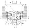
以下、本発明の第1実施形態について図を参照して説明する。本実施形態で示される電子制御装置は、例えば車載用の電子制御装置として用いられるものである。具体的には、自動変速機の電子制御装置として、自動変速機の内部に配置されたバルブボディ内に、ソレノイドや各種センサ等ともに一体化されたモジュールとして取り付けられる。
本実施形態では、第1実施形態と異なる部分についてのみ説明する。図7は、本実施形態に係る電子制御装置1の一部の拡大断面図であり、図2のB部拡大図に相当する図である。
本実施形態では、第1実施形態と異なる部分についてのみ説明する。図8は、本実施形態に係る電子制御装置1の一部の拡大断面図であり、図2のB部拡大図に相当する図である。この図に示されるように、導電性接着剤50は2列に形成されている。そして、各導電性接着剤50が密着補強材60でコーティングされている。
本実施形態では、第1実施形態と異なる部分についてのみ説明する。図9は、本実施形態に係る電子制御装置1の一部の拡大断面図であり、図2のB部拡大図に相当する図である。この図に示されるように、回路基板10には、回路基板10の一面11の外縁部11aにおいて、平面部および側面部によって構成された階段状の段差部19が備えられている。そして、応力緩衝部としての導電性接着剤50が回路基板10の段差部19に設けられ、密着補強材60によってコーティングされている。
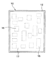
本実施形態では、第1実施形態と異なる部分についてのみ説明する。図10は、本実施形態に係る回路基板10の平面図である。また、図11は、本実施形態に係る電子制御装置1の一部の拡大断面図であり、図2のB部拡大図に相当する図である。
本実施形態では、第5実施形態と異なる部分についてのみ説明する。図14は、本実施形態に係る電子制御装置1の一部の拡大断面図であり、図2のB部拡大図に相当する図である。この図に示されるように、回路基板10には、上述の階段状の段差部19が備えられている。そして、ボンディング部51が回路基板10の段差部19に配置され、ボンディング部51および段差部19が密着補強材60によって覆われている。
本実施形態では、第5実施形態と異なる部分についてのみ説明する。図15は、本実施形態に係る回路基板10の平面図である。この図に示されるように、回路基板10の一面11の外縁部11aにAl等のワイヤ52が配置されている。このワイヤ52は、回路基板10の各辺に沿って直線状に張られている。1本のワイヤ52の長さが例えば15mmであり、2本のワイヤ52がL字状に配置されている。
本実施形態では、上記各実施形態と異なる部分についてのみ説明する。図17は、本実施形態に係る電子制御装置1の一部の拡大断面図であり、図2のB部拡大図に相当する図である。この図に示されるように、回路基板10には、該回路基板10の一面11の外縁部11aに凹部11bが設けられている。そして、密着補強材60は、この凹部11bに埋め尽くされている。これにより、凹部11b内に配置された密着補強材60が厚くなるため、該密着補強材60によってモールド樹脂40の剥離応力を緩和することが可能となる。
本実施形態では、上記各実施形態と異なる部分についてのみ説明する。図18は、本実施形態に係る電子制御装置1の一部の拡大断面図であり、図2のB部拡大図に相当する図である。この図に示されるように、回路基板10には、上述の階段状の段差部19が設けられている。そして、密着補強材60は、段差部19の平面部および側面部によって構成された凹状の角部を覆っている。
第1〜第4実施形態では、導電性接着剤50は回路基板10およびモールド樹脂40よりも弾性率が低いものが用いられていたが、導電性接着剤50は少なくとも回路基板10よりも弾性率が低いものでも良い。すなわち、導電性接着剤50が少なくとも回路基板10よりも軟らかければ、モールド樹脂40から受ける剥離応力が低減されるからである。
11 回路基板の一面
11a 回路基板の一面の外縁部
11b 凹部
12 回路基板の他面
13 電子部品
18 回路基板の側面
19 段差部
20 ベース部材
40 モールド樹脂
50 導電性接着剤
51 ボンディング部
52 ワイヤ
60 密着補強材
Claims (12)
- ヒートシンクとして機能するベース部材(20)と、
一面(11)および該一面(11)の反対側の他面(12)を有し、前記一面(11)に電子部品(13)が搭載され、前記他面(12)に前記ベース部材(20)が接着された回路基板(10)と、
少なくとも、前記ベース部材(20)の前記回路基板(10)が接着された側の面と、前記回路基板(10)を封止したモールド樹脂(40)とを備えた電子制御装置であって、
前記回路基板(10)の一面(11)の少なくとも、外縁部(11a)には、前記一面(11)の外縁部(11a)における前記回路基板(10)の上の部位と前記モールド樹脂(40)との接合部分の応力を、前記一面(11)の外縁部(11a)に前記モールド樹脂(40)が設けられたときの前記一面(11)の外縁部(11a)における前記回路基板(10)の上の部位と前記モールド樹脂(40)との接合部分の応力よりも低くする応力緩衝部(50〜52、60)が備えられており、
前記回路基板(10)は、前記回路基板(10)の一面(11)の外縁部(11a)に、平面部および側面部によって構成された階段状の段差部(19)を備えており、
前記応力緩衝部(50〜52、60)は、前記回路基板(10)よりも弾性率が低いものであり、前記モールド樹脂(40)よりも弾性率が低いものであり、前記回路基板(10)の一面(11)の外縁部(11a)のうち、前記一面(11)の中心から最も離れた場所に配置されており、前記段差部(19)を覆うように配置されていることを特徴とする電子制御装置。 - 前記応力緩衝部は、導電性接着剤(50)であることを特徴とする請求項1に記載の電子制御装置。
- 前記応力緩衝部は、絶縁性樹脂であることを特徴とする請求項1に記載の電子制御装置。
- 前記応力緩衝部は、前記回路基板(10)の一面(11)と該一面(11)に隣接する側面(18)とによって構成された角部を覆うように配置されていることを特徴とする請求項2または3に記載の電子制御装置。
- 前記応力緩衝部は、前記モールド樹脂(40)と前記回路基板(10)とを密着させるための密着補強材(60)でコーティングされていることを特徴とする請求項2ないし4のいずれか1つに記載の電子制御装置。
- 前記応力緩衝部(50〜52、60)は、ワイヤによって形成されると共に前記段差部(19)に配置されたボンディング部(51)と、前記回路基板(10)よりも弾性率が低い密着補強材(60)と、を有して構成されており、
前記密着補強材(60)は前記ボンディング部(51)をコーティングすると共に、前記段差部(19)を覆うように配置されていることを特徴とする請求項1に記載の電子制御装置。 - 前記応力緩衝部(50〜52、60)は、前記段差部(19)に配置されたワイヤ(52)と、前記回路基板(10)よりも弾性率が低い密着補強材(60)と、を有して構成されており、
前記密着補強材(60)は、前記ワイヤ(52)をコーティングすると共に、前記段差部(19)を覆うように配置されていることを特徴とする請求項1に記載の電子制御装置。 - 前記応力緩衝部(50〜52、60)は、前記段差部(19)に配置されたダミー部品と、前記ダミー部品に前記回路基板(10)よりも弾性率が低い密着補強材(60)と、を有して構成されており、
前記密着補強材(60)は前記ダミー部品をコーティングすると共に、前記段差部(19)を覆うように配置されていることを特徴とする請求項1に記載の電子制御装置。 - 前記応力緩衝部(50〜52、60)は、前記回路基板(10)の一面(11)の外縁部(11a)にL字状に配置されていることを特徴とする請求項1ないし8のいずれか1つに記載の電子制御装置。
- 前記応力緩衝部(50〜52、60)は、前記回路基板(10)の一面(11)の外縁部(11a)を一周して囲むように配置されていることを特徴とする請求項1ないし8のいずれか1つに記載の電子制御装置。
- 前記応力緩衝部(50〜52、60)は、前記回路基板(10)の一面(11)の外縁部(11a)に断続的に配置されていることを特徴とする請求項1ないし8のいずれか1つに記載の電子制御装置。
- 前記応力緩衝部(50〜52、60)は、前記回路基板(10)の一面(11)の外縁部(11a)それぞれにドット状に配置されていることを特徴とする請求項1ないし11のいずれか1つに記載の電子制御装置。
Priority Applications (2)
| Application Number | Priority Date | Filing Date | Title |
|---|---|---|---|
| JP2009132257A JP4941509B2 (ja) | 2008-10-20 | 2009-06-01 | 電子制御装置 |
| US12/588,419 US8358514B2 (en) | 2008-10-20 | 2009-10-15 | Electronic control device |
Applications Claiming Priority (3)
| Application Number | Priority Date | Filing Date | Title |
|---|---|---|---|
| JP2008269457 | 2008-10-20 | ||
| JP2008269457 | 2008-10-20 | ||
| JP2009132257A JP4941509B2 (ja) | 2008-10-20 | 2009-06-01 | 電子制御装置 |
Related Child Applications (1)
| Application Number | Title | Priority Date | Filing Date |
|---|---|---|---|
| JP2011096729A Division JP5691794B2 (ja) | 2008-10-20 | 2011-04-25 | 電子制御装置 |
Publications (2)
| Publication Number | Publication Date |
|---|---|
| JP2010123914A JP2010123914A (ja) | 2010-06-03 |
| JP4941509B2 true JP4941509B2 (ja) | 2012-05-30 |
Family
ID=42108502
Family Applications (1)
| Application Number | Title | Priority Date | Filing Date |
|---|---|---|---|
| JP2009132257A Expired - Fee Related JP4941509B2 (ja) | 2008-10-20 | 2009-06-01 | 電子制御装置 |
Country Status (2)
| Country | Link |
|---|---|
| US (1) | US8358514B2 (ja) |
| JP (1) | JP4941509B2 (ja) |
Families Citing this family (24)
| Publication number | Priority date | Publication date | Assignee | Title |
|---|---|---|---|---|
| DE102009002519A1 (de) * | 2009-04-21 | 2010-10-28 | Robert Bosch Gmbh | Gekapselte Schaltungsvorrichtung für Substrate mit Absorptionsschicht sowie Verfahren zu Herstellung derselben |
| JP5211364B2 (ja) * | 2010-05-07 | 2013-06-12 | 三菱電機株式会社 | 半導体装置 |
| JP5602095B2 (ja) | 2011-06-09 | 2014-10-08 | 三菱電機株式会社 | 半導体装置 |
| JP5974428B2 (ja) * | 2011-07-14 | 2016-08-23 | 三菱電機株式会社 | 半導体装置 |
| DE102011088969A1 (de) | 2011-12-19 | 2013-06-20 | Robert Bosch Gmbh | Getriebesteuermodul |
| JP2013131713A (ja) * | 2011-12-22 | 2013-07-04 | Hitachi Automotive Systems Ltd | 制御装置に用いる電子回路装置 |
| JP5692419B2 (ja) * | 2012-01-27 | 2015-04-01 | 株式会社村田製作所 | 多層配線基板 |
| US9312193B2 (en) | 2012-11-09 | 2016-04-12 | Taiwan Semiconductor Manufacturing Company, Ltd. | Stress relief structures in package assemblies |
| DE102013002629A1 (de) * | 2013-02-15 | 2014-08-21 | HKR Seuffer Automotive GmbH & Co. KG | Deckelelement und Gehäusevorrichtung zur Verwendung des Deckelelements |
| JP5999041B2 (ja) * | 2013-07-23 | 2016-09-28 | 株式会社デンソー | 電子装置 |
| WO2015104808A1 (ja) * | 2014-01-09 | 2015-07-16 | 株式会社日立製作所 | パワー半導体装置および電力変換装置 |
| US9560749B2 (en) | 2014-03-17 | 2017-01-31 | Apple Inc. | Electronic devices having stress concentrators for printed circuit boards |
| EP2958139B1 (de) * | 2014-06-18 | 2020-08-05 | Heraeus Deutschland GmbH & Co. KG | Verfahren zur Herstellung eines Halbleitermoduls |
| CN107548573A (zh) * | 2015-07-31 | 2018-01-05 | 惠普发展公司,有限责任合伙企业 | 印刷电路板至模制化合物的接合部 |
| DE102015223415A1 (de) * | 2015-11-26 | 2017-06-01 | Robert Bosch Gmbh | Verfahren zur Herstellung einer elektrischen Vorrichtung mit einer Umhüllmasse |
| KR102319372B1 (ko) * | 2017-04-11 | 2021-11-01 | 삼성전자주식회사 | 생체 센서를 포함하는 전자 장치 |
| DE102017211513A1 (de) * | 2017-07-06 | 2019-01-10 | Robert Bosch Gmbh | Elektronikmodul und Kombination eines Elektronikmoduls mit einer Hydraulikplatte |
| CN110572937B (zh) * | 2018-06-06 | 2022-07-08 | 江西卓讯微电子有限公司 | 传感器 |
| DE102018217456B4 (de) | 2018-10-11 | 2020-07-09 | Conti Temic Microelectronic Gmbh | Elektronische Steuervorrichtung und Verfahren zur Herstellung einer elektronischen Steuervorrichtung |
| IT201800010294A1 (it) * | 2018-11-13 | 2020-05-13 | F A R T S R L | Unita' di alimentazione per esterni |
| KR102438344B1 (ko) * | 2019-10-14 | 2022-09-01 | 세메스 주식회사 | 웨이퍼형 센서 유닛 및 웨이퍼형 센서 유닛의 제조 방법 |
| JP7494521B2 (ja) * | 2020-03-30 | 2024-06-04 | 富士電機株式会社 | 半導体装置及び半導体装置の製造方法 |
| JP2024097134A (ja) * | 2023-01-05 | 2024-07-18 | 三菱電機株式会社 | 半導体装置 |
| WO2024201738A1 (ja) * | 2023-03-28 | 2024-10-03 | 三菱電機株式会社 | 電動機および空気調和機 |
Family Cites Families (19)
| Publication number | Priority date | Publication date | Assignee | Title |
|---|---|---|---|---|
| JPS606558B2 (ja) * | 1977-11-17 | 1985-02-19 | 三菱電機株式会社 | 電子部品の樹脂パツケ−ジ法 |
| JPH05152461A (ja) * | 1991-11-26 | 1993-06-18 | Toshiba Corp | セラミツクス回路基板 |
| JPH0536861A (ja) | 1991-07-30 | 1993-02-12 | Sumitomo Electric Ind Ltd | 半導体デバイス |
| US6107690A (en) * | 1995-09-26 | 2000-08-22 | Micron Technology, Inc. | Coated semiconductor die/leadframe assembly and method for coating the assembly |
| KR100386061B1 (ko) * | 1995-10-24 | 2003-08-21 | 오끼 덴끼 고오교 가부시끼가이샤 | 크랙을방지하기위한개량된구조를가지는반도체장치및리이드프레임 |
| TW330337B (en) * | 1997-05-23 | 1998-04-21 | Siliconware Precision Industries Co Ltd | Semiconductor package with detached die pad |
| JP3835895B2 (ja) | 1997-07-22 | 2006-10-18 | 株式会社デンソー | 半導体装置 |
| CA2255441C (en) * | 1997-12-08 | 2003-08-05 | Hiroki Sekiya | Package for semiconductor power device and method for assembling the same |
| JPH11345905A (ja) * | 1998-06-02 | 1999-12-14 | Mitsubishi Electric Corp | 半導体装置 |
| CN1278402C (zh) * | 2000-06-16 | 2006-10-04 | 松下电器产业株式会社 | 电子器件的封装方法及电子器件封装体 |
| JP2002076201A (ja) | 2000-08-31 | 2002-03-15 | Keihin Corp | 半導体装置の実装構造および実装方法 |
| WO2004004005A1 (ja) * | 2002-07-01 | 2004-01-08 | Renesas Technology Corp. | 半導体装置およびその製造方法 |
| JP4283514B2 (ja) * | 2002-09-24 | 2009-06-24 | 株式会社日立製作所 | 電子回路装置 |
| US7176563B2 (en) * | 2003-09-18 | 2007-02-13 | International Business Machine Corporation | Electronically grounded heat spreader |
| JP4283741B2 (ja) | 2004-07-26 | 2009-06-24 | 株式会社日立製作所 | 樹脂モールド型モジュールとその製造方法 |
| JP4821537B2 (ja) * | 2006-09-26 | 2011-11-24 | 株式会社デンソー | 電子制御装置 |
| JP2008141122A (ja) * | 2006-12-05 | 2008-06-19 | Denso Corp | 樹脂モールド電子部品及びその製造方法 |
| JP5340544B2 (ja) * | 2007-01-22 | 2013-11-13 | 株式会社デンソー | 電子装置およびその製造方法 |
| JP5071719B2 (ja) * | 2008-02-18 | 2012-11-14 | 三菱電機株式会社 | 電力用半導体装置 |
-
2009
- 2009-06-01 JP JP2009132257A patent/JP4941509B2/ja not_active Expired - Fee Related
- 2009-10-15 US US12/588,419 patent/US8358514B2/en not_active Expired - Fee Related
Also Published As
| Publication number | Publication date |
|---|---|
| US20100097775A1 (en) | 2010-04-22 |
| JP2010123914A (ja) | 2010-06-03 |
| US8358514B2 (en) | 2013-01-22 |
Similar Documents
| Publication | Publication Date | Title |
|---|---|---|
| JP4941509B2 (ja) | 電子制御装置 | |
| JP4821537B2 (ja) | 電子制御装置 | |
| JP4058642B2 (ja) | 半導体装置 | |
| CN104051377B (zh) | 功率覆盖结构及其制作方法 | |
| JP6309112B2 (ja) | パワーモジュール | |
| JP4967701B2 (ja) | 電力半導体装置 | |
| JP2007158279A (ja) | 半導体装置及びそれを用いた電子制御装置 | |
| JP5691794B2 (ja) | 電子制御装置 | |
| JP5239736B2 (ja) | 電子装置 | |
| JP5556007B2 (ja) | 電子装置 | |
| JP5358515B2 (ja) | 半導体装置及びそれを用いた電子制御装置 | |
| JP2011003818A (ja) | モールドパッケージ | |
| JP2904154B2 (ja) | 半導体素子を含む電子回路装置 | |
| JPH0342860A (ja) | フレキシブルプリント配線板 | |
| JP2008235492A (ja) | 半導体装置および半導体装置の製造方法 | |
| JP4652428B2 (ja) | 半導体装置およびその製造方法 | |
| US20250105197A1 (en) | Semiconductor device and method for manufacturing semiconductor device | |
| JP2010219093A (ja) | 電子回路装置 | |
| JP4416269B2 (ja) | 電子装置 | |
| TWI290759B (en) | Semiconductor package and its fabricating process | |
| CN101840894B (zh) | 半导体器件 | |
| JP2023091272A (ja) | 半導体モジュール及びその製造方法 | |
| JP2006303217A (ja) | 電子装置 | |
| JP2008171976A (ja) | 接合構造体の製造方法 | |
| JP2006344652A (ja) | 半導体装置及び半導体素子の搭載方法 |
Legal Events
| Date | Code | Title | Description |
|---|---|---|---|
| A131 | Notification of reasons for refusal |
Free format text: JAPANESE INTERMEDIATE CODE: A131 Effective date: 20110301 |
|
| A521 | Request for written amendment filed |
Free format text: JAPANESE INTERMEDIATE CODE: A523 Effective date: 20110425 |
|
| TRDD | Decision of grant or rejection written | ||
| A01 | Written decision to grant a patent or to grant a registration (utility model) |
Free format text: JAPANESE INTERMEDIATE CODE: A01 Effective date: 20120131 |
|
| A01 | Written decision to grant a patent or to grant a registration (utility model) |
Free format text: JAPANESE INTERMEDIATE CODE: A01 |
|
| A61 | First payment of annual fees (during grant procedure) |
Free format text: JAPANESE INTERMEDIATE CODE: A61 Effective date: 20120213 |
|
| R151 | Written notification of patent or utility model registration |
Ref document number: 4941509 Country of ref document: JP Free format text: JAPANESE INTERMEDIATE CODE: R151 |
|
| FPAY | Renewal fee payment (event date is renewal date of database) |
Free format text: PAYMENT UNTIL: 20150309 Year of fee payment: 3 |
|
| R250 | Receipt of annual fees |
Free format text: JAPANESE INTERMEDIATE CODE: R250 |
|
| R250 | Receipt of annual fees |
Free format text: JAPANESE INTERMEDIATE CODE: R250 |
|
| R250 | Receipt of annual fees |
Free format text: JAPANESE INTERMEDIATE CODE: R250 |
|
| R250 | Receipt of annual fees |
Free format text: JAPANESE INTERMEDIATE CODE: R250 |
|
| R250 | Receipt of annual fees |
Free format text: JAPANESE INTERMEDIATE CODE: R250 |
|
| R250 | Receipt of annual fees |
Free format text: JAPANESE INTERMEDIATE CODE: R250 |
|
| R250 | Receipt of annual fees |
Free format text: JAPANESE INTERMEDIATE CODE: R250 |
|
| R250 | Receipt of annual fees |
Free format text: JAPANESE INTERMEDIATE CODE: R250 |
|
| R250 | Receipt of annual fees |
Free format text: JAPANESE INTERMEDIATE CODE: R250 |
|
| LAPS | Cancellation because of no payment of annual fees |