JP4957183B2 - 裏面高耐圧集積回路を用いた半導体装置 - Google Patents
裏面高耐圧集積回路を用いた半導体装置 Download PDFInfo
- Publication number
- JP4957183B2 JP4957183B2 JP2006294207A JP2006294207A JP4957183B2 JP 4957183 B2 JP4957183 B2 JP 4957183B2 JP 2006294207 A JP2006294207 A JP 2006294207A JP 2006294207 A JP2006294207 A JP 2006294207A JP 4957183 B2 JP4957183 B2 JP 4957183B2
- Authority
- JP
- Japan
- Prior art keywords
- voltage
- switching element
- terminal
- semiconductor device
- input
- Prior art date
- Legal status (The legal status is an assumption and is not a legal conclusion. Google has not performed a legal analysis and makes no representation as to the accuracy of the status listed.)
- Active
Links
Images




Classifications
-
- F—MECHANICAL ENGINEERING; LIGHTING; HEATING; WEAPONS; BLASTING
- F02—COMBUSTION ENGINES; HOT-GAS OR COMBUSTION-PRODUCT ENGINE PLANTS
- F02P—IGNITION, OTHER THAN COMPRESSION IGNITION, FOR INTERNAL-COMBUSTION ENGINES; TESTING OF IGNITION TIMING IN COMPRESSION-IGNITION ENGINES
- F02P3/00—Other installations
- F02P3/02—Other installations having inductive energy storage, e.g. arrangements of induction coils
- F02P3/04—Layout of circuits
- F02P3/0407—Opening or closing the primary coil circuit with electronic switching means
- F02P3/0435—Opening or closing the primary coil circuit with electronic switching means with semiconductor devices
-
- H—ELECTRICITY
- H10—SEMICONDUCTOR DEVICES; ELECTRIC SOLID-STATE DEVICES NOT OTHERWISE PROVIDED FOR
- H10W—GENERIC PACKAGES, INTERCONNECTIONS, CONNECTORS OR OTHER CONSTRUCTIONAL DETAILS OF DEVICES COVERED BY CLASS H10
- H10W72/00—Interconnections or connectors in packages
- H10W72/50—Bond wires
- H10W72/541—Dispositions of bond wires
- H10W72/5445—Dispositions of bond wires being orthogonal to a side surface of the chip, e.g. parallel arrangements
-
- H—ELECTRICITY
- H10—SEMICONDUCTOR DEVICES; ELECTRIC SOLID-STATE DEVICES NOT OTHERWISE PROVIDED FOR
- H10W—GENERIC PACKAGES, INTERCONNECTIONS, CONNECTORS OR OTHER CONSTRUCTIONAL DETAILS OF DEVICES COVERED BY CLASS H10
- H10W90/00—Package configurations
- H10W90/701—Package configurations characterised by the relative positions of pads or connectors relative to package parts
- H10W90/751—Package configurations characterised by the relative positions of pads or connectors relative to package parts of bond wires
- H10W90/753—Package configurations characterised by the relative positions of pads or connectors relative to package parts of bond wires between laterally-adjacent chips
Landscapes
- Engineering & Computer Science (AREA)
- Chemical & Material Sciences (AREA)
- Combustion & Propulsion (AREA)
- Mechanical Engineering (AREA)
- General Engineering & Computer Science (AREA)
- Semiconductor Integrated Circuits (AREA)
- Electronic Switches (AREA)
Description
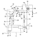
本実施の形態1に係る半導体装置について説明する。図1に示すように、半導体装置1は、導電体2を用いて形成されている。導電体2の上には電力半導体素子としての第1のスイッチング素子3が設けられ、導電体2と電気的に接続されている。導電体2の上で、第1のスイッチング素子3と離間して、裏面高耐圧集積回路4が設けられている。
本実施の形態2に係る半導体装置について説明する。ここでは、実施の形態1と異なる点を中心に説明する。
本実施の形態3に係る半導体装置について説明する。ここでは、実施の形態2と異なる点を中心に説明する。
本実施の形態4に係る半導体装置について説明する。ここでは、実施の形態3と異なる点を中心に説明する。
Claims (3)
- 入力側コイル及び出力側コイルを有し、前記入力側コイルに第1の電圧以上の電圧が印加されると前記出力側コイルに電流が流れる負荷コイルと、
導電体と、
前記導電体上で前記導電体と電気的に接続され、表面と裏面との間の耐圧が第1の耐圧であり、入力端子及び出力端子を有し、前記出力端子が前記負荷コイルの前記入力側コイルの一端に接続され、前記負荷コイルの前記入力側コイルに電圧を印加する第1のスイッチング素子と、
前記導電体上で前記第1のスイッチング素子と離間して設けられ、表面と裏面との耐圧が前記第1の耐圧よりも大きい第2の耐圧である裏面高耐圧集積回路と、
前記導電体上で前記第1のスイッチング素子及び前記裏面高耐圧集積回路と離間して設けられた絶縁基板と、
前記絶縁基板に接続された入出力用の配線と、
前記絶縁基板と前記第1のスイッチング素子とを接続する第1の配線と、
前記絶縁基板と前記裏面高耐圧集積回路とを接続する第2の配線とを有し、
前記裏面高耐圧集積回路は、
前記第1のスイッチング素子の前記入力端子に接続され、前記第1のスイッチング素子のオン・オフを制御する制御回路と、
前記負荷コイルの前記入力側コイルに接続されたコレクタと、接地されたエミッタと、前記負荷コイルの前記入力側コイルの電圧が出力されるベースとを有するサイリスタと、
一方の端子が前記サイリスタの前記ベースに接続され、他方の端子が接地されたツェナーダイオードとを含み、
前記第1のスイッチング素子がオンし、前記ツェナーダイオードの前記一方の端子に出力される電圧が前記第1の電圧よりも高い第2の電圧以上である場合、前記ツェナーダイオードの前記一方の端子から前記ツェナーダイオードの前記他方の端子に電流が流れることを特徴とする半導体装置。 - 前記負荷コイルの前記入力側コイルの他端に接続された外部電源と、
前記負荷コイルの前記入力側コイルを介して前記外部電源に接続された入力端子と、前記サイリスタの前記コレクタに接続された出力端子とを有する第2のスイッチング素子と、
一端が前記制御回路及び前記サイリスタの前記エミッタに接続され、他端が接地されたコンデンサとを更に含み、
前記第1のスイッチング素子がオフした場合に、前記外部電源から供給される電圧により前記第2のスイッチング素子がオンし、前記外部電源から前記サイリスタを介して前記コンデンサに電流が流れて前記コンデンサが充電され、
前記制御回路は、前記充電されたコンデンサを電源として前記第1のスイッチング素子のオン・オフを制御することを特徴とする請求項1に記載の半導体装置。 - 前記コンデンサには、前記制御回路に入力信号を与えるための無線モジュールが接続され、
前記無線モジュールは、前記コンデンサを電源として用いることを特徴とする請求項2に記載の半導体装置。
Priority Applications (5)
| Application Number | Priority Date | Filing Date | Title |
|---|---|---|---|
| JP2006294207A JP4957183B2 (ja) | 2006-10-30 | 2006-10-30 | 裏面高耐圧集積回路を用いた半導体装置 |
| US11/673,756 US7787225B2 (en) | 2006-10-30 | 2007-02-12 | Semiconductor apparatus using back-side high-withstand-voltage integrated circuit |
| KR1020070098591A KR100924742B1 (ko) | 2006-10-30 | 2007-10-01 | 이면 고내압 집적회로를 사용한 반도체 장치 |
| DE102007047727.0A DE102007047727B4 (de) | 2006-10-30 | 2007-10-05 | Halbleitervorrichtung, welche eine integrierte Schaltung mit hoher Rückseiten-Spannungsfestigkeit verwendet |
| CNB2007101622774A CN100550379C (zh) | 2006-10-30 | 2007-10-08 | 使用背面高耐压集成电路的半导体装置 |
Applications Claiming Priority (1)
| Application Number | Priority Date | Filing Date | Title |
|---|---|---|---|
| JP2006294207A JP4957183B2 (ja) | 2006-10-30 | 2006-10-30 | 裏面高耐圧集積回路を用いた半導体装置 |
Publications (2)
| Publication Number | Publication Date |
|---|---|
| JP2008112828A JP2008112828A (ja) | 2008-05-15 |
| JP4957183B2 true JP4957183B2 (ja) | 2012-06-20 |
Family
ID=39265102
Family Applications (1)
| Application Number | Title | Priority Date | Filing Date |
|---|---|---|---|
| JP2006294207A Active JP4957183B2 (ja) | 2006-10-30 | 2006-10-30 | 裏面高耐圧集積回路を用いた半導体装置 |
Country Status (5)
| Country | Link |
|---|---|
| US (1) | US7787225B2 (ja) |
| JP (1) | JP4957183B2 (ja) |
| KR (1) | KR100924742B1 (ja) |
| CN (1) | CN100550379C (ja) |
| DE (1) | DE102007047727B4 (ja) |
Cited By (1)
| Publication number | Priority date | Publication date | Assignee | Title |
|---|---|---|---|---|
| US10651113B2 (en) | 2016-05-31 | 2020-05-12 | Mitsubishi Electric Corporation | Semiconductor apparatus, ignition device for internal combustion engine, and internal combustion engine system |
Families Citing this family (6)
| Publication number | Priority date | Publication date | Assignee | Title |
|---|---|---|---|---|
| JP5157247B2 (ja) * | 2006-10-30 | 2013-03-06 | 三菱電機株式会社 | 電力半導体装置 |
| JP4781400B2 (ja) | 2008-06-20 | 2011-09-28 | 三菱電機株式会社 | 半導体装置 |
| JP5171979B2 (ja) * | 2011-04-08 | 2013-03-27 | 三菱電機株式会社 | 電子制御装置 |
| JP5209090B2 (ja) * | 2011-07-04 | 2013-06-12 | 三菱電機株式会社 | 半導体装置 |
| ITMI20131189A1 (it) * | 2013-07-16 | 2015-01-17 | Eldor Corp Spa | Sistema di accensione elettronica per un motore endotermico |
| JP6275282B2 (ja) * | 2015-01-13 | 2018-02-07 | 三菱電機株式会社 | 半導体装置、その製造方法および半導体モジュール |
Family Cites Families (11)
| Publication number | Priority date | Publication date | Assignee | Title |
|---|---|---|---|---|
| JPH04185282A (ja) * | 1990-11-20 | 1992-07-02 | Sanyo Electric Co Ltd | スイッチング電源用混成集積回路装置 |
| JPH0563139A (ja) * | 1991-09-03 | 1993-03-12 | Fuji Electric Co Ltd | 半導体装置 |
| JP3381617B2 (ja) * | 1998-04-03 | 2003-03-04 | 富士電機株式会社 | スイッチング電源制御用半導体装置およびそれを備えたスイッチング電源 |
| JP3955396B2 (ja) * | 1998-09-17 | 2007-08-08 | 株式会社ルネサステクノロジ | 半導体サージ吸収素子 |
| JP3707942B2 (ja) * | 1998-12-17 | 2005-10-19 | 三菱電機株式会社 | 半導体装置とそれを用いた半導体回路 |
| JP2002116237A (ja) * | 2000-10-10 | 2002-04-19 | Texas Instr Japan Ltd | 半導体集積回路 |
| JP2002217416A (ja) * | 2001-01-16 | 2002-08-02 | Hitachi Ltd | 半導体装置 |
| US6649978B2 (en) * | 2001-06-19 | 2003-11-18 | Koninklijke Philips Electronics N.V. | Semiconductor module having multiple semiconductor chips |
| JP4489485B2 (ja) * | 2004-03-31 | 2010-06-23 | 株式会社ルネサステクノロジ | 半導体装置 |
| JP4565879B2 (ja) * | 2004-04-19 | 2010-10-20 | ルネサスエレクトロニクス株式会社 | 半導体装置 |
| JP2006203470A (ja) | 2005-01-19 | 2006-08-03 | Kyocera Corp | 高周波モジュール及び無線通信機器 |
-
2006
- 2006-10-30 JP JP2006294207A patent/JP4957183B2/ja active Active
-
2007
- 2007-02-12 US US11/673,756 patent/US7787225B2/en active Active
- 2007-10-01 KR KR1020070098591A patent/KR100924742B1/ko active Active
- 2007-10-05 DE DE102007047727.0A patent/DE102007047727B4/de active Active
- 2007-10-08 CN CNB2007101622774A patent/CN100550379C/zh active Active
Cited By (2)
| Publication number | Priority date | Publication date | Assignee | Title |
|---|---|---|---|---|
| US10651113B2 (en) | 2016-05-31 | 2020-05-12 | Mitsubishi Electric Corporation | Semiconductor apparatus, ignition device for internal combustion engine, and internal combustion engine system |
| DE112016006919B4 (de) | 2016-05-31 | 2021-09-16 | Mitsubishi Electric Corporation | Halbleitervorrichtung, Zündeinrichtung für Verbrennungsmotor und Verbrennungsmotorsystem |
Also Published As
| Publication number | Publication date |
|---|---|
| CN100550379C (zh) | 2009-10-14 |
| DE102007047727B4 (de) | 2014-05-28 |
| US7787225B2 (en) | 2010-08-31 |
| KR100924742B1 (ko) | 2009-11-05 |
| US20080099838A1 (en) | 2008-05-01 |
| CN101174618A (zh) | 2008-05-07 |
| KR20080039217A (ko) | 2008-05-07 |
| DE102007047727A1 (de) | 2008-05-08 |
| JP2008112828A (ja) | 2008-05-15 |
Similar Documents
| Publication | Publication Date | Title |
|---|---|---|
| CN100550379C (zh) | 使用背面高耐压集成电路的半导体装置 | |
| CN105991118B (zh) | 点火器用半导体装置、点火器系统及点火线圈单元 | |
| JP2010278188A (ja) | 半導体集積回路装置 | |
| JP2004036438A (ja) | 点火装置等の内燃機関用の電子装置 | |
| JP2009147995A (ja) | 電力供給制御回路 | |
| JP6922563B2 (ja) | 半導体装置 | |
| US5781047A (en) | Ignition coil driver module | |
| JP2014013798A (ja) | ワンチップイグナイタ及び内燃機関点火装置 | |
| JP2014013796A (ja) | ワンチップイグナイタ及び内燃機関点火装置 | |
| JP2012174983A (ja) | 集積回路 | |
| JP4360298B2 (ja) | 内燃機関用点火装置 | |
| JP6707874B2 (ja) | 半導体装置 | |
| JP5095979B2 (ja) | 過電圧保護回路 | |
| US6787881B2 (en) | Integrated power device with improved efficiency and reduced overall dimensions | |
| JP2001244463A (ja) | 半導体装置 | |
| KR20110139886A (ko) | 인버터의 게이트 드라이브 회로 | |
| US8044652B2 (en) | Constant current control circuit | |
| JP2008309146A (ja) | 内燃機関用点火装置 | |
| JP4590387B2 (ja) | グロープラグ駆動装置 | |
| JP2014013797A (ja) | ワンチップイグナイタ及び内燃機関点火装置 | |
| JP2008182109A (ja) | 点火コイル | |
| JP2011074905A (ja) | 内燃機関用の点火イグナイタ | |
| JP2022148509A (ja) | ラッチアップ防止回路、半導体装置、電子機器、車両 | |
| JP2009281235A (ja) | 内燃機関用点火コイルのパワースイッチユニット | |
| JP2008160283A (ja) | 負荷駆動回路およびそれを用いた点火装置 |
Legal Events
| Date | Code | Title | Description |
|---|---|---|---|
| A621 | Written request for application examination |
Free format text: JAPANESE INTERMEDIATE CODE: A621 Effective date: 20090212 |
|
| A977 | Report on retrieval |
Free format text: JAPANESE INTERMEDIATE CODE: A971007 Effective date: 20090428 |
|
| A131 | Notification of reasons for refusal |
Free format text: JAPANESE INTERMEDIATE CODE: A131 Effective date: 20110927 |
|
| A521 | Request for written amendment filed |
Free format text: JAPANESE INTERMEDIATE CODE: A523 Effective date: 20111101 |
|
| A131 | Notification of reasons for refusal |
Free format text: JAPANESE INTERMEDIATE CODE: A131 Effective date: 20111206 |
|
| A521 | Request for written amendment filed |
Free format text: JAPANESE INTERMEDIATE CODE: A523 Effective date: 20120201 |
|
| TRDD | Decision of grant or rejection written | ||
| A01 | Written decision to grant a patent or to grant a registration (utility model) |
Free format text: JAPANESE INTERMEDIATE CODE: A01 Effective date: 20120221 |
|
| A01 | Written decision to grant a patent or to grant a registration (utility model) |
Free format text: JAPANESE INTERMEDIATE CODE: A01 |
|
| A61 | First payment of annual fees (during grant procedure) |
Free format text: JAPANESE INTERMEDIATE CODE: A61 Effective date: 20120305 |
|
| FPAY | Renewal fee payment (event date is renewal date of database) |
Free format text: PAYMENT UNTIL: 20150330 Year of fee payment: 3 |
|
| R150 | Certificate of patent or registration of utility model |
Ref document number: 4957183 Country of ref document: JP Free format text: JAPANESE INTERMEDIATE CODE: R150 Free format text: JAPANESE INTERMEDIATE CODE: R150 |
|
| R250 | Receipt of annual fees |
Free format text: JAPANESE INTERMEDIATE CODE: R250 |
|
| R250 | Receipt of annual fees |
Free format text: JAPANESE INTERMEDIATE CODE: R250 |
|
| R250 | Receipt of annual fees |
Free format text: JAPANESE INTERMEDIATE CODE: R250 |
|
| R250 | Receipt of annual fees |
Free format text: JAPANESE INTERMEDIATE CODE: R250 |
|
| R250 | Receipt of annual fees |
Free format text: JAPANESE INTERMEDIATE CODE: R250 |
|
| R250 | Receipt of annual fees |
Free format text: JAPANESE INTERMEDIATE CODE: R250 |
|
| R250 | Receipt of annual fees |
Free format text: JAPANESE INTERMEDIATE CODE: R250 |
|
| R250 | Receipt of annual fees |
Free format text: JAPANESE INTERMEDIATE CODE: R250 |
|
| R250 | Receipt of annual fees |
Free format text: JAPANESE INTERMEDIATE CODE: R250 |
|
| R250 | Receipt of annual fees |
Free format text: JAPANESE INTERMEDIATE CODE: R250 |
|
| R250 | Receipt of annual fees |
Free format text: JAPANESE INTERMEDIATE CODE: R250 |