JP4961299B2 - 露光装置およびデバイス製造方法 - Google Patents
露光装置およびデバイス製造方法 Download PDFInfo
- Publication number
- JP4961299B2 JP4961299B2 JP2007206531A JP2007206531A JP4961299B2 JP 4961299 B2 JP4961299 B2 JP 4961299B2 JP 2007206531 A JP2007206531 A JP 2007206531A JP 2007206531 A JP2007206531 A JP 2007206531A JP 4961299 B2 JP4961299 B2 JP 4961299B2
- Authority
- JP
- Japan
- Prior art keywords
- wafer
- liquid
- substrate
- auxiliary plate
- exposure apparatus
- Prior art date
- Legal status (The legal status is an assumption and is not a legal conclusion. Google has not performed a legal analysis and makes no representation as to the accuracy of the status listed.)
- Expired - Fee Related
Links
Images


Classifications
-
- G—PHYSICS
- G03—PHOTOGRAPHY; CINEMATOGRAPHY; ANALOGOUS TECHNIQUES USING WAVES OTHER THAN OPTICAL WAVES; ELECTROGRAPHY; HOLOGRAPHY
- G03F—PHOTOMECHANICAL PRODUCTION OF TEXTURED OR PATTERNED SURFACES, e.g. FOR PRINTING, FOR PROCESSING OF SEMICONDUCTOR DEVICES; MATERIALS THEREFOR; ORIGINALS THEREFOR; APPARATUS SPECIALLY ADAPTED THEREFOR
- G03F7/00—Photomechanical, e.g. photolithographic, production of textured or patterned surfaces, e.g. printing surfaces; Materials therefor, e.g. comprising photoresists; Apparatus specially adapted therefor
- G03F7/70—Microphotolithographic exposure; Apparatus therefor
- G03F7/70216—Mask projection systems
- G03F7/70341—Details of immersion lithography aspects, e.g. exposure media or control of immersion liquid supply
-
- G—PHYSICS
- G03—PHOTOGRAPHY; CINEMATOGRAPHY; ANALOGOUS TECHNIQUES USING WAVES OTHER THAN OPTICAL WAVES; ELECTROGRAPHY; HOLOGRAPHY
- G03F—PHOTOMECHANICAL PRODUCTION OF TEXTURED OR PATTERNED SURFACES, e.g. FOR PRINTING, FOR PROCESSING OF SEMICONDUCTOR DEVICES; MATERIALS THEREFOR; ORIGINALS THEREFOR; APPARATUS SPECIALLY ADAPTED THEREFOR
- G03F7/00—Photomechanical, e.g. photolithographic, production of textured or patterned surfaces, e.g. printing surfaces; Materials therefor, e.g. comprising photoresists; Apparatus specially adapted therefor
- G03F7/70—Microphotolithographic exposure; Apparatus therefor
- G03F7/70691—Handling of masks or workpieces
- G03F7/707—Chucks, e.g. chucking or un-chucking operations or structural details
-
- G—PHYSICS
- G03—PHOTOGRAPHY; CINEMATOGRAPHY; ANALOGOUS TECHNIQUES USING WAVES OTHER THAN OPTICAL WAVES; ELECTROGRAPHY; HOLOGRAPHY
- G03F—PHOTOMECHANICAL PRODUCTION OF TEXTURED OR PATTERNED SURFACES, e.g. FOR PRINTING, FOR PROCESSING OF SEMICONDUCTOR DEVICES; MATERIALS THEREFOR; ORIGINALS THEREFOR; APPARATUS SPECIALLY ADAPTED THEREFOR
- G03F7/00—Photomechanical, e.g. photolithographic, production of textured or patterned surfaces, e.g. printing surfaces; Materials therefor, e.g. comprising photoresists; Apparatus specially adapted therefor
- G03F7/70—Microphotolithographic exposure; Apparatus therefor
- G03F7/70691—Handling of masks or workpieces
- G03F7/70716—Stages
-
- H—ELECTRICITY
- H10—SEMICONDUCTOR DEVICES; ELECTRIC SOLID-STATE DEVICES NOT OTHERWISE PROVIDED FOR
- H10P—GENERIC PROCESSES OR APPARATUS FOR THE MANUFACTURE OR TREATMENT OF DEVICES COVERED BY CLASS H10
- H10P72/00—Handling or holding of wafers, substrates or devices during manufacture or treatment thereof
- H10P72/70—Handling or holding of wafers, substrates or devices during manufacture or treatment thereof for supporting or gripping
Landscapes
- Physics & Mathematics (AREA)
- General Physics & Mathematics (AREA)
- Exposure Of Semiconductors, Excluding Electron Or Ion Beam Exposure (AREA)
- Exposure And Positioning Against Photoresist Photosensitive Materials (AREA)
- Container, Conveyance, Adherence, Positioning, Of Wafer (AREA)
Description
前記基板を保持する基板ステージを備え、
前記基板ステージは、
天板と、
前記天板上に設けられていて前記基板を保持する基板保持部と、
前記天板上に前記基板保持部とは別個に設けられていて前記基板保持部に保持された基板の外周を囲むように補助板を保持する補助板保持部と、
を有し、
前記基板保持部は、前記補助板保持部に保持された補助板の裏面と対向する表面を持つ延伸部を有し、
前記補助板の裏面と前記延伸部の表面との間の隙間は、前記基板と前記補助板との間の隙間より狭く、
前記補助板保持部には、前記補助板の裏面と前記延伸部の表面との間の隙間に浸入した液体を回収する回収口が設けられている、
ことを特徴とする露光装置である。
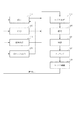
図4は、本実施形態の露光装置1の構成を示す概略断面図である。
このとき、延伸部400aは、表面400cよりも低いのでウエハ40に接触することがない。例えば、ウエハ40を外部の搬送装置から表面400cに搬送する場合、搬送誤差、あるいは、ウエハ40の加工交差によりウエハ40の一部が表面400cから延伸部400aの位置まで飛び出す恐れがある。このとき、本実施形態においては、ウエハ40は延伸部400aと接触することがないので、表面400cに精度良く保持される。
以下、図2を参照して、本発明の別の実施形態の露光装置について説明する。ここで、図2は、本実施形態の露光装置のウエハ40の周辺部の概略断面図である。
以下、図3を参照して、本発明の別の実施形態ついて説明する。ここで、図3は、本実施形態の露光装置のウエハ40の周辺部の概略断面図である。
次に、図7及び図8を参照して、前述の露光装置を利用したデバイス製造方法の実施例を説明する。図7は、デバイスの製造を説明するためのフローチャートである。ここでは、半導体デバイスの製造を例に説明する。ステップ1(回路設計)では、デバイスの回路設計を行う。ステップ2(レチクル製作)では、設計した回路パターンを形成したレチクルを製作する。ステップ3(ウエハ製造)では、シリコンなどの材料を用いてウエハを製造する。ステップ4(ウエハプロセス)は、前工程と呼ばれ、レチクルとウエハを用いてリソグラフィー技術によってウエハ上に実際の回路を形成する。ステップ5(組み立て)は、後工程と呼ばれ、ステップ4によって作成されたウエハを用いて半導体チップ化する工程であり、アッセンブリ工程(ダイシング、ボンディング)、パッケージング工程(チップ封入)等の工程を含む。ステップ6(検査)では、ステップ5で作成された半導体デバイスの動作確認テスト、耐久性テストなどの検査を行う。こうした工程を経て半導体デバイスが完成し、これが出荷(ステップ7)される。
40 ウエハ(基板)
41 ウエハステージ(基板ステージ)
43 補助板
303 天板
400 ウエハ保持部(基板保持部)
400a 延伸部
401 補助板保持部
403 回収口
Claims (5)
- 液体を介して基板を露光する露光装置において、
前記基板を保持する基板ステージを備え、
前記基板ステージは、
天板と、
前記天板上に設けられていて前記基板を保持する基板保持部と、
前記天板上に前記基板保持部とは別個に設けられていて前記基板保持部に保持された基板の外周を囲むように補助板を保持する補助板保持部と、
を有し、
前記基板保持部は、前記補助板保持部に保持された補助板の裏面と対向する表面を持つ延伸部を有し、
前記補助板の裏面と前記延伸部の表面との間の隙間は、前記基板と前記補助板との間の隙間より狭く、
前記補助板保持部には、前記補助板の裏面と前記延伸部の表面との間の隙間に浸入した液体を回収する回収口が設けられている、
ことを特徴とする露光装置。 - 前記延伸部には、前記基板と前記補助板との間の隙間に浸入した液体を回収する回収口が設けられ、
前記延伸部に設けられた回収口を介して液体を吸引する吸引手段を更に備え、
前記基板に対する非露光時には、前記基板と前記補助板との間の隙間に浸入した液体を前記延伸部に設けられた回収口から前記吸引手段により回収し、
前記基板に対する露光時には、前記基板と前記補助板との間の隙間に浸入した液体を前記延伸部に設けられた回収口から重力作用により回収する、
ことを特徴とする請求項1に記載の露光装置。 - 前記補助板の裏面と対向する前記延伸部の表面は、前記基板保持部の前記基板を保持する表面よりも低い、
ことを特徴とする請求項1または請求項2に記載の露光装置。 - 前記延伸部と対向する前記補助板の部分は、前記基板よりも厚い、
ことを特徴とする請求項3に記載の露光装置。 - 請求項1乃至請求項4のいずれか一項に記載の露光装置を用いて基板を露光し、
その露光された基板を現像する、
ことを特徴とするデバイス製造方法。
Priority Applications (4)
| Application Number | Priority Date | Filing Date | Title |
|---|---|---|---|
| JP2007206531A JP4961299B2 (ja) | 2007-08-08 | 2007-08-08 | 露光装置およびデバイス製造方法 |
| TW097129417A TW200923590A (en) | 2007-08-08 | 2008-08-01 | Exposure apparatus and device manufacturing method |
| KR1020080076311A KR20090015824A (ko) | 2007-08-08 | 2008-08-05 | 노광장치 및 디바이스 제조 방법 |
| US12/188,168 US7630056B2 (en) | 2007-08-08 | 2008-08-07 | Exposure apparatus and device manufacturing method |
Applications Claiming Priority (1)
| Application Number | Priority Date | Filing Date | Title |
|---|---|---|---|
| JP2007206531A JP4961299B2 (ja) | 2007-08-08 | 2007-08-08 | 露光装置およびデバイス製造方法 |
Publications (3)
| Publication Number | Publication Date |
|---|---|
| JP2009043879A JP2009043879A (ja) | 2009-02-26 |
| JP2009043879A5 JP2009043879A5 (ja) | 2010-09-16 |
| JP4961299B2 true JP4961299B2 (ja) | 2012-06-27 |
Family
ID=40346177
Family Applications (1)
| Application Number | Title | Priority Date | Filing Date |
|---|---|---|---|
| JP2007206531A Expired - Fee Related JP4961299B2 (ja) | 2007-08-08 | 2007-08-08 | 露光装置およびデバイス製造方法 |
Country Status (4)
| Country | Link |
|---|---|
| US (1) | US7630056B2 (ja) |
| JP (1) | JP4961299B2 (ja) |
| KR (1) | KR20090015824A (ja) |
| TW (1) | TW200923590A (ja) |
Cited By (1)
| Publication number | Priority date | Publication date | Assignee | Title |
|---|---|---|---|---|
| US10018923B2 (en) | 2016-02-17 | 2018-07-10 | Canon Kabushiki Kaisha | Lithography apparatus, and method of manufacturing article |
Families Citing this family (9)
| Publication number | Priority date | Publication date | Assignee | Title |
|---|---|---|---|---|
| JP5001343B2 (ja) | 2008-12-11 | 2012-08-15 | エーエスエムエル ネザーランズ ビー.ブイ. | 流体抽出システム、液浸リソグラフィ装置、及び液浸リソグラフィ装置で使用される液浸液の圧力変動を低減する方法 |
| NL2004305A (en) | 2009-03-13 | 2010-09-14 | Asml Netherlands Bv | Substrate table, immersion lithographic apparatus and device manufacturing method. |
| NL2006127A (en) * | 2010-02-17 | 2011-08-18 | Asml Netherlands Bv | A substrate table, a lithographic apparatus and a method for manufacturing a device using a lithographic apparatus. |
| JP6006406B2 (ja) * | 2012-05-29 | 2016-10-12 | エーエスエムエル ネザーランズ ビー.ブイ. | オブジェクトホルダ及びリソグラフィ装置 |
| EP2856262B1 (en) | 2012-05-29 | 2019-09-25 | ASML Netherlands B.V. | Support apparatus, lithographic apparatus and device manufacturing method |
| WO2016173779A1 (en) | 2015-04-29 | 2016-11-03 | Asml Netherlands B.V. | Support apparatus, lithographic apparatus and device manufacturing method |
| NL2018653A (en) * | 2016-05-12 | 2017-11-15 | Asml Netherlands Bv | Extraction body for lithographic apparatus |
| NL2020011A (en) * | 2017-01-26 | 2018-08-01 | Asml Netherlands Bv | A lithography apparatus and a method of manufacturing a device |
| WO2021170320A1 (en) * | 2020-02-24 | 2021-09-02 | Asml Netherlands B.V. | Substrate support and substrate table |
Family Cites Families (22)
| Publication number | Priority date | Publication date | Assignee | Title |
|---|---|---|---|---|
| SG121819A1 (en) * | 2002-11-12 | 2006-05-26 | Asml Netherlands Bv | Lithographic apparatus and device manufacturing method |
| US7213963B2 (en) * | 2003-06-09 | 2007-05-08 | Asml Netherlands B.V. | Lithographic apparatus and device manufacturing method |
| EP3104396B1 (en) * | 2003-06-13 | 2018-03-21 | Nikon Corporation | Exposure method, substrate stage, exposure apparatus, and device manufacturing method |
| JP3862678B2 (ja) * | 2003-06-27 | 2006-12-27 | キヤノン株式会社 | 露光装置及びデバイス製造方法 |
| JP2005175016A (ja) * | 2003-12-08 | 2005-06-30 | Canon Inc | 基板保持装置およびそれを用いた露光装置ならびにデバイス製造方法 |
| KR101281397B1 (ko) * | 2003-12-15 | 2013-07-02 | 가부시키가이샤 니콘 | 스테이지 장치, 노광 장치, 및 노광 방법 |
| JP4600286B2 (ja) * | 2003-12-16 | 2010-12-15 | 株式会社ニコン | ステージ装置、露光装置、及び露光方法 |
| JP4826146B2 (ja) * | 2004-06-09 | 2011-11-30 | 株式会社ニコン | 露光装置、デバイス製造方法 |
| US7701550B2 (en) * | 2004-08-19 | 2010-04-20 | Asml Netherlands B.V. | Lithographic apparatus and device manufacturing method |
| US8102512B2 (en) * | 2004-09-17 | 2012-01-24 | Nikon Corporation | Substrate holding device, exposure apparatus, and device manufacturing method |
| JP4848956B2 (ja) * | 2004-11-01 | 2011-12-28 | 株式会社ニコン | 露光装置、露光方法、及びデバイス製造方法 |
| WO2006064851A1 (ja) * | 2004-12-15 | 2006-06-22 | Nikon Corporation | 基板保持装置、露光装置、及びデバイス製造方法 |
| JP2006173527A (ja) * | 2004-12-20 | 2006-06-29 | Sony Corp | 露光装置 |
| TWI424260B (zh) * | 2005-03-18 | 2014-01-21 | 尼康股份有限公司 | A board member, a substrate holding device, an exposure apparatus and an exposure method, and a device manufacturing method |
| JP4752320B2 (ja) * | 2005-04-28 | 2011-08-17 | 株式会社ニコン | 基板保持装置及び露光装置、基板保持方法、露光方法、並びにデバイス製造方法 |
| JP2007019392A (ja) * | 2005-07-11 | 2007-01-25 | Canon Inc | 露光装置 |
| JP3997244B2 (ja) | 2005-10-04 | 2007-10-24 | キヤノン株式会社 | 露光装置及びデバイス製造方法 |
| US7420194B2 (en) * | 2005-12-27 | 2008-09-02 | Asml Netherlands B.V. | Lithographic apparatus and substrate edge seal |
| US7839483B2 (en) * | 2005-12-28 | 2010-11-23 | Asml Netherlands B.V. | Lithographic apparatus, device manufacturing method and a control system |
| US8027019B2 (en) * | 2006-03-28 | 2011-09-27 | Asml Netherlands B.V. | Lithographic apparatus and device manufacturing method |
| US9013672B2 (en) * | 2007-05-04 | 2015-04-21 | Asml Netherlands B.V. | Cleaning device, a lithographic apparatus and a lithographic apparatus cleaning method |
| US8514365B2 (en) * | 2007-06-01 | 2013-08-20 | Asml Netherlands B.V. | Lithographic apparatus and device manufacturing method |
-
2007
- 2007-08-08 JP JP2007206531A patent/JP4961299B2/ja not_active Expired - Fee Related
-
2008
- 2008-08-01 TW TW097129417A patent/TW200923590A/zh unknown
- 2008-08-05 KR KR1020080076311A patent/KR20090015824A/ko not_active Ceased
- 2008-08-07 US US12/188,168 patent/US7630056B2/en not_active Expired - Fee Related
Cited By (1)
| Publication number | Priority date | Publication date | Assignee | Title |
|---|---|---|---|---|
| US10018923B2 (en) | 2016-02-17 | 2018-07-10 | Canon Kabushiki Kaisha | Lithography apparatus, and method of manufacturing article |
Also Published As
| Publication number | Publication date |
|---|---|
| US20090040481A1 (en) | 2009-02-12 |
| US7630056B2 (en) | 2009-12-08 |
| JP2009043879A (ja) | 2009-02-26 |
| TW200923590A (en) | 2009-06-01 |
| KR20090015824A (ko) | 2009-02-12 |
Similar Documents
| Publication | Publication Date | Title |
|---|---|---|
| JP4961299B2 (ja) | 露光装置およびデバイス製造方法 | |
| CN101872135B (zh) | 曝光设备和器件制造法 | |
| US20080043211A1 (en) | Apparatus and methods for recovering fluid in immersion lithography | |
| EP1610361B1 (en) | Exposure system and device production method | |
| KR101498439B1 (ko) | 노광 방법 및 노광 장치, 그리고 디바이스 제조 방법 | |
| JP5655921B2 (ja) | メンテナンス方法、露光装置、及びデバイス製造方法 | |
| US8289497B2 (en) | Apparatus and methods for recovering fluid in immersion lithography | |
| KR101647859B1 (ko) | 다수의 다공성 재료들을 이용하여 다공성 재료에서의 진공을 제어하는 장치 및 방법 | |
| US9519229B2 (en) | Apparatus and methods for inhibiting immersion liquid from flowing below a sustrate | |
| TW201306091A (zh) | 基板保持裝置、曝光裝置、以及元件製造方法 | |
| JP2008227452A (ja) | 露光装置およびデバイス製造方法 | |
| US20080106718A1 (en) | Exposure Apparatus and Device Manufacturing Method | |
| JP2007005362A (ja) | 液浸露光装置 | |
| JP2009267235A (ja) | 露光装置 | |
| JP2006261606A (ja) | 露光装置、露光方法及びデバイス製造方法 | |
| JP2007184336A (ja) | 露光装置及びデバイス製造方法 | |
| US8780323B2 (en) | Apparatus and method for recovering liquid droplets in immersion lithography | |
| JP4752320B2 (ja) | 基板保持装置及び露光装置、基板保持方法、露光方法、並びにデバイス製造方法 | |
| WO2006106907A1 (ja) | 露光装置、露光方法及びデバイス製造方法 | |
| JP2009094145A (ja) | 露光装置、露光方法およびデバイス製造方法 | |
| WO2006106851A1 (ja) | 露光装置、露光方法及びデバイス製造方法 | |
| JP2008262963A (ja) | 液浸露光装置およびデバイス製造方法 | |
| US20120257179A1 (en) | Apparatus and methods to recover liquid in immersion lithography | |
| JP2006310827A (ja) | 露光装置、露光方法、及びデバイス製造方法 | |
| JP2007012954A (ja) | 露光装置 |
Legal Events
| Date | Code | Title | Description |
|---|---|---|---|
| RD04 | Notification of resignation of power of attorney |
Free format text: JAPANESE INTERMEDIATE CODE: A7424 Effective date: 20100201 |
|
| RD01 | Notification of change of attorney |
Free format text: JAPANESE INTERMEDIATE CODE: A7421 Effective date: 20100630 |
|
| A521 | Request for written amendment filed |
Free format text: JAPANESE INTERMEDIATE CODE: A523 Effective date: 20100803 |
|
| A621 | Written request for application examination |
Free format text: JAPANESE INTERMEDIATE CODE: A621 Effective date: 20100803 |
|
| A977 | Report on retrieval |
Free format text: JAPANESE INTERMEDIATE CODE: A971007 Effective date: 20120224 |
|
| TRDD | Decision of grant or rejection written | ||
| A01 | Written decision to grant a patent or to grant a registration (utility model) |
Free format text: JAPANESE INTERMEDIATE CODE: A01 Effective date: 20120228 |
|
| A01 | Written decision to grant a patent or to grant a registration (utility model) |
Free format text: JAPANESE INTERMEDIATE CODE: A01 |
|
| A61 | First payment of annual fees (during grant procedure) |
Free format text: JAPANESE INTERMEDIATE CODE: A61 Effective date: 20120326 |
|
| FPAY | Renewal fee payment (event date is renewal date of database) |
Free format text: PAYMENT UNTIL: 20150330 Year of fee payment: 3 |
|
| LAPS | Cancellation because of no payment of annual fees |