JP4970041B2 - 液晶表示装置 - Google Patents
液晶表示装置 Download PDFInfo
- Publication number
- JP4970041B2 JP4970041B2 JP2006539288A JP2006539288A JP4970041B2 JP 4970041 B2 JP4970041 B2 JP 4970041B2 JP 2006539288 A JP2006539288 A JP 2006539288A JP 2006539288 A JP2006539288 A JP 2006539288A JP 4970041 B2 JP4970041 B2 JP 4970041B2
- Authority
- JP
- Japan
- Prior art keywords
- electrode
- liquid crystal
- sub
- subpixel
- auxiliary capacitance
- Prior art date
- Legal status (The legal status is an assumption and is not a legal conclusion. Google has not performed a legal analysis and makes no representation as to the accuracy of the status listed.)
- Expired - Lifetime
Links
Images


Classifications
-
- G—PHYSICS
- G02—OPTICS
- G02F—OPTICAL DEVICES OR ARRANGEMENTS FOR THE CONTROL OF LIGHT BY MODIFICATION OF THE OPTICAL PROPERTIES OF THE MEDIA OF THE ELEMENTS INVOLVED THEREIN; NON-LINEAR OPTICS; FREQUENCY-CHANGING OF LIGHT; OPTICAL LOGIC ELEMENTS; OPTICAL ANALOGUE/DIGITAL CONVERTERS
- G02F1/00—Devices or arrangements for the control of the intensity, colour, phase, polarisation or direction of light arriving from an independent light source, e.g. switching, gating or modulating; Non-linear optics
- G02F1/01—Devices or arrangements for the control of the intensity, colour, phase, polarisation or direction of light arriving from an independent light source, e.g. switching, gating or modulating; Non-linear optics for the control of the intensity, phase, polarisation or colour
- G02F1/13—Devices or arrangements for the control of the intensity, colour, phase, polarisation or direction of light arriving from an independent light source, e.g. switching, gating or modulating; Non-linear optics for the control of the intensity, phase, polarisation or colour based on liquid crystals, e.g. single liquid crystal display cells
- G02F1/133—Constructional arrangements; Operation of liquid crystal cells; Circuit arrangements
- G02F1/136—Liquid crystal cells structurally associated with a semi-conducting layer or substrate, e.g. cells forming part of an integrated circuit
- G02F1/1362—Active matrix addressed cells
- G02F1/13624—Active matrix addressed cells having more than one switching element per pixel
-
- G—PHYSICS
- G02—OPTICS
- G02F—OPTICAL DEVICES OR ARRANGEMENTS FOR THE CONTROL OF LIGHT BY MODIFICATION OF THE OPTICAL PROPERTIES OF THE MEDIA OF THE ELEMENTS INVOLVED THEREIN; NON-LINEAR OPTICS; FREQUENCY-CHANGING OF LIGHT; OPTICAL LOGIC ELEMENTS; OPTICAL ANALOGUE/DIGITAL CONVERTERS
- G02F1/00—Devices or arrangements for the control of the intensity, colour, phase, polarisation or direction of light arriving from an independent light source, e.g. switching, gating or modulating; Non-linear optics
- G02F1/01—Devices or arrangements for the control of the intensity, colour, phase, polarisation or direction of light arriving from an independent light source, e.g. switching, gating or modulating; Non-linear optics for the control of the intensity, phase, polarisation or colour
- G02F1/13—Devices or arrangements for the control of the intensity, colour, phase, polarisation or direction of light arriving from an independent light source, e.g. switching, gating or modulating; Non-linear optics for the control of the intensity, phase, polarisation or colour based on liquid crystals, e.g. single liquid crystal display cells
- G02F1/133—Constructional arrangements; Operation of liquid crystal cells; Circuit arrangements
- G02F1/1333—Constructional arrangements; Manufacturing methods
- G02F1/1343—Electrodes
- G02F1/134309—Electrodes characterised by their geometrical arrangement
- G02F1/134336—Matrix
-
- G—PHYSICS
- G02—OPTICS
- G02F—OPTICAL DEVICES OR ARRANGEMENTS FOR THE CONTROL OF LIGHT BY MODIFICATION OF THE OPTICAL PROPERTIES OF THE MEDIA OF THE ELEMENTS INVOLVED THEREIN; NON-LINEAR OPTICS; FREQUENCY-CHANGING OF LIGHT; OPTICAL LOGIC ELEMENTS; OPTICAL ANALOGUE/DIGITAL CONVERTERS
- G02F1/00—Devices or arrangements for the control of the intensity, colour, phase, polarisation or direction of light arriving from an independent light source, e.g. switching, gating or modulating; Non-linear optics
- G02F1/01—Devices or arrangements for the control of the intensity, colour, phase, polarisation or direction of light arriving from an independent light source, e.g. switching, gating or modulating; Non-linear optics for the control of the intensity, phase, polarisation or colour
- G02F1/13—Devices or arrangements for the control of the intensity, colour, phase, polarisation or direction of light arriving from an independent light source, e.g. switching, gating or modulating; Non-linear optics for the control of the intensity, phase, polarisation or colour based on liquid crystals, e.g. single liquid crystal display cells
- G02F1/133—Constructional arrangements; Operation of liquid crystal cells; Circuit arrangements
- G02F1/136—Liquid crystal cells structurally associated with a semi-conducting layer or substrate, e.g. cells forming part of an integrated circuit
- G02F1/1362—Active matrix addressed cells
- G02F1/136213—Storage capacitors associated with the pixel electrode
-
- G—PHYSICS
- G09—EDUCATION; CRYPTOGRAPHY; DISPLAY; ADVERTISING; SEALS
- G09G—ARRANGEMENTS OR CIRCUITS FOR CONTROL OF INDICATING DEVICES USING STATIC MEANS TO PRESENT VARIABLE INFORMATION
- G09G3/00—Control arrangements or circuits, of interest only in connection with visual indicators other than cathode-ray tubes
- G09G3/20—Control arrangements or circuits, of interest only in connection with visual indicators other than cathode-ray tubes for presentation of an assembly of a number of characters, e.g. a page, by composing the assembly by combination of individual elements arranged in a matrix no fixed position being assigned to or needed to be assigned to the individual characters or partial characters
- G09G3/34—Control arrangements or circuits, of interest only in connection with visual indicators other than cathode-ray tubes for presentation of an assembly of a number of characters, e.g. a page, by composing the assembly by combination of individual elements arranged in a matrix no fixed position being assigned to or needed to be assigned to the individual characters or partial characters by control of light from an independent source
- G09G3/36—Control arrangements or circuits, of interest only in connection with visual indicators other than cathode-ray tubes for presentation of an assembly of a number of characters, e.g. a page, by composing the assembly by combination of individual elements arranged in a matrix no fixed position being assigned to or needed to be assigned to the individual characters or partial characters by control of light from an independent source using liquid crystals
- G09G3/3611—Control of matrices with row and column drivers
- G09G3/3648—Control of matrices with row and column drivers using an active matrix
-
- G—PHYSICS
- G02—OPTICS
- G02F—OPTICAL DEVICES OR ARRANGEMENTS FOR THE CONTROL OF LIGHT BY MODIFICATION OF THE OPTICAL PROPERTIES OF THE MEDIA OF THE ELEMENTS INVOLVED THEREIN; NON-LINEAR OPTICS; FREQUENCY-CHANGING OF LIGHT; OPTICAL LOGIC ELEMENTS; OPTICAL ANALOGUE/DIGITAL CONVERTERS
- G02F1/00—Devices or arrangements for the control of the intensity, colour, phase, polarisation or direction of light arriving from an independent light source, e.g. switching, gating or modulating; Non-linear optics
- G02F1/01—Devices or arrangements for the control of the intensity, colour, phase, polarisation or direction of light arriving from an independent light source, e.g. switching, gating or modulating; Non-linear optics for the control of the intensity, phase, polarisation or colour
- G02F1/13—Devices or arrangements for the control of the intensity, colour, phase, polarisation or direction of light arriving from an independent light source, e.g. switching, gating or modulating; Non-linear optics for the control of the intensity, phase, polarisation or colour based on liquid crystals, e.g. single liquid crystal display cells
- G02F1/133—Constructional arrangements; Operation of liquid crystal cells; Circuit arrangements
- G02F1/1333—Constructional arrangements; Manufacturing methods
- G02F1/1343—Electrodes
- G02F1/134309—Electrodes characterised by their geometrical arrangement
- G02F1/134345—Subdivided pixels, e.g. for grey scale or redundancy
-
- G—PHYSICS
- G09—EDUCATION; CRYPTOGRAPHY; DISPLAY; ADVERTISING; SEALS
- G09G—ARRANGEMENTS OR CIRCUITS FOR CONTROL OF INDICATING DEVICES USING STATIC MEANS TO PRESENT VARIABLE INFORMATION
- G09G2300/00—Aspects of the constitution of display devices
- G09G2300/04—Structural and physical details of display devices
- G09G2300/0439—Pixel structures
- G09G2300/0443—Pixel structures with several sub-pixels for the same colour in a pixel, not specifically used to display gradations
- G09G2300/0447—Pixel structures with several sub-pixels for the same colour in a pixel, not specifically used to display gradations for multi-domain technique to improve the viewing angle in a liquid crystal display, such as multi-vertical alignment [MVA]
-
- G—PHYSICS
- G09—EDUCATION; CRYPTOGRAPHY; DISPLAY; ADVERTISING; SEALS
- G09G—ARRANGEMENTS OR CIRCUITS FOR CONTROL OF INDICATING DEVICES USING STATIC MEANS TO PRESENT VARIABLE INFORMATION
- G09G2300/00—Aspects of the constitution of display devices
- G09G2300/08—Active matrix structure, i.e. with use of active elements, inclusive of non-linear two terminal elements, in the pixels together with light emitting or modulating elements
- G09G2300/0876—Supplementary capacities in pixels having special driving circuits and electrodes instead of being connected to common electrode or ground; Use of additional capacitively coupled compensation electrodes
-
- G—PHYSICS
- G09—EDUCATION; CRYPTOGRAPHY; DISPLAY; ADVERTISING; SEALS
- G09G—ARRANGEMENTS OR CIRCUITS FOR CONTROL OF INDICATING DEVICES USING STATIC MEANS TO PRESENT VARIABLE INFORMATION
- G09G2320/00—Control of display operating conditions
- G09G2320/02—Improving the quality of display appearance
- G09G2320/0271—Adjustment of the gradation levels within the range of the gradation scale, e.g. by redistribution or clipping
- G09G2320/0276—Adjustment of the gradation levels within the range of the gradation scale, e.g. by redistribution or clipping for the purpose of adaptation to the characteristics of a display device, i.e. gamma correction
Landscapes
- Physics & Mathematics (AREA)
- Nonlinear Science (AREA)
- Chemical & Material Sciences (AREA)
- Crystallography & Structural Chemistry (AREA)
- General Physics & Mathematics (AREA)
- Engineering & Computer Science (AREA)
- Mathematical Physics (AREA)
- Optics & Photonics (AREA)
- Microelectronics & Electronic Packaging (AREA)
- Computer Hardware Design (AREA)
- Power Engineering (AREA)
- Theoretical Computer Science (AREA)
- Geometry (AREA)
- Liquid Crystal (AREA)
- Liquid Crystal Display Device Control (AREA)
- Control Of Indicators Other Than Cathode Ray Tubes (AREA)
- Devices For Indicating Variable Information By Combining Individual Elements (AREA)
Description
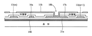
11a,11b,11c,11d 副画素電極
12 走査線
13 信号線
14O,14E 補助容量配線
15a,15b,15c TFT(スイッチング素子)
16a,16b,16c,16d,16e,16a’,16b’ ドレイン電極の延長部
17a,17b 補助容量電極
18a,18b,18c コンタクトホール
19 金属層
21 対向電極
141,142,141’,142’ 補助容量対向電極
SC 半導体層
ClcO,ClcE1,ClcE2 液晶容量
CcsO,CcsE 補助容量
VlcO=Vs−ΔVd+VcsOp(CcsO/CpixO)−Vcom、
VlcE=Vs−ΔVd−VcsEp(CcsE/CpixE)−Vcom
となる。
VlcO=Vs−ΔVd−Vcom
VlcE=Vs−ΔVd−Vcom
VlcOrms=Vs−ΔVd+(1/2)VcsOp(CcsO/CpixO)−Vcom
VlcErms=Vs−ΔVd−(1/2)VcsEp(CcsE/CpixE)−Vcom
(ただし、(Vs−ΔVd−Vcom)>>VcsOp(CcsO/CpixO)、
(Vs−ΔVd−Vcom)>>VcsEp(CcsE/CpixE)時。)
となる。したがって、これら実効値の差をΔVlc=VlcOrms−VlcErmsとすると、
ΔVlc={VcsOp(CcsO/CpixO)+VcsEp(CcsE/CpixE)}/2
となる。このように副画素電極11a〜11cに接続されている補助容量CcsO,CcsEの補助容量対向電極141,142に印加する電圧を制御することによって、副画素電極11a及び副画素電極11b,11cに互いに異なる電圧を印加することができるようになる。
Claims (12)
- 行方向に延びる複数の走査線と、列方向に延びる複数の信号線と、複数の画素を備え、
前記複数の画素のそれぞれが、信号線に沿って列方向に配列された3つの副画素を有し、明副画素が中央に位置し、暗副画素が両側に位置し、
前記明副画素は中間調表示状態において前記暗副画素より高い輝度を呈し、
前記明副画素は明副画素電極を有し、前記暗副画素は暗副画素電極を有し、
前記暗副画素電極とトランジスタのドレイン電極とを接続する接続配線を備え、
隣接する走査線の間には、2本の補助容量配線が走査線と平行に設けられ、
前記接続配線は前記2本の補助容量配線と重なっている液晶表示装置。 - 前記接続配線は前記2本の補助容量配線のうちトランジスタに近い方の補助容量配線と重なる領域で幅広になっている請求項1記載の液晶表示装置。
- 前記2本の補助容量配線は、前記接続配線の幅広部が重なる領域で幅広になっている請求項2記載の液晶表示装置。
- 前記接続配線の幅広になっている上にはコンタクトホールが形成されており、前記接続配線の幅広部が補助容量電極である請求項1乃至3のいずれかに記載の液晶表示装置。
- 前記補助容量配線が幅広になっている箇所が補助容量対向電極であることを特徴とする請求項1乃至4のいずれかに記載の液晶表示装置。
- 前記2本の補助容量配線は、副画素の間に設けられている請求項1乃至5のいずれかに記載の液晶表示装置。
- 前記3つの副画素は、副画素電極と、前記液晶層を介して前記副画素電極と対向する対向電極によって形成された液晶容量と、
前記副画素電極に電気的に接続された前記補助容量電極と、前記補助容量電極と対向し、前記補助容量配線と接続する補助容量対向電極とによって形成された前記補助容量とを有し、
前記対向電極は、3つの副画素に対して共通の単一の電極であり、
前記補助容量配線は、中央に位置する副画素と両側に位置する副画素とで異なる請求項1乃至6のいずれかに記載の液晶表示装置。 - 行方向に延びる走査線と、列方向に延びる信号線と、前記複数の画素のそれぞれの、中央に位置する副画素と両側に位置する副画素のそれぞれに対応して設けられ、それぞれが当該画素に対応する共通の走査線および共通の信号線に接続された少なくとも2つのスイッチング素子とを有し、
前記スイッチング素子は、前記共通の走査線に供給される走査信号電圧によってオン/オフ制御され、前記スイッチング素子がオン状態にあるときに、中央に位置する副画素および両側に位置する副画素のそれぞれが有する前記副画素電極および前記補助容量電極に、共通の信号線から表示信号電圧が供給され、
前記スイッチング素子がオフ状態とされた後に、中央に位置する副画素および両側に位置する副画素のそれぞれの前記補助容量対向電極の電圧が変化し、
その変化の方向および変化の大きさによって規定される変化量が、中央に位置する副画素および両側に位置する副画素とで異なる請求項7に記載の液晶表示装置。 - 前記補助容量対向電圧は所定の周期ごとに極性が反転する請求項8に記載の液晶表示装置。
- 前記中央に位置する副画素の前記補助容量対向電極に印加される補助容量対向電圧と、前記両側に位置する副画素の前記補助容量対向電極に印加される補助容量対向電圧とは、位相が180°異なっている請求項9に記載の液晶表示装置。
- 前記中央に位置する副画素の前記補助容量対向電極に印加される補助容量対向電圧と、前記両側に位置する副画素の前記補助容量対向電極に印加される補助容量対向電圧とは、互いに等しい振幅を有している請求項10に記載の液晶表示装置。
- 前記信号線に印加される表示信号電圧は、互いに隣接する信号線間で極性が逆であり、行方向に隣り合う画素において、中央に位置する副画素および両側に位置する副画素の補助容量電極と対向する補助容量対向電極を逆にした請求項9〜11のいずれかに記載の液晶表示装置。
Priority Applications (1)
| Application Number | Priority Date | Filing Date | Title |
|---|---|---|---|
| JP2006539288A JP4970041B2 (ja) | 2004-10-06 | 2005-10-04 | 液晶表示装置 |
Applications Claiming Priority (4)
| Application Number | Priority Date | Filing Date | Title |
|---|---|---|---|
| JP2004293218 | 2004-10-06 | ||
| JP2004293218 | 2004-10-06 | ||
| JP2006539288A JP4970041B2 (ja) | 2004-10-06 | 2005-10-04 | 液晶表示装置 |
| PCT/JP2005/018313 WO2006038598A1 (ja) | 2004-10-06 | 2005-10-04 | 液晶表示装置 |
Publications (2)
| Publication Number | Publication Date |
|---|---|
| JPWO2006038598A1 JPWO2006038598A1 (ja) | 2008-05-15 |
| JP4970041B2 true JP4970041B2 (ja) | 2012-07-04 |
Family
ID=36142671
Family Applications (1)
| Application Number | Title | Priority Date | Filing Date |
|---|---|---|---|
| JP2006539288A Expired - Lifetime JP4970041B2 (ja) | 2004-10-06 | 2005-10-04 | 液晶表示装置 |
Country Status (6)
| Country | Link |
|---|---|
| US (2) | US8614658B2 (ja) |
| EP (3) | EP1978398B1 (ja) |
| JP (1) | JP4970041B2 (ja) |
| KR (2) | KR100902705B1 (ja) |
| CN (4) | CN101587274B (ja) |
| WO (1) | WO2006038598A1 (ja) |
Families Citing this family (56)
| Publication number | Priority date | Publication date | Assignee | Title |
|---|---|---|---|---|
| JP4658622B2 (ja) * | 2005-01-19 | 2011-03-23 | シャープ株式会社 | 液晶表示装置用基板及び液晶表示装置 |
| TWI405013B (zh) | 2005-06-09 | 2013-08-11 | Sharp Kk | 液晶顯示裝置 |
| US20090009449A1 (en) * | 2006-02-06 | 2009-01-08 | Toshihisa Uchida | Display device, active matrix substrate, liquid crystald display device and television receiver |
| CN101416105B (zh) | 2006-04-04 | 2011-04-13 | 夏普株式会社 | 液晶显示装置 |
| JP5036354B2 (ja) * | 2006-04-04 | 2012-09-26 | 東京エレクトロン株式会社 | 成膜装置の排気系構造、成膜装置、および排ガスの処理方法 |
| EP2363744B1 (en) * | 2006-04-24 | 2015-12-16 | Sharp Kk | Liquid crystal display device |
| EP1860490A1 (en) * | 2006-05-26 | 2007-11-28 | Au Optronics Corporation | Vertical alignment type liquid crystal displays |
| JP5247008B2 (ja) * | 2006-06-07 | 2013-07-24 | キヤノン株式会社 | 透過型の表示装置 |
| CN100533538C (zh) * | 2006-06-09 | 2009-08-26 | 瀚宇彩晶股份有限公司 | 液晶显示器像素结构及其驱动方法 |
| CN100468140C (zh) * | 2006-06-20 | 2009-03-11 | 友达光电股份有限公司 | 垂直配向型液晶显示装置及其像素单元电路 |
| EP2051133B1 (en) * | 2006-07-14 | 2012-11-14 | Sharp Kabushiki Kaisha | Liquid crystal display device |
| CN101501561B (zh) * | 2006-08-10 | 2011-04-06 | 夏普株式会社 | 液晶显示装置 |
| TWI326788B (en) * | 2006-09-29 | 2010-07-01 | Au Optronics Corp | Pixel structure |
| KR101211087B1 (ko) * | 2006-11-30 | 2012-12-12 | 삼성디스플레이 주식회사 | 박막 트랜지스터 기판 및 이를 포함하는 표시 장치 |
| WO2008069181A1 (ja) | 2006-12-05 | 2008-06-12 | Sharp Kabushiki Kaisha | 液晶表示装置 |
| WO2008111490A1 (ja) * | 2007-03-15 | 2008-09-18 | Sharp Kabushiki Kaisha | 液晶表示装置 |
| US9196206B2 (en) * | 2007-04-26 | 2015-11-24 | Sharp Kabushiki Kaisha | Liquid crystal display |
| JP5542296B2 (ja) | 2007-05-17 | 2014-07-09 | 株式会社半導体エネルギー研究所 | 液晶表示装置、表示モジュール及び電子機器 |
| JP5116359B2 (ja) | 2007-05-17 | 2013-01-09 | 株式会社半導体エネルギー研究所 | 液晶表示装置 |
| JP4989309B2 (ja) | 2007-05-18 | 2012-08-01 | 株式会社半導体エネルギー研究所 | 液晶表示装置 |
| WO2008146512A1 (ja) | 2007-05-30 | 2008-12-04 | Sharp Kabushiki Kaisha | アクティブマトリクス基板、液晶パネル、液晶表示ユニット、液晶表示装置およびテレビジョン受像機 |
| JP2009075563A (ja) * | 2007-08-24 | 2009-04-09 | Canon Inc | 発光表示装置の表示方法 |
| TWI373676B (en) * | 2007-09-06 | 2012-10-01 | Au Optronics Corp | Pixel structure and forming method and driving method thereof |
| KR101200655B1 (ko) * | 2007-09-28 | 2012-11-12 | 파나소닉 주식회사 | 발광 소자 회로 및 액티브 매트릭스형 표시 장치 |
| JP5251068B2 (ja) * | 2007-10-17 | 2013-07-31 | 株式会社リコー | アクティブマトリクス基板及び電子表示装置 |
| CN101878448B (zh) * | 2007-11-30 | 2014-01-01 | 夏普株式会社 | 液晶显示装置、有源矩阵基板、液晶面板、液晶显示单元、电视接收机 |
| KR20090060756A (ko) | 2007-12-10 | 2009-06-15 | 삼성전자주식회사 | 표시 패널 및 이의 제조방법 |
| KR101427582B1 (ko) | 2007-12-12 | 2014-08-08 | 삼성디스플레이 주식회사 | 표시판 및 이를 포함하는 액정 표시 장치 |
| JP5162232B2 (ja) * | 2007-12-27 | 2013-03-13 | パナソニック液晶ディスプレイ株式会社 | 表示装置 |
| JP4807371B2 (ja) * | 2008-03-27 | 2011-11-02 | ソニー株式会社 | 液晶表示装置 |
| US8432344B2 (en) * | 2008-05-27 | 2013-04-30 | Samsung Display Co., Ltd. | Liquid crystal display |
| KR101541794B1 (ko) * | 2008-12-09 | 2015-08-04 | 삼성디스플레이 주식회사 | 액정 표시 장치 |
| US20120007843A1 (en) * | 2009-03-24 | 2012-01-12 | Sharp Kabushiki Kaisha | Tft substrate and liquid crystal display apparatus using the same |
| US20120127416A1 (en) * | 2009-07-03 | 2012-05-24 | Sharp Kabushiki Kaisha | Liquid crystal display device |
| US8947607B2 (en) * | 2010-12-08 | 2015-02-03 | Sharp Kabushiki Kaisha | Active matrix substrate and display device |
| WO2013024670A1 (ja) * | 2011-08-12 | 2013-02-21 | シャープ株式会社 | 表示素子、及びこれを用いた電気機器 |
| TWI559047B (zh) * | 2012-06-13 | 2016-11-21 | 友達光電股份有限公司 | 畫素陣列基板、液晶顯示器以及液晶顯示器的製造方法 |
| JP5961060B2 (ja) * | 2012-07-18 | 2016-08-02 | 株式会社ジャパンディスプレイ | 液晶表示装置 |
| JP5371159B2 (ja) * | 2012-10-16 | 2013-12-18 | 株式会社半導体エネルギー研究所 | 半導体装置 |
| JP5690894B2 (ja) * | 2013-09-16 | 2015-03-25 | 株式会社半導体エネルギー研究所 | 液晶表示装置 |
| KR102129569B1 (ko) * | 2013-11-26 | 2020-07-03 | 삼성디스플레이 주식회사 | 액정 표시 장치 |
| KR102183088B1 (ko) | 2014-02-10 | 2020-11-26 | 삼성디스플레이 주식회사 | 액정 표시 장치 |
| KR101502357B1 (ko) * | 2014-06-19 | 2015-03-16 | 삼성디스플레이 주식회사 | 표시장치 및 그 구동방법 |
| KR102215478B1 (ko) * | 2014-11-27 | 2021-02-15 | 삼성디스플레이 주식회사 | 표시 장치 및 그 구동 방법 |
| JP5859632B2 (ja) * | 2014-12-22 | 2016-02-10 | 株式会社半導体エネルギー研究所 | 表示装置 |
| CN104536225B (zh) | 2014-12-31 | 2018-09-18 | 深圳市华星光电技术有限公司 | 液晶显示面板及液晶显示装置 |
| KR102561194B1 (ko) * | 2016-07-21 | 2023-07-28 | 삼성디스플레이 주식회사 | 표시 장치 |
| CN106773395B (zh) * | 2016-12-21 | 2019-08-13 | 深圳市华星光电技术有限公司 | 一种液晶显示面板的像素结构及显示装置 |
| JP6379259B2 (ja) * | 2017-06-30 | 2018-08-22 | 株式会社半導体エネルギー研究所 | 表示装置、及び電子機器 |
| KR102367963B1 (ko) * | 2017-07-13 | 2022-02-25 | 삼성디스플레이 주식회사 | 액정 표시 장치 |
| CN108172193B (zh) * | 2018-03-22 | 2021-01-26 | 京东方科技集团股份有限公司 | 一种显示面板、显示装置及其驱动方法 |
| JP6895574B2 (ja) * | 2019-07-25 | 2021-06-30 | 株式会社半導体エネルギー研究所 | 透過型の液晶表示装置 |
| JP2022153393A (ja) * | 2019-12-13 | 2022-10-12 | 株式会社半導体エネルギー研究所 | 液晶表示装置 |
| US11442272B2 (en) * | 2020-03-12 | 2022-09-13 | Facebook Technologies, Llc | High-resolution liquid crystal displays |
| JP7237439B1 (ja) | 2022-07-01 | 2023-03-13 | 株式会社半導体エネルギー研究所 | 透過型液晶表示装置、電子機器 |
| JP2023123683A (ja) * | 2022-07-01 | 2023-09-05 | 株式会社半導体エネルギー研究所 | 液晶表示装置 |
Family Cites Families (20)
| Publication number | Priority date | Publication date | Assignee | Title |
|---|---|---|---|---|
| JPS5691277A (en) | 1979-12-25 | 1981-07-24 | Citizen Watch Co Ltd | Liquiddcrystal display panel |
| FI74871B (fi) | 1986-06-26 | 1987-12-31 | Sinisalo Sport Oy | Skyddsklaede. |
| US5204659A (en) * | 1987-11-13 | 1993-04-20 | Honeywell Inc. | Apparatus and method for providing a gray scale in liquid crystal flat panel displays |
| US5245450A (en) * | 1990-07-23 | 1993-09-14 | Hosiden Corporation | Liquid crystal display device with control capacitors for gray-scale |
| JP3401049B2 (ja) | 1993-05-26 | 2003-04-28 | コーニンクレッカ フィリップス エレクトロニクス エヌ ヴィ | 階調液晶表示パネル |
| JP2004029716A (ja) * | 1995-02-01 | 2004-01-29 | Seiko Epson Corp | 液晶表示装置 |
| JP3312720B2 (ja) * | 1996-11-26 | 2002-08-12 | シャープ株式会社 | 液晶表示装置 |
| TW373114B (en) | 1996-08-05 | 1999-11-01 | Sharp Kk | Liquid crystal display device |
| JP3395877B2 (ja) | 1996-12-20 | 2003-04-14 | シャープ株式会社 | 液晶表示装置及びその製造方法 |
| TW509808B (en) | 1997-06-12 | 2002-11-11 | Sharp Kk | Liquid crystal display device |
| JP3645184B2 (ja) * | 2000-05-31 | 2005-05-11 | シャープ株式会社 | 液晶表示装置及びその欠陥修正方法 |
| JP2002333870A (ja) * | 2000-10-31 | 2002-11-22 | Matsushita Electric Ind Co Ltd | 液晶表示装置、el表示装置及びその駆動方法、並びに副画素の表示パターン評価方法 |
| JP2002151699A (ja) * | 2000-11-15 | 2002-05-24 | Casio Comput Co Ltd | アクティブマトリクス型液晶表示装置 |
| US6956553B2 (en) | 2001-04-27 | 2005-10-18 | Sanyo Electric Co., Ltd. | Active matrix display device |
| JP4342200B2 (ja) | 2002-06-06 | 2009-10-14 | シャープ株式会社 | 液晶表示装置 |
| JP4248306B2 (ja) * | 2002-06-17 | 2009-04-02 | シャープ株式会社 | 液晶表示装置 |
| JP3940385B2 (ja) * | 2002-12-19 | 2007-07-04 | 株式会社神戸製鋼所 | 表示デバイスおよびその製法 |
| KR100643039B1 (ko) * | 2003-12-11 | 2006-11-10 | 엘지.필립스 엘시디 주식회사 | 횡전계형 액정표시장치 |
| JP4108078B2 (ja) | 2004-01-28 | 2008-06-25 | シャープ株式会社 | アクティブマトリクス基板及び表示装置 |
| JP4361844B2 (ja) | 2004-07-28 | 2009-11-11 | 富士通株式会社 | 液晶表示装置 |
-
2005
- 2005-10-04 EP EP08013136A patent/EP1978398B1/en not_active Expired - Lifetime
- 2005-10-04 CN CN2009101505549A patent/CN101587274B/zh not_active Expired - Fee Related
- 2005-10-04 KR KR1020077010345A patent/KR100902705B1/ko not_active Expired - Fee Related
- 2005-10-04 WO PCT/JP2005/018313 patent/WO2006038598A1/ja not_active Ceased
- 2005-10-04 CN CNB2005800341522A patent/CN100523923C/zh not_active Expired - Fee Related
- 2005-10-04 KR KR1020087015761A patent/KR100900115B1/ko not_active Expired - Fee Related
- 2005-10-04 JP JP2006539288A patent/JP4970041B2/ja not_active Expired - Lifetime
- 2005-10-04 EP EP05790494.8A patent/EP1798591B1/en not_active Expired - Lifetime
- 2005-10-04 US US11/663,889 patent/US8614658B2/en not_active Expired - Fee Related
- 2005-10-04 EP EP10167600A patent/EP2230551A3/en not_active Withdrawn
- 2005-10-04 CN CN2008100925505A patent/CN101303495B/zh not_active Expired - Fee Related
- 2005-10-04 CN CN2009101505568A patent/CN101634787B/zh not_active Expired - Fee Related
-
2009
- 2009-03-04 US US12/379,941 patent/US20090195488A1/en not_active Abandoned
Also Published As
| Publication number | Publication date |
|---|---|
| JPWO2006038598A1 (ja) | 2008-05-15 |
| CN100523923C (zh) | 2009-08-05 |
| CN101036080A (zh) | 2007-09-12 |
| KR100900115B1 (ko) | 2009-06-01 |
| EP1798591A1 (en) | 2007-06-20 |
| WO2006038598A1 (ja) | 2006-04-13 |
| KR20070056165A (ko) | 2007-05-31 |
| CN101587274A (zh) | 2009-11-25 |
| EP1798591B1 (en) | 2013-07-24 |
| EP2230551A3 (en) | 2012-05-09 |
| CN101634787B (zh) | 2012-02-29 |
| EP2230551A2 (en) | 2010-09-22 |
| EP1798591A4 (en) | 2009-01-07 |
| US8614658B2 (en) | 2013-12-24 |
| KR100902705B1 (ko) | 2009-06-15 |
| KR20080071203A (ko) | 2008-08-01 |
| CN101303495B (zh) | 2012-01-04 |
| EP1978398A2 (en) | 2008-10-08 |
| US20080122772A1 (en) | 2008-05-29 |
| CN101587274B (zh) | 2012-01-11 |
| EP1978398B1 (en) | 2013-02-13 |
| CN101634787A (zh) | 2010-01-27 |
| US20090195488A1 (en) | 2009-08-06 |
| CN101303495A (zh) | 2008-11-12 |
| EP1978398A3 (en) | 2008-12-31 |
Similar Documents
| Publication | Publication Date | Title |
|---|---|---|
| JP4970041B2 (ja) | 液晶表示装置 | |
| JP4248306B2 (ja) | 液晶表示装置 | |
| JP5259572B2 (ja) | 液晶表示装置 | |
| US7782346B2 (en) | Liquid crystal display | |
| JP5342004B2 (ja) | 液晶表示装置 | |
| JP2011013694A (ja) | 表示装置 | |
| US8441589B2 (en) | Pixel array structure | |
| US9395580B2 (en) | Liquid crystal display | |
| JP5173038B2 (ja) | 液晶表示装置 | |
| JP2017037135A (ja) | 液晶表示装置 | |
| JP5589018B2 (ja) | 液晶表示装置 | |
| KR100920356B1 (ko) | 액정 표시 장치용 박막 다이오드 표시판 및 이를 포함하는액정 표시 장치 |
Legal Events
| Date | Code | Title | Description |
|---|---|---|---|
| A131 | Notification of reasons for refusal |
Free format text: JAPANESE INTERMEDIATE CODE: A131 Effective date: 20100706 |
|
| A521 | Request for written amendment filed |
Free format text: JAPANESE INTERMEDIATE CODE: A523 Effective date: 20100831 |
|
| A131 | Notification of reasons for refusal |
Free format text: JAPANESE INTERMEDIATE CODE: A131 Effective date: 20110705 |
|
| A521 | Request for written amendment filed |
Free format text: JAPANESE INTERMEDIATE CODE: A523 Effective date: 20110905 |
|
| TRDD | Decision of grant or rejection written | ||
| A01 | Written decision to grant a patent or to grant a registration (utility model) |
Free format text: JAPANESE INTERMEDIATE CODE: A01 Effective date: 20120403 |
|
| A01 | Written decision to grant a patent or to grant a registration (utility model) |
Free format text: JAPANESE INTERMEDIATE CODE: A01 |
|
| A61 | First payment of annual fees (during grant procedure) |
Free format text: JAPANESE INTERMEDIATE CODE: A61 Effective date: 20120404 |
|
| FPAY | Renewal fee payment (event date is renewal date of database) |
Free format text: PAYMENT UNTIL: 20150413 Year of fee payment: 3 |
|
| R150 | Certificate of patent or registration of utility model |
Ref document number: 4970041 Country of ref document: JP Free format text: JAPANESE INTERMEDIATE CODE: R150 Free format text: JAPANESE INTERMEDIATE CODE: R150 |
|
| S531 | Written request for registration of change of domicile |
Free format text: JAPANESE INTERMEDIATE CODE: R313531 |
|
| R350 | Written notification of registration of transfer |
Free format text: JAPANESE INTERMEDIATE CODE: R350 |