JP4974563B2 - 光半導体装置 - Google Patents
光半導体装置 Download PDFInfo
- Publication number
- JP4974563B2 JP4974563B2 JP2006095031A JP2006095031A JP4974563B2 JP 4974563 B2 JP4974563 B2 JP 4974563B2 JP 2006095031 A JP2006095031 A JP 2006095031A JP 2006095031 A JP2006095031 A JP 2006095031A JP 4974563 B2 JP4974563 B2 JP 4974563B2
- Authority
- JP
- Japan
- Prior art keywords
- laser chip
- semiconductor laser
- semiconductor device
- light emitting
- emitting element
- Prior art date
- Legal status (The legal status is an assumption and is not a legal conclusion. Google has not performed a legal analysis and makes no representation as to the accuracy of the status listed.)
- Expired - Fee Related
Links
Images




Classifications
-
- H—ELECTRICITY
- H10—SEMICONDUCTOR DEVICES; ELECTRIC SOLID-STATE DEVICES NOT OTHERWISE PROVIDED FOR
- H10W—GENERIC PACKAGES, INTERCONNECTIONS, CONNECTORS OR OTHER CONSTRUCTIONAL DETAILS OF DEVICES COVERED BY CLASS H10
- H10W72/00—Interconnections or connectors in packages
- H10W72/30—Die-attach connectors
Landscapes
- Led Device Packages (AREA)
- Semiconductor Lasers (AREA)
Description
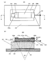
図1から図4は本発明の第1の実施の形態を示す図である。図1に本発明の第1の実施の形態の光半導体装置20の概略構成図を示す。図1(a)は本実施の形態の光半導体装置20の実装状態を上から見た概略構成図、(b)は(a)のA−A線の断面から光半導体装置20の実装状態を見た概略断面図を示す。
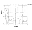
以上のようにハンダ接続層24が固体化すると図1(b)に示すようにハンダ接続層24自体が半導体レーザチップ24のある方向に凸の形状となり、半導体レーザチップ21を含めて全体が室温近辺まで冷えた後もハンダ接続層24の凸の形状は保たれることとなり、半導体レーザチップ21もハンダ接続層24と反対側に凸状に反ると考えられる。
図5に本発明の第2の実施の形態を示す図である。図5に本発明の第2の実施の形態の光半導体装置30の概略構成図を示す。図5(a)は本実施の形態の光半導体装置30の実装状態を上から見た概略構成図、(b)は(a)のB−B線の断面から光半導体装置30の実装状態を見た概略断面図を示す。
図7に本発明の第3の実施の形態の光半導体装置におけるハンダ接続の概略構成図を示す。図7(a)は本実施の形態の光半導体装置のパッケージ上部に相当するキャップ(図示していない)を外して、半導体レーザチップが基台にハンダ接続された状態を示す模式図、(b)は(a)のC−C線の断面から見た半導体レーザチップと基台がハンダ接続された状態の断面図を示す。
2 活性層
3 Si基板
4 表面
5 SiO2膜
6 電極パタン
7,24,34,60 ハンダ接続層
8 メサ部
9 空隙部
10,20,30,41,50 光半導体装置
22,32,46,61 レーザ光
23,33 サブマウント
24a,60a (ハンダ層中の)後端面領域
24b,60b (ハンダ層中の)中央領域
24c,60c (ハンダ層中の)前端面領域
25,35,56 金属基台
26,36 接着面
27a,37a,59a (半導体レーザチップの)後端面部
27b,37b,59b (半導体レーザチップの)中央部
27c,37c,59c (半導体レーザチップの)前端面部
28a,28b,38a,38b,62a,62b 突起部
29a,29b,39a,39b 端面
40a,40b 側面
42 金属ブロック
43 金属製パッケージ
44,44a,44b,44c,57 電極端子
45 導電性ワイヤ
52 受光素子
53 反射ミラー
54 受光素子チップ
55 パッケージ
58 反射点
R1,R2 曲率半径
Θ1,Θ2 角度
ΔB1,ΔB2 反り量
Claims (12)
- 発光素子と、
前記発光素子が接続される基台と、
前記基台と前記発光素子との間に挟まれた接続層とを具備し、
前記発光素子は前記接続層と接する面とは反対側の面上において、前端面部と後端面部とにそれぞれ1つ設けられた一対の突起部を有し、前記基台と反対側に凸状に反っており、
前記接続層は、前記発光素子の前記前端面部と前記後端面部との間の中央部において厚く、前記前端面部および前記後端面部において前記中央部より薄くなっていることを特徴とする光半導体装置。 - 前記発光素子の曲率半径が250mm以上であることを特徴とする請求項1に記載の光半導体装置。
- 前記接続層はハンダ接続層であることを特徴とする請求項1または2に記載の光半導体装置。
- 前記発光素子は略直方体形状で長辺方向に沿って共振器を構成し、前記基台と反対側に凸状の曲率半径で光軸方向に反っていることを特徴とする請求項1から請求項3のいずれか1項に記載の光半導体装置。
- 前記突起部は、前記前端面部及び前記後端面部に沿って帯状に形成されていることを特徴とする請求項1から請求項4のいずれか1項に記載の光半導体装置。
- 前記突起部は、前記発光素子の基板を加工して形成されていることを特徴とする請求項1から請求項5のいずれか1項に記載の光半導体装置。
- 前記突起部は、前記発光素子を構成する材料と同等以上の高さの熱伝導率を有する材料で構成されることを特徴とする請求項1から請求項5のいずれか1項に記載の光半導体装置。
- 前記発光素子は、半導体レーザチップまたは端面発光型発光ダイオードチップであることを特徴とする請求項1から請求項7のいずれか1項に記載の光半導体装置。
- 前記基台は、前記発光素子の活性層に近い表面と対向して前記発光素子と接続されることを特徴とする請求項1から請求項8のいずれか1項に記載の光半導体装置。
- 前記基台はSi基板で構成されていることを特徴とする請求項1から請求項9のいずれか1項に記載の光半導体装置。
- 前記Si基板上に少なくとも受光素子、回路素子または反射ミラーが構成されていることを特徴とする請求項10に記載の光半導体装置。
- 前記基台は、高放熱の金属材料または半導体材料からなることを特徴とする請求項1から請求項11のいずれか1項に記載の光半導体装置。
Priority Applications (3)
| Application Number | Priority Date | Filing Date | Title |
|---|---|---|---|
| JP2006095031A JP4974563B2 (ja) | 2006-03-30 | 2006-03-30 | 光半導体装置 |
| CN200710005407.3A CN101039014B (zh) | 2006-03-15 | 2007-02-08 | 光半导体装置 |
| US11/708,478 US7359416B2 (en) | 2006-03-15 | 2007-02-21 | Optical semiconductor device |
Applications Claiming Priority (1)
| Application Number | Priority Date | Filing Date | Title |
|---|---|---|---|
| JP2006095031A JP4974563B2 (ja) | 2006-03-30 | 2006-03-30 | 光半導体装置 |
Publications (2)
| Publication Number | Publication Date |
|---|---|
| JP2007273574A JP2007273574A (ja) | 2007-10-18 |
| JP4974563B2 true JP4974563B2 (ja) | 2012-07-11 |
Family
ID=38676097
Family Applications (1)
| Application Number | Title | Priority Date | Filing Date |
|---|---|---|---|
| JP2006095031A Expired - Fee Related JP4974563B2 (ja) | 2006-03-15 | 2006-03-30 | 光半導体装置 |
Country Status (1)
| Country | Link |
|---|---|
| JP (1) | JP4974563B2 (ja) |
Families Citing this family (3)
| Publication number | Priority date | Publication date | Assignee | Title |
|---|---|---|---|---|
| JP2012119637A (ja) | 2010-12-03 | 2012-06-21 | Sumitomo Electric Device Innovations Inc | 光半導体装置の製造方法 |
| JP6299494B2 (ja) | 2014-07-09 | 2018-03-28 | 日亜化学工業株式会社 | 発光装置及びその製造方法 |
| JP2015122536A (ja) * | 2015-02-27 | 2015-07-02 | 住友電工デバイス・イノベーション株式会社 | 光半導体装置の製造方法 |
Family Cites Families (3)
| Publication number | Priority date | Publication date | Assignee | Title |
|---|---|---|---|---|
| JP4605850B2 (ja) * | 2000-03-30 | 2011-01-05 | 京セラ株式会社 | 光実装基板の製造方法 |
| JP3889933B2 (ja) * | 2001-03-02 | 2007-03-07 | シャープ株式会社 | 半導体発光装置 |
| JP2003031895A (ja) * | 2001-07-13 | 2003-01-31 | Sharp Corp | 半導体発光装置およびその製造方法 |
-
2006
- 2006-03-30 JP JP2006095031A patent/JP4974563B2/ja not_active Expired - Fee Related
Also Published As
| Publication number | Publication date |
|---|---|
| JP2007273574A (ja) | 2007-10-18 |
Similar Documents
| Publication | Publication Date | Title |
|---|---|---|
| US8275013B2 (en) | Semiconductor laser device and method of manufacturing the same | |
| JP5465514B2 (ja) | 光半導体装置 | |
| US7079563B2 (en) | Semiconductor laser device and method of manufacturing the same | |
| CN101814697A (zh) | 发光装置及其制造方法 | |
| JP2001168442A (ja) | 半導体レーザ素子の製造方法、配設基板および支持基板 | |
| CN101039014B (zh) | 光半导体装置 | |
| US7359416B2 (en) | Optical semiconductor device | |
| US7916766B2 (en) | Semiconductor laser device and manufacturing method thereof | |
| JP5521611B2 (ja) | 光装置および光機器 | |
| JP5959484B2 (ja) | 半導体レーザ素子、及び半導体レーザ装置 | |
| US6895029B2 (en) | Nitride semiconductor laser device | |
| US8138663B2 (en) | Light emitting device and method of manufacturing the same | |
| US20130119118A1 (en) | Method for manufacturing semiconductor laser apparatus, semiconductor laser apparatus, and optical apparatus | |
| CN102195235A (zh) | 发光装置以及采用该发光装置的光学设备 | |
| US7843984B2 (en) | Semiconductor laser device | |
| JP2004319987A (ja) | 半導体レーザ素子 | |
| JP4974563B2 (ja) | 光半導体装置 | |
| JP5227666B2 (ja) | 半導体レーザ装置およびその製造方法 | |
| JP4573882B2 (ja) | 半導体レーザ装置 | |
| JP4917704B2 (ja) | 半導体レーザの製法 | |
| JP2006093466A (ja) | 多波長半導体レーザ素子および多波長半導体レーザ装置 | |
| CN102005700B (zh) | 半导体激光装置 | |
| JP2005259851A (ja) | 半導体レーザ装置 | |
| JP2009200463A (ja) | 半導体装置 | |
| JP2008091768A (ja) | 半導体レーザ装置および電子機器 |
Legal Events
| Date | Code | Title | Description |
|---|---|---|---|
| A621 | Written request for application examination |
Free format text: JAPANESE INTERMEDIATE CODE: A621 Effective date: 20080805 |
|
| A977 | Report on retrieval |
Free format text: JAPANESE INTERMEDIATE CODE: A971007 Effective date: 20101125 |
|
| A131 | Notification of reasons for refusal |
Free format text: JAPANESE INTERMEDIATE CODE: A131 Effective date: 20101221 |
|
| A521 | Request for written amendment filed |
Free format text: JAPANESE INTERMEDIATE CODE: A523 Effective date: 20110218 |
|
| RD02 | Notification of acceptance of power of attorney |
Free format text: JAPANESE INTERMEDIATE CODE: A7422 Effective date: 20120119 |
|
| TRDD | Decision of grant or rejection written | ||
| A01 | Written decision to grant a patent or to grant a registration (utility model) |
Free format text: JAPANESE INTERMEDIATE CODE: A01 Effective date: 20120313 |
|
| A01 | Written decision to grant a patent or to grant a registration (utility model) |
Free format text: JAPANESE INTERMEDIATE CODE: A01 |
|
| A61 | First payment of annual fees (during grant procedure) |
Free format text: JAPANESE INTERMEDIATE CODE: A61 Effective date: 20120410 |
|
| R150 | Certificate of patent or registration of utility model |
Free format text: JAPANESE INTERMEDIATE CODE: R150 |
|
| FPAY | Renewal fee payment (event date is renewal date of database) |
Free format text: PAYMENT UNTIL: 20150420 Year of fee payment: 3 |
|
| LAPS | Cancellation because of no payment of annual fees |