JP4981485B2 - Vapor phase growth method and vapor phase growth apparatus - Google Patents
Vapor phase growth method and vapor phase growth apparatus Download PDFInfo
- Publication number
- JP4981485B2 JP4981485B2 JP2007054424A JP2007054424A JP4981485B2 JP 4981485 B2 JP4981485 B2 JP 4981485B2 JP 2007054424 A JP2007054424 A JP 2007054424A JP 2007054424 A JP2007054424 A JP 2007054424A JP 4981485 B2 JP4981485 B2 JP 4981485B2
- Authority
- JP
- Japan
- Prior art keywords
- gas
- wafer
- gas flow
- vapor phase
- phase growth
- Prior art date
- Legal status (The legal status is an assumption and is not a legal conclusion. Google has not performed a legal analysis and makes no representation as to the accuracy of the status listed.)
- Expired - Fee Related
Links
- 238000001947 vapour-phase growth Methods 0.000 title claims description 21
- 238000000034 method Methods 0.000 title claims description 15
- 239000007789 gas Substances 0.000 claims description 69
- 239000012495 reaction gas Substances 0.000 claims description 25
- 230000002093 peripheral effect Effects 0.000 claims description 24
- UFHFLCQGNIYNRP-UHFFFAOYSA-N Hydrogen Chemical compound [H][H] UFHFLCQGNIYNRP-UHFFFAOYSA-N 0.000 claims description 8
- 230000015572 biosynthetic process Effects 0.000 claims description 7
- 239000011261 inert gas Substances 0.000 claims description 5
- 230000008021 deposition Effects 0.000 claims description 3
- 241000287462 Phalacrocorax carbo Species 0.000 claims description 2
- 235000012431 wafers Nutrition 0.000 description 43
- 239000010408 film Substances 0.000 description 26
- 239000004065 semiconductor Substances 0.000 description 6
- 239000012159 carrier gas Substances 0.000 description 4
- BLRPTPMANUNPDV-UHFFFAOYSA-N Silane Chemical compound [SiH4] BLRPTPMANUNPDV-UHFFFAOYSA-N 0.000 description 3
- 238000005229 chemical vapour deposition Methods 0.000 description 3
- 229910004298 SiO 2 Inorganic materials 0.000 description 2
- SLLGVCUQYRMELA-UHFFFAOYSA-N chlorosilicon Chemical compound Cl[Si] SLLGVCUQYRMELA-UHFFFAOYSA-N 0.000 description 2
- 238000000151 deposition Methods 0.000 description 2
- 238000010586 diagram Methods 0.000 description 2
- 230000000694 effects Effects 0.000 description 2
- 238000002955 isolation Methods 0.000 description 2
- 239000010409 thin film Substances 0.000 description 2
- 229910001218 Gallium arsenide Inorganic materials 0.000 description 1
- 229910000530 Gallium indium arsenide Inorganic materials 0.000 description 1
- 150000001875 compounds Chemical class 0.000 description 1
- MROCJMGDEKINLD-UHFFFAOYSA-N dichlorosilane Chemical compound Cl[SiH2]Cl MROCJMGDEKINLD-UHFFFAOYSA-N 0.000 description 1
- 238000007599 discharging Methods 0.000 description 1
- 239000002019 doping agent Substances 0.000 description 1
- 238000010438 heat treatment Methods 0.000 description 1
- 239000001307 helium Substances 0.000 description 1
- 229910052734 helium Inorganic materials 0.000 description 1
- SWQJXJOGLNCZEY-UHFFFAOYSA-N helium atom Chemical compound [He] SWQJXJOGLNCZEY-UHFFFAOYSA-N 0.000 description 1
- 239000001257 hydrogen Substances 0.000 description 1
- 229910052739 hydrogen Inorganic materials 0.000 description 1
- 238000004519 manufacturing process Methods 0.000 description 1
- 238000012986 modification Methods 0.000 description 1
- 230000004048 modification Effects 0.000 description 1
- 229910021420 polycrystalline silicon Inorganic materials 0.000 description 1
- 229910000077 silane Inorganic materials 0.000 description 1
- 239000000758 substrate Substances 0.000 description 1
- ZDHXKXAHOVTTAH-UHFFFAOYSA-N trichlorosilane Chemical compound Cl[SiH](Cl)Cl ZDHXKXAHOVTTAH-UHFFFAOYSA-N 0.000 description 1
- 239000005052 trichlorosilane Substances 0.000 description 1
- 238000011144 upstream manufacturing Methods 0.000 description 1
Images



Landscapes
- Chemical Vapour Deposition (AREA)
Description
本発明は、例えば、半導体ウェーハ上に、加熱・回転させながら反応ガスを供給し、エピタキシャル膜などの薄膜を形成するための気相成長方法および気相成長装置に関する。 The present invention relates to, for example, a vapor phase growth method and a vapor phase growth apparatus for forming a thin film such as an epitaxial film by supplying a reaction gas while being heated and rotated on a semiconductor wafer.
半導体装置の製造工程において、気相成長を用いたエピタキシャル成長装置として、枚葉式のCVD(Chemical Vapor Deposition)装置が用いられている。 In the manufacturing process of a semiconductor device, a single-wafer CVD (Chemical Vapor Deposition) apparatus is used as an epitaxial growth apparatus using vapor phase growth.
このような枚葉式のCVD装置においては、例えば、特許文献1に示されるように、反応室内で、ウェーハを回転させながら、下方よりヒータにより加熱し、上方よりウェーハ上にシラン、ジクロロシラン、トリクロロシランなどの成膜ガスと水素などのキャリアガスを混合した反応ガスを供給することにより、ウェーハ上に薄膜が形成される。 In such a single wafer type CVD apparatus, for example, as shown in Patent Document 1, while rotating a wafer in a reaction chamber, the wafer is heated by a heater from below, and silane, dichlorosilane, A thin film is formed on the wafer by supplying a reaction gas obtained by mixing a film forming gas such as trichlorosilane and a carrier gas such as hydrogen.
近年、半導体装置の微細化に伴い、ウェーハの素子形成領域における膜厚に対する仕様がより厳しいものとなっている。また、素子のコストダウンを図るため、ウェーハの大口径化が進むとともに、ウェーハ当たりの素子の収率を増大させる要求が高まっている。そこで、素子形成領域における膜厚の均一性を向上させるのみならず、これまで素子が形成されていなかったウェーハの周縁部まで、均一に成膜する必要が生じてきた。 In recent years, with the miniaturization of semiconductor devices, specifications for the film thickness in the element formation region of the wafer have become stricter. In addition, in order to reduce the cost of devices, the diameter of wafers has been increased, and the demand for increasing the yield of devices per wafer has increased. Therefore, it has become necessary not only to improve the uniformity of the film thickness in the element formation region, but also to form a uniform film up to the peripheral edge of the wafer where no element has been formed.
そこで、特許文献1に示されるように、ウェーハ面内の温度を均一に制御することにより、均一性の向上を図るものの、ある程度の膜厚のばらつきがあり、また、周縁部までの厳密な制御は困難であるという問題がある。
上述したように、ウェーハの周縁部まで厳密な膜厚均一性を得ることが困難であるという問題がある。 As described above, there is a problem that it is difficult to obtain strict film thickness uniformity up to the peripheral edge of the wafer.
本発明は、ウェーハの周縁部まで均一に成膜することが可能な気相成長方法および気相成長装置を提供することを目的とするものである。 An object of this invention is to provide the vapor phase growth method and vapor phase growth apparatus which can form into a film uniformly to the peripheral part of a wafer.
本発明の一態様の気相成長方法は、ウェーハ上に成膜を行うための反応室に、反応ガスを導入し、ウェーハを回転させながら裏面より加熱し、ウェーハを保持する保持機構の上面の外周部に対してノズルの先端部が離間して近傍に配置されたシャワーヘッドの内側において、ウェーハの上方より、ウェーハの全面に反応ガスを供給するための第1のガス流を形成するとともに、ノズルと保持機構との隙間から流出する第1のガス流の外周に、ノズルからのガス供給によって外周下方向の第2のガス流を形成して、ウェーハ上に成膜を行うことを特徴とする。
In the vapor phase growth method of one embodiment of the present invention, a reaction gas is introduced into a reaction chamber for forming a film on a wafer, and the wafer is heated from the back surface while rotating, and the upper surface of a holding mechanism for holding the wafer is formed. While forming the first gas flow for supplying the reaction gas to the entire surface of the wafer from above the wafer, inside the shower head arranged in the vicinity of the tip of the nozzle away from the outer periphery , A film is formed on the wafer by forming a second gas flow in a downward direction on the outer periphery of the first gas flow flowing out from the gap between the nozzle and the holding mechanism by supplying gas from the nozzle. To do.
本発明の気相成長方法において、第2のガス流は、水素ガス或いは不活性ガスによるガス流であることが望ましい。 In the vapor phase growth method of the present invention, the second gas flow is preferably a gas flow using hydrogen gas or an inert gas.
また、本発明の気相成長方法において、第1のガス流と、第2のガス流の流量比が、
1/2≦(第2のガス流量/第1のガス流量)≦1
であることが望ましい。
また、本発明の一態様の気相成長装置は、ウェーハ上に成膜を行う反応室と、反応室下部に設けられ、ウェーハを加熱するヒータと、ウェーハを保持する保持機構と、保持機構と接続され、ウェーハを回転させる回転機構と、反応室の上部に設けられ、上方よりウェーハ全面に供給される反応ガスによる第1のガス流を形成する第1のガス供給機構と、保持機構の上面の外周部に対してノズルの先端部が離間して近傍に配置され、ノズルと保持機構との隙間から流出する反応ガスのガス流の外周に、ノズルからのガス供給によって外周下方向の第2のガス流を形成する第2のガス供給機構を備えることを特徴とする。
In the vapor phase growth method of the present invention, the flow rate ratio between the first gas flow and the second gas flow is:
1/2 ≦ (second gas flow rate / first gas flow rate) ≦ 1
It is desirable that.
Another embodiment vapor phase growth apparatus of the present invention, a row Cormorant anti応室the deposition on the wafer, is provided in the reaction chamber lower portion, and Ruhi over data to heat the wafer, that holds the wafer holding and lifting mechanism is connected to the holding mechanism, a rotating mechanism you want to rotate. the wafer, provided on an upper portion of the reaction chamber, first you form a first gas stream by the reaction gas supplied to the entire wafer surface from above of a gas supply mechanism is arranged near the tip of the nozzle with respect to the outer peripheral portion of the upper surface of the holding mechanism is separated, the outer periphery of the gas flow of the reaction gas flowing out from the gap between the nozzle and the holding mechanism, the nozzle characterized in that it comprises a second gas supply mechanism that form a second gas flow in the lower peripheral direction by the gas supply.
本発明の気相成長装置において、第2のガス流は、水素ガスあるいは不活性ガスによるガス流であることが望ましい。 In the vapor phase growth apparatus of the present invention, the second gas flow is preferably a gas flow using hydrogen gas or an inert gas.
本発明の気相成長方法および気相成長装置により、ウェーハの周縁部まで均一に成膜することが可能となる。 With the vapor phase growth method and vapor phase growth apparatus of the present invention, it is possible to form a film uniformly up to the peripheral edge of the wafer.
以下、本発明の実施形態について、図を参照して説明する。 Hereinafter, embodiments of the present invention will be described with reference to the drawings.
図1に示すように、ウェーハwが成膜処理される反応室1には、ウェーハwを所定温度に加熱するためのヒータ2と、ウェーハwを保持するための外周側にテーパーを有する環状のホルダー3と、ホルダー3と接続され、ウェーハwを回転させるための回転機構4が設置されている。反応室1上方には、反応ガスを反応室内に導入するための反応ガス導入口5が、反応室1下方には、反応ガスを排出するためのガス排出口6が設置されている。
As shown in FIG. 1, a reaction chamber 1 in which a wafer w is formed into a film is provided with a heater 2 for heating the wafer w to a predetermined temperature and an annular shape having a taper on the outer peripheral side for holding the wafer w. A
反応室2の上方には、導入された反応ガスを混合し、ウェーハw面内で流量が均一となるように供給するためのガス流を形成するためのシャワーヘッド7が設置されている。そして、シャワーヘッド7の外周には、反応ガスのガス流の外周にガス流を形成するためのリング状シャワーヘッド8が設置されている。図2に部分拡大図を示すように、リング状シャワーヘッド8のノズル8aは、外周方向に向いており、ホルダー3の角近傍に配置されている。
Above the reaction chamber 2, a
このような気相成長装置を用いて、例えばSiからなるウェーハw上にSiエピタキシャル膜を形成する。先ず、例えば180mm径のウェーハwをホルダー3上に載置する。
Using such a vapor phase growth apparatus, for example, a Si epitaxial film is formed on a wafer w made of Si. First, for example, a wafer w having a diameter of 180 mm is placed on the
そして、反応ガス導入口5より反応ガスを導入する。反応ガスは、例えば、キャリアガス:H2、成膜ガス:SiHCl3、ドーパントガス:B2H6、PH3とする。このような反応ガスは、混合され、シャワーヘッド7を経て、ウェーハw上に例えば流量:20SLM、圧力:約0.2MPaで供給される。
Then, the reaction gas is introduced from the reaction gas inlet 5. The reaction gas is, for example, carrier gas: H 2 , film forming gas: SiHCl 3 , dopant gas: B 2 H 6 , PH 3 . Such reaction gases are mixed and supplied to the wafer w through the
このとき、シャワーヘッド7からウェーハwに向かう反応ガス流が形成される。上述したキャリアガスと成膜ガスの2種類のガスの混合系では、SiHCl3のような重いガスは比較的慣性に従った流れをするのに対し、H2のような軽いガスは相対的に慣性に従いにくい。その結果、図3に示すように、上流から下流への単純な流れから外れ、反応室内において、特にウェーハwの外周部上方において、淀んでしまう。そして、その淀んだ流れ9により成膜ガスの流れが乱され(流れが乱される領域10)、ウェーハ上での均一な成膜が阻害されてしまうと考えられる。
At this time, a reaction gas flow from the
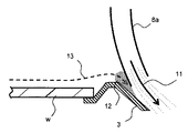
そこで、図4に示すように、リング状シャワーヘッド8により別途水素ガスを、例えば流量:15SLM、圧力:約0.2MPaで供給して、反応ガス流の外周側に外周ガス流11を形成する。このとき、外周ガス流11は、外向きに外周ガスを噴出するように設けられたノズル8aより、ホルダー3のテーパー部分にぶつかり、強い下向きの流れを形成する。そして、図5に図4の部分拡大図を示すように、ベンチュリ効果により、外周に負圧領域12が形成されるため、シャワーヘッド7からの反応ガスの流れでウェーハから外周への流れが引き込まれ(引き込まれる流れ13)、ウェーハ周辺に安定した流れが形成される。
Therefore, as shown in FIG. 4, hydrogen gas is separately supplied from the ring-
そして、ガス排出口6から排出されるガスの流量を所定の流量に制御することにより、反応室1内の圧力を、例えば1333Pa(10Torr)〜常圧となるように制御する。
Then, by controlling the flow rate of the gas discharged from the
そして、ウェーハwの温度が、面内で均一に、例えば1100℃となるように、ヒータ2を制御する。そして、回転機構4によりウェーハwを高速回転させて、ウェーハw上にSiエピタキシャル膜を形成する。
Then, the heater 2 is controlled so that the temperature of the wafer w is uniformly 1100 ° C. within the surface, for example. Then, the wafer w is rotated at a high speed by the
このようにして、シャワーヘッド7から供給される反応ガス流におけるH2のような軽いガスによる淀んだ流れを、その外周側に別途外周ガス流を形成し、ベンチュリ効果により整流することにより、一定の均一性を持つ反応ガス流を供給することができる。従って、例えばばらつきを従来の2%から1%に抑え、より均一に成膜することが可能となる。
In this way, the stagnant flow caused by a light gas such as H 2 in the reaction gas flow supplied from the
本実施形態において、リング状シャワーヘッド8より水素ガスを供給しているが、プロセス上問題が発生しないガスであれば用いることが可能である。プロセスコストの観点からは、水素ガス、ヘリウムガスなどが好適に用いられる。また、Arガスなどの比較的重い不活性ガスを用いることも効果的であり、減圧下であれば、適用も可能である。
In this embodiment, hydrogen gas is supplied from the ring-
また、反応ガス流と、外周ガス流の流量比は、流量バランスが取れ、良好な膜厚均一性を得る上で、
1/2≦(外周ガス流量/反応ガス流量)≦1
であることが好ましい。但し、外周ガスにキャリアガスと比較して重いArガスなどを用いる場合では、外周ガスの流量を抑えることが可能である。
In addition, the flow rate ratio between the reaction gas flow and the peripheral gas flow is balanced, and good film thickness uniformity is obtained.
1/2 ≦ (outer peripheral gas flow rate / reactive gas flow rate) ≦ 1
It is preferable that However, in the case where Ar gas, which is heavier than the carrier gas, is used as the peripheral gas, the flow rate of the peripheral gas can be suppressed.
また、リング状シャワーヘッド8の形状は外周に強い流れを作ることができれば、特に限定されるものではなく、例えば、図6に示すように、上方3箇所に外周ガス流用ガスを導入する外周ガス導入口18bが配置されたリング状のヘッド18cの下方に複数のノズル18aが配置された形状のリング状シャワーヘッド18を用いることができる。
The shape of the ring-
本実施形態によれば、ウェーハおよびウェーハより素子形成工程および素子分離工程を経て形成される半導体装置において、1ウェーハに形成されるチップ数を増大させ、歩留りを向上させるとともに、素子特性を安定させることが可能となる。特に、N型ベース領域、P型ベース領域や、絶縁分離領域などに数10μm〜100μm程度の厚膜が用いられるパワーMOSFETやIGBT(絶縁ゲート型バイポーラトランジスタ)などのパワー半導体装置の厚膜形成プロセスに適用することにより、プロセスコストの大幅な削減が可能となる。 According to this embodiment, in a semiconductor device formed from a wafer and a wafer through an element formation process and an element isolation process, the number of chips formed on one wafer is increased, yield is improved, and element characteristics are stabilized. It becomes possible. In particular, a thick film formation process of a power semiconductor device such as a power MOSFET or IGBT (insulated gate bipolar transistor) in which a thick film of about several tens to 100 μm is used for an N-type base region, a P-type base region, an insulating isolation region, and the like. By applying to the above, the process cost can be greatly reduced.
尚、本発明は、上述した実施形態に限定されるものではない。例えば、本実施形態においては、Si基板上にエピタキシャル膜形成の場合を説明したが、ポリSi層形成時にも適用でき、他の化合物半導体例えばGaAs層、GaAlAsやInGaAsなどにも適用可能である。また、SiO2膜やSi3N4膜形成の場合にも適用可能で、SiO2膜の場合、モノシラン(SiH4)の他、N2、O2、Arガスを、Si3N4膜の場合、モノシラン(SiH4)の他、NH3、N2、O2、Arガスなどを供給することになる。その他要旨を逸脱しない範囲で種々変形して実施することができる。 In addition, this invention is not limited to embodiment mentioned above. For example, although the case where an epitaxial film is formed on a Si substrate has been described in the present embodiment, the present invention can be applied to the formation of a poly-Si layer, and can be applied to other compound semiconductors such as a GaAs layer, GaAlAs, InGaAs, and the like. Further, the present invention can be applied to the case of forming a SiO 2 film or a Si 3 N 4 film. In the case of a SiO 2 film, in addition to monosilane (SiH 4 ), N 2 , O 2 , and Ar gas are used as the Si 3 N 4 film. In this case, NH 3 , N 2 , O 2 , Ar gas and the like are supplied in addition to monosilane (SiH 4 ). Various other modifications can be made without departing from the scope of the invention.
1…反応室、2…ヒータ、3…ホルダー、4…回転機構、5…反応ガス導入口、6…ガス排出口、7…シャワーヘッド、8、18…リング状シャワーヘッド、9…淀んだ流れ、10…流れが乱される領域、11…外周ガス流、12…負圧領域、13…引き込まれる流れ
DESCRIPTION OF SYMBOLS 1 ... Reaction chamber, 2 ... Heater, 3 ... Holder, 4 ... Rotation mechanism, 5 ... Reaction gas introduction port, 6 ... Gas discharge port, 7 ... Shower head, 8, 18 ... Ring-shaped shower head, 9 ... Stagnant flow DESCRIPTION OF
Claims (5)
前記ウェーハを回転させながら裏面より加熱し、
前記ウェーハを保持する保持機構の上面の外周部に対してノズルの先端部が離間して近傍に配置されたシャワーヘッドの内側において、前記ウェーハの上方より、前記ウェーハの全面に前記反応ガスを供給するための第1のガス流を形成するとともに、前記ノズルと前記保持機構との隙間から流出する前記第1のガス流の外周に、前記ノズルからのガス供給によって外周下方向の第2のガス流を形成して、前記ウェーハ上に成膜を行うことを特徴とする気相成長方法。 Introduce reaction gas into the reaction chamber for film formation on the wafer,
Heat from the back while rotating the wafer,
Provided at the inner side of the shower head tip of the nozzle with respect to the outer peripheral portion of the upper surface of the holding mechanism is disposed near and spaced apart for holding the wafer, from above the wafer, the reaction gas to the entire surface of the wafer A second gas in the downward direction of the outer periphery by supplying gas from the nozzle to the outer periphery of the first gas flow that flows out from the gap between the nozzle and the holding mechanism. A vapor phase growth method characterized in that a flow is formed to form a film on the wafer.
1/2≦(第2のガス流量/第1のガス流量)≦1
であることを特徴とする請求項1または請求項2に記載の気相成長装置。 The flow rate ratio between the first gas flow and the second gas flow is:
1/2 ≦ (second gas flow rate / first gas flow rate) ≦ 1
The vapor phase growth apparatus according to claim 1 or 2, wherein
前記反応室下部に設けられ、前記ウェーハを加熱するヒータと、
前記ウェーハを保持する保持機構と、
前記保持機構と接続され、前記ウェーハを回転させる回転機構と、
前記反応室の上部に設けられ、上方より前記ウェーハ全面に供給される反応ガスによる第1のガス流を形成する第1のガス供給機構と、
前記保持機構の上面の外周部に対してノズルの先端部が離間して近傍に配置され、前記ノズルと前記保持機構との隙間から流出する前記反応ガスのガス流の外周に、前記ノズルからのガス供給によって外周下方向の第2のガス流を形成する第2のガス供給機構と、
を備えることを特徴とする気相成長装置。 And line cormorant anti応室the deposition on the wafer,
Provided in the lower part the reaction chamber, and Ruhi over data to heat said wafer,
A hold mechanism that holds the wafer,
Is connected to the holding mechanism, a rotating mechanism you want to rotate. The wafer,
Provided in an upper portion of said reaction chamber, a first gas supply mechanism that form a first gas stream by the reaction gas supplied to the entire wafer surface from above,
The tip of the nozzle is disposed in the vicinity of the outer peripheral portion of the upper surface of the holding mechanism, and is disposed in the vicinity of the gas flow of the reaction gas flowing out from the gap between the nozzle and the holding mechanism . a second gas supply mechanism that form a second gas flow in the lower peripheral direction by the gas supply,
A vapor phase growth apparatus comprising:
Priority Applications (1)
| Application Number | Priority Date | Filing Date | Title |
|---|---|---|---|
| JP2007054424A JP4981485B2 (en) | 2007-03-05 | 2007-03-05 | Vapor phase growth method and vapor phase growth apparatus |
Applications Claiming Priority (1)
| Application Number | Priority Date | Filing Date | Title |
|---|---|---|---|
| JP2007054424A JP4981485B2 (en) | 2007-03-05 | 2007-03-05 | Vapor phase growth method and vapor phase growth apparatus |
Publications (2)
| Publication Number | Publication Date |
|---|---|
| JP2008218734A JP2008218734A (en) | 2008-09-18 |
| JP4981485B2 true JP4981485B2 (en) | 2012-07-18 |
Family
ID=39838415
Family Applications (1)
| Application Number | Title | Priority Date | Filing Date |
|---|---|---|---|
| JP2007054424A Expired - Fee Related JP4981485B2 (en) | 2007-03-05 | 2007-03-05 | Vapor phase growth method and vapor phase growth apparatus |
Country Status (1)
| Country | Link |
|---|---|
| JP (1) | JP4981485B2 (en) |
Families Citing this family (10)
| Publication number | Priority date | Publication date | Assignee | Title |
|---|---|---|---|---|
| JP2010186949A (en) * | 2009-02-13 | 2010-08-26 | Nuflare Technology Inc | Semiconductor manufacturing apparatus and semiconductor manufacturing method |
| JP5410348B2 (en) | 2010-03-26 | 2014-02-05 | 株式会社豊田中央研究所 | Surface treatment equipment |
| JP6134522B2 (en) * | 2013-01-30 | 2017-05-24 | 株式会社ニューフレアテクノロジー | Vapor growth apparatus and vapor growth method |
| JP6199619B2 (en) * | 2013-06-13 | 2017-09-20 | 株式会社ニューフレアテクノロジー | Vapor growth equipment |
| JP6226677B2 (en) * | 2013-10-02 | 2017-11-08 | 株式会社ニューフレアテクノロジー | Semiconductor manufacturing apparatus and semiconductor manufacturing method |
| JP5837962B1 (en) | 2014-07-08 | 2015-12-24 | 株式会社日立国際電気 | Substrate processing apparatus, semiconductor device manufacturing method, and gas rectifier |
| JP6881283B2 (en) * | 2017-12-27 | 2021-06-02 | 株式会社Sumco | Manufacturing method of epitaxial silicon wafer and epitaxial silicon wafer |
| CN112813414B (en) * | 2020-12-30 | 2022-12-09 | 上海埃延半导体有限公司 | Chemical vapor deposition system |
| CN118835312B (en) * | 2024-09-23 | 2025-10-17 | 瑶光半导体(浙江)有限公司 | Reaction chamber of epitaxial process and multi-piece planetary epitaxial equipment |
| CN118835313B (en) * | 2024-09-24 | 2025-10-17 | 瑶光半导体(浙江)有限公司 | Epitaxial device, air inlet method thereof, readable storage medium and computer device |
Family Cites Families (6)
| Publication number | Priority date | Publication date | Assignee | Title |
|---|---|---|---|---|
| JPH04348031A (en) * | 1990-12-28 | 1992-12-03 | Mitsubishi Electric Corp | Chemical vapor growth equipment |
| JPH08255792A (en) * | 1995-03-16 | 1996-10-01 | Toshiba Corp | Method for manufacturing semiconductor device |
| KR100331544B1 (en) * | 1999-01-18 | 2002-04-06 | 윤종용 | Method for introducing gases into a reactor chamber and a shower head used therein |
| JP2001267248A (en) * | 2000-03-15 | 2001-09-28 | Shibaura Mechatronics Corp | Semiconductor processing equipment |
| JP2002110567A (en) * | 2000-10-03 | 2002-04-12 | Mitsubishi Electric Corp | Chemical vapor deposition apparatus and method for forming semiconductor wafer by using the apparatus |
| JP2004035971A (en) * | 2002-07-05 | 2004-02-05 | Ulvac Japan Ltd | Thin film manufacturing apparatus |
-
2007
- 2007-03-05 JP JP2007054424A patent/JP4981485B2/en not_active Expired - Fee Related
Also Published As
| Publication number | Publication date |
|---|---|
| JP2008218734A (en) | 2008-09-18 |
Similar Documents
| Publication | Publication Date | Title |
|---|---|---|
| JP4981485B2 (en) | Vapor phase growth method and vapor phase growth apparatus | |
| KR101154639B1 (en) | Semiconductor manufacturing apparatus and semiconductor manufacturing method | |
| KR100907148B1 (en) | Film forming apparatus and film forming method | |
| JP5413305B2 (en) | Epitaxial growth equipment | |
| JP6153401B2 (en) | Vapor growth apparatus and vapor growth method | |
| JP4956470B2 (en) | Semiconductor manufacturing apparatus and semiconductor manufacturing method | |
| JP7365761B2 (en) | Vapor phase growth equipment | |
| US11692266B2 (en) | SiC chemical vapor deposition apparatus | |
| US7923355B2 (en) | Manufacturing method for semiconductor device and manufacturing apparatus for semiconductor device | |
| JP5443096B2 (en) | Semiconductor manufacturing apparatus and semiconductor manufacturing method | |
| TWI548772B (en) | Semiconductor manufacturing device and semiconductor manufacturing method | |
| JP2008198752A (en) | Vapor growth apparatus and vapor growth method | |
| CN107546101A (en) | A kind of epitaxial growth method | |
| JP5443223B2 (en) | Vapor growth apparatus and method for manufacturing nitride semiconductor light emitting device | |
| JP2011151118A (en) | Apparatus and method for manufacturing semiconductor | |
| CN100459033C (en) | Film forming method and film forming apparatus | |
| JP2010186949A (en) | Semiconductor manufacturing apparatus and semiconductor manufacturing method | |
| WO2018008334A1 (en) | Gas piping system, chemical vapor deposition device, film deposition method, and method for producing sic epitaxial wafer | |
| JP5134311B2 (en) | Semiconductor manufacturing apparatus and semiconductor manufacturing method | |
| JP2008243938A (en) | Thermal CVD method and thermal CVD apparatus | |
| JP2009010279A (en) | Thin film manufacturing device | |
| JP2004014535A (en) | Vapor phase growth apparatus, vapor phase growth method, and susceptor for holding substrate | |
| JP2007180528A (en) | Film forming method and film forming apparatus | |
| JP2008205018A (en) | Vapor phase growth method and vapor phase growth apparatus | |
| JPH05121337A (en) | Method for gas reaction on solid surface |
Legal Events
| Date | Code | Title | Description |
|---|---|---|---|
| A621 | Written request for application examination |
Free format text: JAPANESE INTERMEDIATE CODE: A621 Effective date: 20090820 |
|
| A977 | Report on retrieval |
Free format text: JAPANESE INTERMEDIATE CODE: A971007 Effective date: 20091110 |
|
| A131 | Notification of reasons for refusal |
Free format text: JAPANESE INTERMEDIATE CODE: A131 Effective date: 20120124 |
|
| A521 | Written amendment |
Free format text: JAPANESE INTERMEDIATE CODE: A523 Effective date: 20120323 |
|
| TRDD | Decision of grant or rejection written | ||
| A01 | Written decision to grant a patent or to grant a registration (utility model) |
Free format text: JAPANESE INTERMEDIATE CODE: A01 Effective date: 20120410 |
|
| A01 | Written decision to grant a patent or to grant a registration (utility model) |
Free format text: JAPANESE INTERMEDIATE CODE: A01 |
|
| A61 | First payment of annual fees (during grant procedure) |
Free format text: JAPANESE INTERMEDIATE CODE: A61 Effective date: 20120420 |
|
| FPAY | Renewal fee payment (event date is renewal date of database) |
Free format text: PAYMENT UNTIL: 20150427 Year of fee payment: 3 |
|
| R150 | Certificate of patent or registration of utility model |
Free format text: JAPANESE INTERMEDIATE CODE: R150 Ref document number: 4981485 Country of ref document: JP Free format text: JAPANESE INTERMEDIATE CODE: R150 |
|
| S531 | Written request for registration of change of domicile |
Free format text: JAPANESE INTERMEDIATE CODE: R313531 |
|
| R350 | Written notification of registration of transfer |
Free format text: JAPANESE INTERMEDIATE CODE: R350 |
|
| R250 | Receipt of annual fees |
Free format text: JAPANESE INTERMEDIATE CODE: R250 |
|
| R250 | Receipt of annual fees |
Free format text: JAPANESE INTERMEDIATE CODE: R250 |
|
| R250 | Receipt of annual fees |
Free format text: JAPANESE INTERMEDIATE CODE: R250 |
|
| R250 | Receipt of annual fees |
Free format text: JAPANESE INTERMEDIATE CODE: R250 |
|
| R250 | Receipt of annual fees |
Free format text: JAPANESE INTERMEDIATE CODE: R250 |
|
| R250 | Receipt of annual fees |
Free format text: JAPANESE INTERMEDIATE CODE: R250 |
|
| LAPS | Cancellation because of no payment of annual fees |