JP4982237B2 - 高周波回路 - Google Patents
高周波回路 Download PDFInfo
- Publication number
- JP4982237B2 JP4982237B2 JP2007110594A JP2007110594A JP4982237B2 JP 4982237 B2 JP4982237 B2 JP 4982237B2 JP 2007110594 A JP2007110594 A JP 2007110594A JP 2007110594 A JP2007110594 A JP 2007110594A JP 4982237 B2 JP4982237 B2 JP 4982237B2
- Authority
- JP
- Japan
- Prior art keywords
- case
- multilayer substrate
- ground conductor
- frequency circuit
- conductor layer
- Prior art date
- Legal status (The legal status is an assumption and is not a legal conclusion. Google has not performed a legal analysis and makes no representation as to the accuracy of the status listed.)
- Active
Links
Images



Landscapes
- Microwave Amplifiers (AREA)
Description
したがって、筐体と多層基板の間を高周波的に同電位に保つことができ、高周波特性を安定させることができる。このため、高周波回路を所定の入力回路や所定の出力回路に接続した場合に入力回路から高周波回路に信号が入力したときに、高周波回路から出力回路に送信される信号のばらつき等が発生するのを防止することができる。
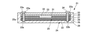
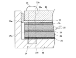
図1〜図4は本発明に係る高周波回路の一実施の形態を示す図である。
まず、構成を説明する。
このため、固体電力増幅器21にODUに設けられる周波数変換回路等から信号が入力した場合に、この信号のばらつきが発生するのを防止して、所定の出力回路に送信することができる。
22 ケース(筐体)
22a 開口部
23 蓋(閉塞部材、筐体)
24 筐体
25 多層基板
26、27 絶縁層
28 高周波信号線路
29、30 接地導体層(誘電体)
31 凹部
32 増幅素子(半導体素子)
33 バネシート(弾性シート)
33a 曲げ部
33c、33d 舌部(接触部)
34 ネジ(固定手段)
Claims (2)
- 一端が開口する有底状のケースおよび前記開口を閉塞するように前記ケースに取付けられた閉塞部材を有する筐体と、上下の接地導体層に挟まれた誘電体中にストリップ線路による高周波信号線路を有し、一方の接地導体層が前記ケースに接触するようにして前記ケースに収納される多層基板と、前記閉塞部材を前記ケースに固定する固定手段とを備えた高周波回路において、
他方の接地導体層と接触するように前記多層基板と前記閉塞部材の間に金属製の弾性シートを介装し、前記閉塞部材が前記弾性シートを介して前記多層基板を前記ケースの底面に向かって押圧し、
前記多層基板は、他方の接地導体層および誘電体の一部を貫通する凹部を有し、前記凹部の底面に前記高周波信号線路を露出させるとともに、前記高周波信号線路に接続されるように前記凹部に半導体素子が収容され、
前記弾性シートは、前記半導体素子の上面に接触する接触部を有することを特徴とする高周波回路。 - 前記弾性シートの面積は、前記ケースの開口面積よりも大きく形成されるとともに、前記弾性シートの外周部に折り曲げ部が設けられ、前記折り曲げ部は、前記ケースの内周部に接触することを特徴とする請求項1に記載の高周波回路。
Priority Applications (1)
| Application Number | Priority Date | Filing Date | Title |
|---|---|---|---|
| JP2007110594A JP4982237B2 (ja) | 2007-04-19 | 2007-04-19 | 高周波回路 |
Applications Claiming Priority (1)
| Application Number | Priority Date | Filing Date | Title |
|---|---|---|---|
| JP2007110594A JP4982237B2 (ja) | 2007-04-19 | 2007-04-19 | 高周波回路 |
Publications (2)
| Publication Number | Publication Date |
|---|---|
| JP2008270481A JP2008270481A (ja) | 2008-11-06 |
| JP4982237B2 true JP4982237B2 (ja) | 2012-07-25 |
Family
ID=40049604
Family Applications (1)
| Application Number | Title | Priority Date | Filing Date |
|---|---|---|---|
| JP2007110594A Active JP4982237B2 (ja) | 2007-04-19 | 2007-04-19 | 高周波回路 |
Country Status (1)
| Country | Link |
|---|---|
| JP (1) | JP4982237B2 (ja) |
Families Citing this family (1)
| Publication number | Priority date | Publication date | Assignee | Title |
|---|---|---|---|---|
| JP5093138B2 (ja) * | 2009-02-02 | 2012-12-05 | 三菱電機株式会社 | マイクロ波送受信モジュール |
Family Cites Families (9)
| Publication number | Priority date | Publication date | Assignee | Title |
|---|---|---|---|---|
| JPS6144901U (ja) * | 1984-08-27 | 1986-03-25 | 日本電気株式会社 | マイクロ波回路構造 |
| JPH04563Y2 (ja) * | 1985-09-02 | 1992-01-09 | ||
| JPS62219697A (ja) * | 1986-03-20 | 1987-09-26 | 松下電器産業株式会社 | マイクロ波装置 |
| JPS62237802A (ja) * | 1986-04-09 | 1987-10-17 | Matsushita Electric Ind Co Ltd | ストリツプラインフイルタ |
| JPS6361180U (ja) * | 1986-10-08 | 1988-04-22 | ||
| JPH07283573A (ja) * | 1994-04-12 | 1995-10-27 | Nec Corp | シールド装置 |
| JPH09321501A (ja) * | 1996-05-30 | 1997-12-12 | Mitsubishi Electric Corp | 多層高周波回路基板 |
| JP2000106493A (ja) * | 1998-09-28 | 2000-04-11 | Matsushita Electric Ind Co Ltd | 電子機器 |
| JP3410673B2 (ja) * | 1999-03-15 | 2003-05-26 | 日本無線株式会社 | 半導体装置及び半導体チップの実装方法 |
-
2007
- 2007-04-19 JP JP2007110594A patent/JP4982237B2/ja active Active
Also Published As
| Publication number | Publication date |
|---|---|
| JP2008270481A (ja) | 2008-11-06 |
Similar Documents
| Publication | Publication Date | Title |
|---|---|---|
| JP4684730B2 (ja) | 高周波半導体装置、送信装置および受信装置 | |
| JP5426072B2 (ja) | 自動車レーダセンサアセンブリ | |
| US9117835B2 (en) | Highly integrated miniature radio frequency module | |
| US9515385B2 (en) | Coplanar waveguide implementing launcher and waveguide channel section in IC package substrate | |
| EP3361570B1 (en) | Split ring resonator antenna | |
| JP4645664B2 (ja) | 高周波装置 | |
| EP2330683A1 (en) | In-millimeter-wave dielectric transmission device and method for manufacturing same, and wireless transmission device and wireless transmission method | |
| US7019600B2 (en) | Waveguide/planar line converter and high frequency circuit arrangement | |
| US20150270616A1 (en) | Rf system-in-package with quasi-coaxial coplanar waveguide transition | |
| EP2889952B1 (en) | Semiconductor package and semiconductor module | |
| KR20220032895A (ko) | 안테나 장치 | |
| US8035994B2 (en) | High frequency storing case and high frequency module | |
| JP5342995B2 (ja) | 高周波モジュール | |
| US8040684B2 (en) | Package for electronic component and method for manufacturing the same | |
| JP2010272959A (ja) | 高周波回路、低雑音ダウンコンバータおよびアンテナ装置 | |
| JP2008270481A (ja) | 高周波回路 | |
| JP2005183410A (ja) | 無線回路モジュールおよび無線回路基板 | |
| JP2009302603A (ja) | 高周波装置 | |
| US12003045B2 (en) | Wireless interconnect for high rate data transfer | |
| JP2009159203A (ja) | 誘電体レンズ付きアンテナ | |
| JP2001177312A (ja) | 高周波接続モジュール | |
| US10483632B2 (en) | Device for transmitting and/or receiving radiofrequency signals | |
| KR20220069850A (ko) | 안테나 디바이스 | |
| JP2006067375A (ja) | アンテナモジュール | |
| JP3344388B2 (ja) | マイクロ波導波管装置 |
Legal Events
| Date | Code | Title | Description |
|---|---|---|---|
| A621 | Written request for application examination |
Free format text: JAPANESE INTERMEDIATE CODE: A621 Effective date: 20100419 |
|
| A977 | Report on retrieval |
Free format text: JAPANESE INTERMEDIATE CODE: A971007 Effective date: 20110621 |
|
| A131 | Notification of reasons for refusal |
Free format text: JAPANESE INTERMEDIATE CODE: A131 Effective date: 20110628 |
|
| A521 | Request for written amendment filed |
Free format text: JAPANESE INTERMEDIATE CODE: A523 Effective date: 20110729 |
|
| TRDD | Decision of grant or rejection written | ||
| A01 | Written decision to grant a patent or to grant a registration (utility model) |
Free format text: JAPANESE INTERMEDIATE CODE: A01 Effective date: 20120403 |
|
| A01 | Written decision to grant a patent or to grant a registration (utility model) |
Free format text: JAPANESE INTERMEDIATE CODE: A01 |
|
| A61 | First payment of annual fees (during grant procedure) |
Free format text: JAPANESE INTERMEDIATE CODE: A61 Effective date: 20120423 |
|
| FPAY | Renewal fee payment (event date is renewal date of database) |
Free format text: PAYMENT UNTIL: 20150427 Year of fee payment: 3 |
|
| R150 | Certificate of patent or registration of utility model |
Ref document number: 4982237 Country of ref document: JP Free format text: JAPANESE INTERMEDIATE CODE: R150 Free format text: JAPANESE INTERMEDIATE CODE: R150 |