JP4982446B2 - 液晶表示装置 - Google Patents
液晶表示装置 Download PDFInfo
- Publication number
- JP4982446B2 JP4982446B2 JP2008186683A JP2008186683A JP4982446B2 JP 4982446 B2 JP4982446 B2 JP 4982446B2 JP 2008186683 A JP2008186683 A JP 2008186683A JP 2008186683 A JP2008186683 A JP 2008186683A JP 4982446 B2 JP4982446 B2 JP 4982446B2
- Authority
- JP
- Japan
- Prior art keywords
- fluorescent tube
- tube support
- liquid crystal
- crystal display
- lss
- Prior art date
- Legal status (The legal status is an assumption and is not a legal conclusion. Google has not performed a legal analysis and makes no representation as to the accuracy of the status listed.)
- Expired - Fee Related
Links
Images


Classifications
-
- G—PHYSICS
- G02—OPTICS
- G02F—OPTICAL DEVICES OR ARRANGEMENTS FOR THE CONTROL OF LIGHT BY MODIFICATION OF THE OPTICAL PROPERTIES OF THE MEDIA OF THE ELEMENTS INVOLVED THEREIN; NON-LINEAR OPTICS; FREQUENCY-CHANGING OF LIGHT; OPTICAL LOGIC ELEMENTS; OPTICAL ANALOGUE/DIGITAL CONVERTERS
- G02F1/00—Devices or arrangements for the control of the intensity, colour, phase, polarisation or direction of light arriving from an independent light source, e.g. switching, gating or modulating; Non-linear optics
- G02F1/01—Devices or arrangements for the control of the intensity, colour, phase, polarisation or direction of light arriving from an independent light source, e.g. switching, gating or modulating; Non-linear optics for the control of the intensity, phase, polarisation or colour
- G02F1/13—Devices or arrangements for the control of the intensity, colour, phase, polarisation or direction of light arriving from an independent light source, e.g. switching, gating or modulating; Non-linear optics for the control of the intensity, phase, polarisation or colour based on liquid crystals, e.g. single liquid crystal display cells
- G02F1/133—Constructional arrangements; Operation of liquid crystal cells; Circuit arrangements
- G02F1/1333—Constructional arrangements; Manufacturing methods
- G02F1/1335—Structural association of cells with optical devices, e.g. polarisers or reflectors
- G02F1/1336—Illuminating devices
- G02F1/133602—Direct backlight
- G02F1/133608—Direct backlight including particular frames or supporting means
-
- G—PHYSICS
- G02—OPTICS
- G02F—OPTICAL DEVICES OR ARRANGEMENTS FOR THE CONTROL OF LIGHT BY MODIFICATION OF THE OPTICAL PROPERTIES OF THE MEDIA OF THE ELEMENTS INVOLVED THEREIN; NON-LINEAR OPTICS; FREQUENCY-CHANGING OF LIGHT; OPTICAL LOGIC ELEMENTS; OPTICAL ANALOGUE/DIGITAL CONVERTERS
- G02F1/00—Devices or arrangements for the control of the intensity, colour, phase, polarisation or direction of light arriving from an independent light source, e.g. switching, gating or modulating; Non-linear optics
- G02F1/01—Devices or arrangements for the control of the intensity, colour, phase, polarisation or direction of light arriving from an independent light source, e.g. switching, gating or modulating; Non-linear optics for the control of the intensity, phase, polarisation or colour
- G02F1/13—Devices or arrangements for the control of the intensity, colour, phase, polarisation or direction of light arriving from an independent light source, e.g. switching, gating or modulating; Non-linear optics for the control of the intensity, phase, polarisation or colour based on liquid crystals, e.g. single liquid crystal display cells
- G02F1/133—Constructional arrangements; Operation of liquid crystal cells; Circuit arrangements
- G02F1/1333—Constructional arrangements; Manufacturing methods
- G02F1/1335—Structural association of cells with optical devices, e.g. polarisers or reflectors
- G02F1/1336—Illuminating devices
- G02F1/133602—Direct backlight
- G02F1/133604—Direct backlight with lamps
Landscapes
- Physics & Mathematics (AREA)
- Nonlinear Science (AREA)
- Mathematical Physics (AREA)
- Chemical & Material Sciences (AREA)
- Crystallography & Structural Chemistry (AREA)
- General Physics & Mathematics (AREA)
- Optics & Photonics (AREA)
- Liquid Crystal (AREA)
- Planar Illumination Modules (AREA)
- Fastening Of Light Sources Or Lamp Holders (AREA)
- Arrangement Of Elements, Cooling, Sealing, Or The Like Of Lighting Devices (AREA)
Description
前記バックライトは、少なくとも、前記液晶表示パネルと対向する面内に並設された複数の線状蛍光管と、前記線状蛍光管を支持する蛍光管支持台と、前記蛍光管支持台が固定されるフレームを備え、
前記蛍光管支持台は、平板状の基板を備え、該基板の中央に円錐状の柱状体の光学シート支持柱が形成され、該光学シート支持柱の両脇に前記基板の表面から所定の高さで形成された台座の上面に形成され、前記線状蛍光管の管側面を押圧する管挟持部と前記線状蛍光管の挿入を容易にする管挿入口部を有する前記線状蛍光管を保持する蛍光管支持材と、前記フレームに前記蛍光管支持台を固定するための係止部を備え、
前記係止部は前記蛍光管支持材に重畳しない位置であり、前記蛍光管支持材よりも前記基板の端部側に形成され、
前記フレームは、前記蛍光管支持材と重畳し、前記係止部と重畳しない位置に凹陥部が形成されることを特徴とする。
〈全体構成〉
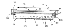
図2は、本発明による液晶表示装置の一実施例を示す概略構成図である。
液晶表示装置は、図3に示すように、バックライトBLの下フレームDFRに対して積層して配置される上フレームUFRおよび中間フレームMFRを有し、上フレームUFRと中間フレームMFR間に液晶表示パネルPNL、光学シートOSを配置してモジュール化されている。なお、図3は図2のIII−III線に相当する個所の断面を示している。上フレームUFRは、観察者側において、少なくとも液晶表示パネルPNLの液晶表示領域ARを露出させる開口OPが形成されている。また、液晶表示パネルPNLの基板SUB1に接続された半導体装置SCDは、そのフレキシブル基板FBの個所で直交するように折り曲げられ、下フレームDFRの側面に配置させる。いわゆる狭額縁化を図るためである。
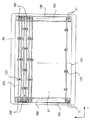
図4は、図2に示した前記バックライトBLのみを抜き出して示した拡大図である。図4では、図2に示されていなかった蛍光管支持台LSSが描かれている。該蛍光管支持台LSSは、下フレームDFRに固定され、外部電極蛍光管EFLの管部を支持するように設けられている。外部電極蛍光管EFLは、その両端の電極の部分においても、電極金具TMF(図6参照)を介して下フレームDFRに支持されている。しかし、液晶表示装置の大型化に伴い、長い外部電極蛍光管EFLが用いられると、電極の部分のみでは充分な支持ができなくなるため、蛍光管の中間部分である管部をも支持するために、前記蛍光管支持台LSSが配置されるようになっている。図4に示す実施例では、1個の蛍光管支持台LSSにおいて、たとえば、隣接して並設される2本の外部電極蛍光管EFLを支持できるように構成され、当該外部電極蛍光管EFLの長手方向に沿ってたとえば等間隔に複数の蛍光管支持台LSSを配置させている。また、上述した2本の外部電極蛍光管EFLに隣接して配置される他の2本の外部電極蛍光管EFLにおいても、その長手方向に沿って複数の蛍光管支持台LSSによって支持されているが、これらの蛍光管支持台LSSは、上述した2本の外部電極蛍光管EFLを支持する蛍光管支持台LSSに対して、ずらした位置に配置させた構成となっている。蛍光管支持台LSSが一列に並んでしまうと、その部分の輝度が低下するため、それを回避するためである。
図6(a)は、前記電極支持材TMSの一実施例を示した平面図で、図5の点線枠Qの部分を拡大して示した図である。図6(a)において、電極支持材TMSは、並設される3個の電極金具TMFを共通に固定する基部BPと、この基部BPの各端側に接続する左側接続部JC(L)と右側接続部JC(R)とを有し、これら基部BPと各接続部JC(L)、JC(R)は、平面的に観た場合、梯子状のパターンをなして形成されている。
図7は、前記蛍光管支持台LSSを示す構成図で、図4にて点線丸枠S枠内に示した蛍光管支持台LSSを示している。図7に示す該蛍光管支持台LSSは、下フレームDFRに取り付けられていない状態である。
ここで、外部電極蛍光管EFLに蛍光管支持台LSSが密着していない場合と等価の熱抵抗に近づけるための、図1に示した下フレームDFRの凹陥部DNTの深さ、すなわち空気層の層厚について考察する。
ここで、Lは熱の伝導方向における熱源に接触する材料の長さ、λは熱源に接触する材料の熱伝導率、Aは熱源とそれに接触する材料との接触面積である。
Rx = Ra − Rp …… (2)
蛍光管支持台LSSの熱伝導率をλp、空気層の熱伝導率をλaとし、式(2)に式(1)を代入すると、次式(3)を得る。
ここで、本実施例においては、蛍光管支持台LSSに用いる樹脂の熱伝導率λpを0.23、空気層の熱伝導率λaを0.02614とする。これらの熱伝導率の数値を式(3)に代入することによって、次式(4)を得る。
すなわち、式(4)によれば、凹陥部DNTの深さLxは、蛍光管支持台LSSの高さの約9割以上であればよいことが分かる。このため、現実的には、下フレームDFRの凹陥部DNTの深さ(空気層厚)を、蛍光管支持台LSSの高さとほぼ等しくする(Lx≒L1)すれば、該蛍光管支持台LSSを取り付けない場合と熱的状態が十分に同等にできる。
図8は、本発明の実施例2を示す図で、蛍光管支持台LSSの他の実施例を図1と対応させて示している。
図9は、本発明の実施例3を示す図で、蛍光管支持台LSSの他の実施例を示している。
図10は、本発明の実施例4を示す図で、蛍光管支持台LSSの他の実施例を示している。図8(a)の場合と比較して異なる構成は、蛍光管支持材LSMおよび台座SSにある。
図11は、本発明の実施例5を示す図で、蛍光管支持台LSSの他の実施例を示している。図11(a)は蛍光管支持台LSSの長辺方向の側面側から観た図、図11(b)は蛍光管支持台LSSの短辺方向の側面側から観た図、図11(c)は蛍光管支持台LSSを上から見た平面図である。
Claims (2)
- 液晶表示パネルと、前記液晶表示パネルを照射するための光源を備えたバックライトを備え、
前記バックライトは、少なくとも、前記液晶表示パネルと対向する面内に並設された複数の線状蛍光管と、前記線状蛍光管を支持する蛍光管支持台と、前記蛍光管支持台が固定されるフレームを備え、
前記蛍光管支持台は、平板状の基板を備え、該基板の中央に円錐状の柱状体の光学シート支持柱が形成され、該光学シート支持柱の両脇に前記基板の表面から所定の高さで形成された台座の上面に形成され、前記線状蛍光管の管側面を押圧する管挟持部と前記線状蛍光管の挿入を容易にする管挿入口部を有する前記線状蛍光管を保持する蛍光管支持材と、前記フレームに前記蛍光管支持台を固定するための係止部を備え、
前記係止部は前記蛍光管支持材に重畳しない位置であり、前記蛍光管支持材よりも前記基板の端部側に形成され、
前記フレームは、前記蛍光管支持材と重畳し、前記係止部と重畳しない位置に凹陥部が形成されることを特徴とする液晶表示装置。 - 前記凹陥部の深さは、前記フレームと前記線状蛍光管の間隔以上であることを特徴とする請求項1に記載の液晶表示装置。
Priority Applications (2)
| Application Number | Priority Date | Filing Date | Title |
|---|---|---|---|
| JP2008186683A JP4982446B2 (ja) | 2008-07-18 | 2008-07-18 | 液晶表示装置 |
| US12/505,039 US8228457B2 (en) | 2008-07-18 | 2009-07-17 | Liquid crystal display device |
Applications Claiming Priority (1)
| Application Number | Priority Date | Filing Date | Title |
|---|---|---|---|
| JP2008186683A JP4982446B2 (ja) | 2008-07-18 | 2008-07-18 | 液晶表示装置 |
Related Child Applications (1)
| Application Number | Title | Priority Date | Filing Date |
|---|---|---|---|
| JP2011044721A Division JP5242723B2 (ja) | 2011-03-02 | 2011-03-02 | 液晶表示装置 |
Publications (3)
| Publication Number | Publication Date |
|---|---|
| JP2010026186A JP2010026186A (ja) | 2010-02-04 |
| JP2010026186A5 JP2010026186A5 (ja) | 2010-08-12 |
| JP4982446B2 true JP4982446B2 (ja) | 2012-07-25 |
Family
ID=41530033
Family Applications (1)
| Application Number | Title | Priority Date | Filing Date |
|---|---|---|---|
| JP2008186683A Expired - Fee Related JP4982446B2 (ja) | 2008-07-18 | 2008-07-18 | 液晶表示装置 |
Country Status (2)
| Country | Link |
|---|---|
| US (1) | US8228457B2 (ja) |
| JP (1) | JP4982446B2 (ja) |
Families Citing this family (4)
| Publication number | Priority date | Publication date | Assignee | Title |
|---|---|---|---|---|
| JP5254591B2 (ja) * | 2007-10-25 | 2013-08-07 | 株式会社ジャパンディスプレイイースト | 液晶表示装置 |
| CN102159883A (zh) * | 2008-11-05 | 2011-08-17 | 夏普株式会社 | 支承单元、照明装置和显示装置 |
| KR101329077B1 (ko) * | 2008-12-09 | 2013-11-20 | 엘지디스플레이 주식회사 | 액정표시장치의 백라이트 유닛 및 그 조립방법 |
| JP6205647B2 (ja) * | 2014-05-23 | 2017-10-04 | コニカミノルタ株式会社 | 導光体、照明装置及び画像読み取り装置 |
Family Cites Families (8)
| Publication number | Priority date | Publication date | Assignee | Title |
|---|---|---|---|---|
| JP2001210126A (ja) | 2000-01-31 | 2001-08-03 | Sharp Corp | ランプホルダ及びバックライト装置 |
| JP4091519B2 (ja) * | 2003-04-25 | 2008-05-28 | ハリソン東芝ライティング株式会社 | バックライト装置 |
| JP2006039487A (ja) * | 2004-07-30 | 2006-02-09 | Hitachi Displays Ltd | 液晶表示装置 |
| JP4420848B2 (ja) | 2005-03-31 | 2010-02-24 | シャープ株式会社 | 蛍光管支持体、これを用いた直下式バックライト装置および直下式バックライト装置を用いた液晶表示装置 |
| TW200720762A (en) * | 2005-10-20 | 2007-06-01 | Samsung Electronics Co Ltd | Backlight assembly and display device having the same |
| CN100437282C (zh) * | 2005-10-21 | 2008-11-26 | 鸿富锦精密工业(深圳)有限公司 | 背光模组和其灯管夹持装置 |
| JP3992726B1 (ja) * | 2006-06-26 | 2007-10-17 | シャープ株式会社 | クリップ及び光源装置 |
| JP2008153161A (ja) * | 2006-12-20 | 2008-07-03 | Sharp Corp | 表示装置用照明装置、表示装置 |
-
2008
- 2008-07-18 JP JP2008186683A patent/JP4982446B2/ja not_active Expired - Fee Related
-
2009
- 2009-07-17 US US12/505,039 patent/US8228457B2/en not_active Expired - Fee Related
Also Published As
| Publication number | Publication date |
|---|---|
| US20100014017A1 (en) | 2010-01-21 |
| US8228457B2 (en) | 2012-07-24 |
| JP2010026186A (ja) | 2010-02-04 |
Similar Documents
| Publication | Publication Date | Title |
|---|---|---|
| JP4822953B2 (ja) | ボトムフレームと、これを利用したバックライトアセンブリ及び液晶表示装置 | |
| JP5079889B2 (ja) | 照明装置、表示装置及びテレビ受信装置 | |
| CN1591132B (zh) | 显示装置的背光组件 | |
| US9019443B2 (en) | Backlight unit comprising a plurality of slits formed on a bottom surface of at least one edge of a bottom cover and liquid crystal display device having the same | |
| JP5254591B2 (ja) | 液晶表示装置 | |
| US8218107B2 (en) | Backlight unit and liquid crystal display device including the same | |
| CN101929639A (zh) | 背光单元和具有该背光单元的液晶显示设备 | |
| JP4982446B2 (ja) | 液晶表示装置 | |
| JP2013088588A (ja) | 液晶表示装置 | |
| US7746419B2 (en) | Liquid crystal display device | |
| KR100923614B1 (ko) | 액정 표시 장치 | |
| JP2010122330A (ja) | 液晶表示装置 | |
| JP5242723B2 (ja) | 液晶表示装置 | |
| JP5055067B2 (ja) | 液晶表示装置 | |
| US7538833B2 (en) | Liquid crystal display device | |
| US8068193B2 (en) | Liquid crystal display device | |
| US8960935B2 (en) | Backlight unit and liquid crystal display device having the same | |
| JP2007047469A (ja) | 表示装置 | |
| US7929074B2 (en) | Liquid crystal display device | |
| JP5053236B2 (ja) | 液晶表示装置 | |
| KR101382398B1 (ko) | 램프고정부 및 액정표시장치용 백라이트 유닛 | |
| JP5119061B2 (ja) | 液晶表示装置 | |
| JP2009300839A (ja) | 液晶表示装置 | |
| JP2008241777A (ja) | 液晶表示装置 |
Legal Events
| Date | Code | Title | Description |
|---|---|---|---|
| A521 | Request for written amendment filed |
Free format text: JAPANESE INTERMEDIATE CODE: A523 Effective date: 20100625 |
|
| A621 | Written request for application examination |
Free format text: JAPANESE INTERMEDIATE CODE: A621 Effective date: 20100625 |
|
| A977 | Report on retrieval |
Free format text: JAPANESE INTERMEDIATE CODE: A971007 Effective date: 20101214 |
|
| A131 | Notification of reasons for refusal |
Free format text: JAPANESE INTERMEDIATE CODE: A131 Effective date: 20110106 |
|
| A521 | Request for written amendment filed |
Free format text: JAPANESE INTERMEDIATE CODE: A523 Effective date: 20110302 |
|
| A131 | Notification of reasons for refusal |
Free format text: JAPANESE INTERMEDIATE CODE: A131 Effective date: 20110802 |
|
| A521 | Request for written amendment filed |
Free format text: JAPANESE INTERMEDIATE CODE: A523 Effective date: 20110914 |
|
| TRDD | Decision of grant or rejection written | ||
| RD02 | Notification of acceptance of power of attorney |
Free format text: JAPANESE INTERMEDIATE CODE: A7422 Effective date: 20120330 |
|
| A01 | Written decision to grant a patent or to grant a registration (utility model) |
Free format text: JAPANESE INTERMEDIATE CODE: A01 Effective date: 20120403 |
|
| A01 | Written decision to grant a patent or to grant a registration (utility model) |
Free format text: JAPANESE INTERMEDIATE CODE: A01 |
|
| A61 | First payment of annual fees (during grant procedure) |
Free format text: JAPANESE INTERMEDIATE CODE: A61 Effective date: 20120423 |
|
| FPAY | Renewal fee payment (event date is renewal date of database) |
Free format text: PAYMENT UNTIL: 20150427 Year of fee payment: 3 |
|
| R150 | Certificate of patent or registration of utility model |
Ref document number: 4982446 Country of ref document: JP Free format text: JAPANESE INTERMEDIATE CODE: R150 Free format text: JAPANESE INTERMEDIATE CODE: R150 |
|
| R250 | Receipt of annual fees |
Free format text: JAPANESE INTERMEDIATE CODE: R250 |
|
| R250 | Receipt of annual fees |
Free format text: JAPANESE INTERMEDIATE CODE: R250 |
|
| R250 | Receipt of annual fees |
Free format text: JAPANESE INTERMEDIATE CODE: R250 |
|
| R250 | Receipt of annual fees |
Free format text: JAPANESE INTERMEDIATE CODE: R250 |
|
| LAPS | Cancellation because of no payment of annual fees |