JP4982760B2 - Liquid crystal display - Google Patents
Liquid crystal display Download PDFInfo
- Publication number
- JP4982760B2 JP4982760B2 JP2009180956A JP2009180956A JP4982760B2 JP 4982760 B2 JP4982760 B2 JP 4982760B2 JP 2009180956 A JP2009180956 A JP 2009180956A JP 2009180956 A JP2009180956 A JP 2009180956A JP 4982760 B2 JP4982760 B2 JP 4982760B2
- Authority
- JP
- Japan
- Prior art keywords
- value
- gradation
- liquid crystal
- gradation value
- overdrive
- Prior art date
- Legal status (The legal status is an assumption and is not a legal conclusion. Google has not performed a legal analysis and makes no representation as to the accuracy of the status listed.)
- Expired - Fee Related
Links
Images






Landscapes
- Control Of Indicators Other Than Cathode Ray Tubes (AREA)
- Liquid Crystal (AREA)
- Liquid Crystal Display Device Control (AREA)
Description
本発明は広い温度範囲での液晶表示装置の応答速度を向上させた液晶表示装置に関するものである。 The present invention relates to a liquid crystal display device in which the response speed of the liquid crystal display device in a wide temperature range is improved.
液晶表示装置においては、各液晶セルに信号電圧を印加して液晶の状態を変化させて透過率を変えて階調を変える。階調を8ビットの256段階で変化させる場合、例えば図1のグラフに示すように、横軸の表示データ値0からデータ255までの256段階の階調値に対応して予め定められたカーブ上の縦軸の電圧値が液晶表示素子に印加される。
In the liquid crystal display device, a signal voltage is applied to each liquid crystal cell to change the state of the liquid crystal, thereby changing the transmittance and changing the gradation. When the gradation is changed in 256 steps of 8 bits, for example, as shown in the graph of FIG. 1, a curve predetermined corresponding to the gradation values in 256 steps from the
液晶表示装置ではフレームごとにデータが変わるため、ある一つ液晶表示素子について見ると、与えられる階調データが変化し、印加される電圧が変化し、これに伴って透過率が変化しなければならないが、液晶の応答速度は一般に必ずしも速くない。なお、応答速度は通常、所望の輝度の10%から90%に達する時間で定義される。 In a liquid crystal display device, the data changes from frame to frame, so if you look at a single liquid crystal display element, the applied grayscale data changes, the applied voltage changes, and the transmittance does not change accordingly. However, the response speed of the liquid crystal is not always fast. The response speed is usually defined as the time required to reach 10% to 90% of the desired luminance.
この応答速度は低温では特に遅くなる傾向があり、例えば北欧などの寒冷地で用いる機器、例えば車載用のカーナビゲーションなどにおいては、マイナス数十℃の状態から始動させる場合もあるが、このような始動時には液晶の低温時の粘度が高いために、応答が遅く、動く被写体に追従できず、ぼやけた画像となったり、表示そのものが欠ける等の不十分な品質の表示しか得られないことがある。 This response speed tends to be particularly slow at low temperatures. For example, devices used in cold regions such as Scandinavia, such as in-car car navigation systems, may start from a minus tens of degrees Celsius. At start-up, the liquid crystal has a high viscosity at low temperatures, so the response is slow, the moving subject cannot be tracked, and the display may be inadequate in quality, such as a blurred image or lack of display itself. .
液晶の応答速度を向上させる一方法として、一般にオーバードライブが知られている。 As one method for improving the response speed of the liquid crystal, overdrive is generally known.
これは、液晶では階調(例えば0レベルから255レベルの256段階)に対して液晶セルに印加される電圧が決まっているが、ある階調に対して与えられる電圧よりも高い電圧(より高い階調に対する電圧)をかけることにより液晶の状態変化を早めるようにした技術である。 In the liquid crystal, the voltage applied to the liquid crystal cell is determined with respect to the gradation (for example, 256 levels from 0 level to 255 level), but the voltage (higher than the voltage applied to a certain gradation) is higher. This is a technique in which the change in the state of the liquid crystal is accelerated by applying a voltage to the gradation.
画素ごとに、オーバードライブ電圧をきめ細かに制御するため、前フレーム画像における1つずつのピクセルについて階調データを予測し、これに基づいてオーバードライブされた階調データを出力させることが提案されている(特許文献1参照)。 In order to finely control the overdrive voltage for each pixel, it has been proposed to predict gradation data for each pixel in the previous frame image and output overdriven gradation data based on this prediction. (See Patent Document 1).
しかしながら、特許文献1の方法でも、オーバードライブは1フレームごとに更新されるため、低温環境などの液晶の応答速度が非常に遅い場合には、1フレーム後の階調データの変化量が非常に小さく、予測値が変化せず、オーバードライブの効果が現れないという問題がある。
However, even in the method of
このため、本発明の発明者は、先の出願(特願2008−111730)において、温度毎に所定フレーム後の予測階調値のルックアップテーブルを準備することにより、例えば低温時のように液晶分子の活性度が低く応答速度が遅い場合でも、予め設定されたオーバードライブ値を用い、しかもその温度での所定フレーム後の予測階調値を用いてその所定フレーム数同じ値でのオーバードライブを行うようにして、液晶表示装置の応答速度を改善することを提案した。 For this reason, in the previous application (Japanese Patent Application No. 2008-1111730), the inventor of the present invention prepares a look-up table of predicted gradation values after a predetermined frame for each temperature, for example, liquid crystal at a low temperature. Even when the activity of the molecule is low and the response speed is slow, the overdrive value set in advance is used, and overdrive with the same number of frames is performed using the predicted gradation value after the predetermined frame at that temperature. Proposed to improve the response speed of the liquid crystal display device.
しかし、先の出願における構成では、常にすべての画素について駆動電圧を予測値を参照しながら計算して制御する必要がある。また、オーバードライブ値を記憶するルックアップテーブルはオーバードライブ開始時と終了時の階調の組み合わせすべてについてデータを持っていなければならないため、記憶容量が多くなるという問題もある。 However, in the configuration in the previous application, it is necessary to always calculate and control the drive voltage for all the pixels with reference to the predicted value. In addition, since the look-up table for storing overdrive values must have data for all combinations of gradations at the start and end of overdrive, there is also a problem that the storage capacity increases.
例えば、8ビットグレイスケール表示で−30℃から35℃までの14段階の温度(−30、−25、−20、−15、−10、−5、0、5、10、15、20、25、30、35℃)のルックアップテーブルを準備するためには、 256×256×8×14=
7.3Mbit のメモリが必要となる。表示グレイスケールや温度条件をより細かく設定すればさらに多くのメモリが必要となり、コストを上昇させることになる。
For example, 14-step temperatures from −30 ° C. to 35 ° C. (−30, −25, −20, −15, −10, −5, 0, 5, 10, 15, 20, 25 in 8-bit gray scale display) , 30, 35 ° C.), 256 × 256 × 8 × 14 =
7.3Mbit memory is required. If the display gray scale and temperature conditions are set more finely, more memory is required, which increases costs.
一方、5℃ごとのルックアップテーブルは液晶の応答時間が温度にきわめて敏感であることを考慮すれば、間隔が広すぎる場合もある。このため、温度が急激に変化したときに、ルックアップテーブルが異なるものに変化したときに画質の差が明確にわかってしまうという問題がある。 On the other hand, if the look-up table every 5 ° C. is taken into account that the response time of the liquid crystal is extremely sensitive to temperature, the interval may be too wide. For this reason, when the temperature changes rapidly, there is a problem that the difference in image quality can be clearly understood when the look-up table changes.
したがって、温度を細かく設定してよりきめ細かな制御を行うことが望まれるが、メモリ上の制約から実現が困難であるという問題がある。 Therefore, it is desired to finely control the temperature by finely setting the temperature, but there is a problem that it is difficult to realize it due to memory restrictions.
さらに、特に液晶テレビ等においては、動画の速い動きに対する応答速度を向上させるため、2倍速や4倍速駆動が行われるが、25℃などの室温を標準に製造されているため、例えば10℃程度の温度下降があったときには、高速駆動では追随できないという問題があり、このため、上述したルックアップテーブルを用いたフィードバックタイプ制御を適用することも考えられている。 Further, particularly in a liquid crystal television or the like, double speed or quadruple speed driving is performed in order to improve the response speed to a fast motion of a moving image. When there is a temperature drop, there is a problem that it cannot be followed by high-speed driving. Therefore, it is considered to apply the feedback type control using the above-described lookup table.
上述のメモリ容量に関しては、前述した特許文献1にオーバードライブ値を記憶するメモリを一対の一次元テーブルとして容量を減少させることが開示されているが、設定されるオーバードライブ値は液晶表示装置の表示特性を最大限発揮できるものではなかった。
Regarding the above-mentioned memory capacity, it is disclosed in
そこで、本発明の目的は、メモリ容量を増加させずに、よりきめ細かなオーバードライブ制御を行って表示品質を向上させることのできる液晶表示装置を提供することである。 Accordingly, an object of the present invention is to provide a liquid crystal display device capable of improving display quality by performing finer overdrive control without increasing the memory capacity.
上記の課題を解決するため、本発明によれば、
液晶表示モジュールと、
前記液晶表示モジュール中に設けられた温度センサと、
イメージデータ中のスタート階調値とエンド階調値から、前記液晶表示モジュールに対するオーバードライブ電圧と次フレームに対する予測値を演算し出力する演算装置と、
前記予測値を記憶し、前記スタート階調値として前記演算装置に対して出力するフレームメモリとを備え、
前記演算装置は、
前記スタート階調値と前記エンド階調値が一致するか否かを検知する第1の比較器と、
階調値と、階調値に応じる電圧の2乗値で構成される曲線が一致するように正規化されたオフセット量との関係を表す一次元の第1のルックアップテーブルと、
階調値と、階調値に応じる電圧の2乗値との関係を表す一次元の第2のルックアップテーブルと、
前記スタート階調値と前記エンド階調値と、前記第1および第2のルックアップテーブルの値を参照して、前記電圧の2乗値に関連したオーバードライブ用の中間出力値を求める演算器と、
前記演算器の出力が所定の最大値より大きいか、所定の最小値より小さいか、中間値かを判断する第2の比較器と、
前記第1および第2の比較器の出力に応じて参照されるオーバードライブ値算出のための一次元の第3のルックアップテーブルと、
前記第1および第2の比較器の出力に応じて参照される予測値算出のための一次元の第4のルックアップテーブルとを備え、
前記第1〜4のルックアップテーブルは前記温度センサの値に応じて随時更新され、
前記第1の比較器、前記第2の比較器、前記演算器の出力を用いて、前記スタート階調値とエンド階調値が一致する第1の場合、前記階調差が前記所定の最大値よりも大きい第2の場合、前記階調差が前記所定の最小値よりも小さい第3の場合、前記階調差が前記所定の最大値と最小値の間にある第4の場合の4つの場合に応じてオーバードライブ出力および予測出力を発生する選択器/データ発生器とを備えたことを特徴とする液晶表示装置が提供される。
In order to solve the above problems, according to the present invention,
A liquid crystal display module;
A temperature sensor provided in the liquid crystal display module;
An arithmetic device that calculates and outputs an overdrive voltage for the liquid crystal display module and a predicted value for the next frame from a start gradation value and an end gradation value in image data;
A frame memory that stores the prediction value and outputs the start gradation value to the arithmetic unit;
The arithmetic unit is:
A first comparator for detecting whether the start gradation value and the end gradation value match;
A first one-dimensional lookup table representing a relationship between a gradation value and an offset amount normalized so that a curve formed by a square value of a voltage corresponding to the gradation value matches;
A one-dimensional second look-up table representing a relationship between a gradation value and a square value of a voltage corresponding to the gradation value;
An arithmetic unit for obtaining an intermediate output value for overdrive related to the square value of the voltage with reference to the start gradation value, the end gradation value, and the values of the first and second lookup tables When,
A second comparator for determining whether the output of the computing unit is greater than a predetermined maximum value, less than a predetermined minimum value, or an intermediate value;
A one-dimensional third look-up table for calculating an overdrive value referred to according to the outputs of the first and second comparators;
A one-dimensional fourth look-up table for calculating a predicted value referred to according to the outputs of the first and second comparators,
The first to fourth look-up tables are updated as needed according to the value of the temperature sensor,
In the first case where the start gradation value and the end gradation value coincide with each other using the outputs of the first comparator, the second comparator, and the arithmetic unit, the gradation difference is the predetermined maximum. 4 in the fourth case where the gradation difference is between the predetermined maximum value and the minimum value in the second case where the gradation difference is smaller than the predetermined minimum value. There is provided a liquid crystal display device comprising a selector / data generator for generating an overdrive output and a predicted output according to one case.
この液晶表示装置によれば、使用するルックアップテーブルは、関係量の一方を電圧の2乗値を採用することにより、従来の2次元のものに代わり、複数の一次元のものを用いることができるため、必要なメモリ容量が減少してコストダウンを図ることができ、あるいは温度間隔を狭めたルックアップテーブルを使用できるため、より適切なオーバードライブが可能となって、画質の向上を図ることができる。 According to this liquid crystal display device, a lookup table to be used can use a plurality of one-dimensional ones instead of the conventional two-dimensional ones by adopting a voltage square value as one of the relation quantities. Therefore, the required memory capacity can be reduced and the cost can be reduced, or a look-up table with a narrower temperature interval can be used, so that more appropriate overdrive is possible and image quality is improved. Can do.
以下、図面を参照して本発明の実施例を説明するが、本発明はこれらに限定されるものではない。 Hereinafter, examples of the present invention will be described with reference to the drawings, but the present invention is not limited thereto.
図2は本発明にかかる液晶表示装置の主要部の概略構成を示すブロック図である。 FIG. 2 is a block diagram showing a schematic configuration of a main part of the liquid crystal display device according to the present invention.
周知のごとく、液晶表示素子LQは、例えばVGA表示画面の場合640×480の画素構成をなすように、マトリクス状に配列されて液晶パネル10を構成しており、ゲートがロウデコーダ11で選択される行線RLに接続され、ソースがカラムデコーダ12で制御される列線(データ線)に接続されたトランジスタTRを介して各液晶表示素子LQが接続されている。
As is well known, the liquid crystal display element LQ forms a
行線RLは行デコーダRDにより1ライン表示期間ごとにラインが順次活性化され、列デコーダCDにより順次活性化される列線CLに、表示すべき階調データを電圧に変化して印加する電圧変換部13により選択された液晶表示素子に対応する列線CLに所望の階調に応じた電圧が印加されることにより、液晶の透過率が変化し、表示が行われるようになっている。この液晶パネル10には、環境温度、すなわち液晶の実際の温度を測定するために温度に関連した情報を取得するための温度情報取得手段14が設けられている。この温度情報取得手段は、温度に関連する物理量を発生するものであればどのようなものでも使用できるが、この実施例では例えば直接温度を測定する温度センサが用いられる。
The row line RL is activated by the row decoder RD for each line display period, and is applied to the column line CL sequentially activated by the column decoder CD. When a voltage corresponding to a desired gradation is applied to the column line CL corresponding to the liquid crystal display element selected by the
電圧変換部13には、オーバードライブ/予測演算装置20からオーバードライブ値が供給され、最終的に各液晶表示素子に供給される電圧はオーバードライブが適用された階調値に相当する電圧である。
The
オーバードライブ/予測演算装置20には温度センサ14の出力が与えられ、入力されたイメージデータをエンド階調値Gnとして温度センサ14の出力に基づいてオーバードライブ値ODと1フレーム後の予測値PDが出力される。予測値PDはフレームメモリ15を参照してスタート階調値Gn-1としてオーバードライブ/予測演算装置20にフィードバックされ、演算が行われる。フレームメモリは1フレーム分の全画素の表示データよりなり、VGA画像の場合640×480の画素数分のデータである。
The output of the
なお、液晶には電圧が印加されないときは黒であるノーマリーブラックのものと、同様の場合に白であるノーマリーホワイトの2種類があるが、以下の説明ではノーマリーブラック(階調0で黒)として説明する。 There are two types of liquid crystal: normally black, which is black when no voltage is applied, and normally white, which is white in the same case, but in the following description, normally black (tone 0) Black)
図3は図2に示されたオーバードライブ/予測演算装置の第1の実施例の構成を示すブロック図である。 FIG. 3 is a block diagram showing the configuration of the first embodiment of the overdrive / predictive arithmetic unit shown in FIG.
以下では60フレーム/秒表示を行うものとし、1フレーム(約16.7ms)ごとにイメージデータが入力される。以下の処理においては、1行の全画素について並行処理や時分割処理が行われるが、説明を簡略化するため、以下、1つの画素に着目して説明を行う。 In the following, it is assumed that display is performed at 60 frames / second, and image data is input every frame (about 16.7 ms). In the following processing, parallel processing and time-sharing processing are performed for all pixels in one row. However, in order to simplify the description, the following description will be given focusing on one pixel.
スタート階調値Gn-1およびエンド階調値Gnはまず比較器21に入力され、これらが同じ値かどうかが比較され、その比較結果である1ビット出力は選択器/データ発生器22の第1の選択入力Sel0に入力される。
The start gradation value Gn-1 and the end gradation value Gn are first input to the
スタート階調値Gn-1およびエンド階調値Gnは演算器23にも入力され、これらの入力値をアドレスとして2つのルックアップテーブルLUT_G2VsおよびLUT_G2VVを参照してデータを取り出し、所定の演算を行ってオーバードライブ演算値VVodを出力して選択器/データ発生器22および比較器26に供給される。これらのルックアップテーブルについては後述する。
The start gradation value Gn-1 and the end gradation value Gn are also input to the
比較器26ではオーバードライブ値の最大値、最小値、他の値のいずれであるかを比較し、結果は2ビット出力として選択器/データ発生器22の第2の選択入力Sel1に入力される。
The
スタート階調値Gn-1およびエンド階調値Gnはそれぞれタイミング調整用の遅延器(DL)29および30を介して選択器/データ発生器22にも入力されており、選択器/データ発生器22ではこれらの5つの入力データをもとに2つのルックアップテーブルLUT_VV2GおよびLUT_Predictを参照して最終的にオーバードライブ値ODおよび予測値PDを出力し、オーバードライブ値ODは液晶パネル10に、予測値PDはフレームメモリ15にそれぞれ与えられる。
The start gradation value Gn-1 and the end gradation value Gn are also input to the selector /
次に、ルックアップテーブルの構成について説明する。なお、以下の説明ではある温度例えば−10℃に対する記憶内容を説明しているものとする。温度が特に低温域で変化したときには、液晶の特性に大きな変化が生ずるため、参照されるルックアップテーブルを変える必要があり、通常5℃おきにルックアップテーブルが作成される。 Next, the configuration of the lookup table will be described. In the following description, it is assumed that the stored contents for a certain temperature, for example, −10 ° C. are described. When the temperature changes particularly in a low temperature range, a large change occurs in the characteristics of the liquid crystal. Therefore, it is necessary to change the look-up table to be referred to, and a look-up table is usually created every 5 ° C.
本発明におけるルックアップテーブルの基本例として温度−10℃における数値を図4の図表およびその数値をプロットしたグラフである図5に示す。これらは0〜63の64階調として説明する。 As a basic example of the lookup table in the present invention, numerical values at a temperature of −10 ° C. are shown in FIG. 4 and a graph in which the numerical values are plotted. These are described as 64 gradations from 0 to 63.
図4において、左の欄はスタート階調値を、中央の欄はオーバードライプ値を最小の0としたときの1フレーム後の予測階調値、右欄はオーバードライブ値を最大の63としたときの1フレーム後の予測階調値を示す。
In FIG. 4, the left column is the start gradation value, the middle column is the predicted gradation value after one frame when the overdrive value is the
例えば、スタート階調が0、すなわち黒であるときには、この温度では最大のオーバードライブ値63をかけても1フレーム後の階調は4までしか増加しないため、予測階調値を4以上にする場合にはオーバードライブ値は63に設定すれば良く、逆にスタート階調が63、すなわち白であるときには、オーバードライブ値を0にしても階調51までしか低下しないため、予測階調値を51以下にする場合にはオーバードライブ値を0にすれば良い。
For example, when the start gradation is 0, that is, black, even if the
したがって、図5のグラフで上の実線よりも上の予測階調値に対してはオーバードライブ値63を、下の実線よりも下の予測階調値に対してはオーバードライブ値0を適用すれば良く、これらの間の領域では以下に説明する手法によりオーバードライブ値を決定する。
Accordingly, in the graph of FIG. 5, the
換言すれば、図5に示す2つの実線に相当する図4の2つの一次元ルックアップテーブルを持てば、この値を用いてオーバードライブ値と予測値を決定できることとなる。 In other words, if the two one-dimensional lookup tables in FIG. 4 corresponding to the two solid lines shown in FIG. 5 are provided, the overdrive value and the predicted value can be determined using these values.
図5に示す実線のデータは、図3におけるルックアップテーブルLUT_Predict28に記憶される。このルックアップテーブルのデータ内容は2本の曲線のデータのみとなり、従来のような64階調に対応するマトリクスデータは必要なく、データ容量は2/64=1/32となって、メモリ容量を著しく削減できる。また256階調表示の液晶表示装置の場合は、データ容量は1/128にさらに大きく削減可能である。
The solid line data shown in FIG. 5 is stored in the
ところで、発明者は、オーバードライブ値をパラメータとして、横軸に液晶に印加される電圧の2乗値を、縦軸を1フレーム期間後に液晶が到達した階調値としてプロットすると、図6のようなグラフが得られ、オーバードライブ値が異なっても各到達階調値曲線の形状が近似し、特に中央部については直線で近似でき、それらの傾きもほぼ一致することを発見した。 By the way, when the inventor plots the square value of the voltage applied to the liquid crystal on the horizontal axis and the gradation value reached by the liquid crystal after one frame period with the overdrive value as a parameter, the horizontal axis is as shown in FIG. It was found that even when the overdrive values are different, the shape of each reached gradation value curve is approximate, especially the central part can be approximated by a straight line, and the slopes thereof are almost the same.
したがって、適当なオフセットを与えて横軸方向に移動させると、図7に示すように、全部の特性曲線は1本の到達階調値曲線に一致させることができる。つまりこのグラフは、液晶に印加される電圧の2乗値Ve^2と、印加直前の液晶の状態すなわちスタート階調に対応するオフセット電圧Vsoffsetがわかれば、1フレーム後の到達階調を予測することができるということを示すもので、本発明のアイデアの基礎となるものである。 Therefore, when an appropriate offset is given and moved in the horizontal axis direction, as shown in FIG. 7, all the characteristic curves can be made to coincide with one reached gradation value curve. In other words, this graph predicts the reached gradation after one frame if the square value Ve ^ 2 of the voltage applied to the liquid crystal and the state of the liquid crystal immediately before application, that is, the offset voltage Vsoffset corresponding to the start gradation are known. It shows that this is possible and is the basis for the idea of the present invention.
なお、図7の関係は、広い液晶動作温度範囲に渡って成立することが確認されている。 It has been confirmed that the relationship of FIG. 7 is established over a wide liquid crystal operating temperature range.
次に、図3において用いられるルックアップテーブルについて説明する。 Next, the lookup table used in FIG. 3 will be described.
図8はLUT_G2Vs24に格納されるデータを示すグラフであり、横軸を6ビットの階調値、縦軸をオフセットされた印加電圧Vsoffsetとしたときの関係を示しているので、一次元のルックアップテーブルとなる。なお、縦軸の単位は無次元で単に比較のための相対的数値である。すなわち、このグラフは オーバードライブ階調値に対してどの程度のオフセットが必要かを相対的に示すものである。
FIG. 8 is a graph showing data stored in the
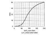
図9はルックアップテーブルLUT_G2VV25において記憶される、横軸を6ビットの階調値、縦軸を正規化された印加電圧Veの自乗値Ve^2(8ビット値)としてプロットした関係を示すグラフであり、図10はルックアップテーブルLUT_VV2G27はルックアップテーブルLUT_G2VV25の縦軸と横軸を交換してプロットしたものである。いずれも一次元のルックアップテーブルである。 FIG. 9 is a graph showing the relationship stored in the look-up table LUT_G2VV25, plotted with the horizontal axis representing 6-bit gradation values and the vertical axis representing the squared value Ve ^ 2 (8-bit value) of the normalized applied voltage Ve. In FIG. 10, the lookup table LUT_VV2G27 is plotted by exchanging the vertical axis and the horizontal axis of the lookup table LUT_G2VV25. Both are one-dimensional lookup tables.
次にこれらのルックアップテーブルを用いる図3の構成における動作を図11を参照して説明する。 Next, the operation in the configuration of FIG. 3 using these lookup tables will be described with reference to FIG.
スタート階調値Gn-1およびエンド階調値Gnが入力されると、比較器21においてこれらが同じ値であるか否かが比較され(ステップS101)、同じである場合(場合0)のときは、オーバードライブ値ODをGn、予測階調値PDをGnとして出力する(ステップS111)。
When the start gradation value Gn-1 and the end gradation value Gn are input, the
スタート階調値Gn-1とエンド階調値Gnとが異なる場合、演算器23においてルックアップテーブルLUT_G2Vs24およびLUT_G2VV25を参照してVVod=LUT_G2Vs(Gn)− LUT_G2Vs(Gn-1)+LUT_G2VV(Gn)を演算し(ステップS102)、VVodは比較器26に与えられると共に選択器/データ発生器22に送られる。
When the start gradation value Gn-1 and the end gradation value Gn are different, the
ここでVVodとは、要求されるオーバードライブ値を正規化された液晶印加電圧の2乗値で表現した値である。 Here, VVod is a value representing a required overdrive value as a square value of a normalized liquid crystal applied voltage.
比較器26では、VVodの値とVVの最大値(MaxVV)および最小値MinVVとが比較され(ステップS103)、MaxVVよりも大きいときには飽和最大オーバードライブを表す場合Aとして、オーパドライブ値ODを63、予測階調値PDはGn-1とオーバードライブ値63に対する値をルックアップテーブルLUT_Predictから取り出して出力する(ステップS112)。一方、MinVVよりも小さいときには飽和最小オーバードライブを表す場合Bとして、オーバードライブ値ODを0、予測階調値PDはGn-1とオーバードライブ値0に対する値をルックアップテーブルLUT_Predictから取り出して出力する(ステップS113)。
In the
VVodの値がVVの最大値(MaxVV)と最小値MinVVとの間にあるときには、適度なオーバードライブを表す場合Cとして、オーバードライブ値ODをルックアップテーブルLUT_VV2G27を参照しVVodに対応する階調値として取り出し、予測値PDをGnとして出力する(ステップS114)。 When the value of VVod is between the maximum value (MaxVV) and the minimum value MinVV of VV, the overdrive value OD is referred to the look-up table LUT_VV2G27 as C when representing an appropriate overdrive, and the gradation corresponding to VVod It takes out as a value and outputs the predicted value PD as Gn (step S114).
この実施例では、参照するLUTはいずれも一次元のものであり、LUTの容量を小さくできるとともに、精度の高い制御が可能となる。 In this embodiment, all the LUTs to be referred to are one-dimensional, and the capacity of the LUT can be reduced and high-precision control is possible.
本発明の第2の実施例を図12から図18までを参照して説明する。 A second embodiment of the present invention will be described with reference to FIGS.
図12は図2に示されたオーバードライブ/予測演算装置の第2実施例の構成を示すブロック図である。 FIG. 12 is a block diagram showing the configuration of the second embodiment of the overdrive / predictive arithmetic unit shown in FIG.
図3に示した第1の実施例と構成上類似するので、同じ構成要素については説明を省略する。 Since the configuration is similar to that of the first embodiment shown in FIG. 3, the description of the same components is omitted.
図3との相違点は、演算器23が出力VVodを発生させるために参照するルックアップテーブルとしてLUT_G2Vs24に代わるLUT_G2VsVe31とLUT_G2VV25が用いられ、選択器/データ発生器22がオーバードライブ値ODおよび予測値PDを発生させるために参照するルックアップテーブルとしてLUT_VV2G27とLUT_Predict28に代わるLUT_G2VsVe2G32となっている点である。
The difference from FIG. 3 is that LUT_G2VsVe31 and LUT_G2VV25 are used instead of LUT_G2Vs24 as a lookup table to be referred to by the
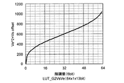
LUT_G2VsVe31の記憶内容を図13に、LUT_VsVe2G32の記憶内容を図14に示す。 FIG. 13 shows the stored contents of LUT_G2VsVe31, and FIG. 14 shows the stored contents of LUT_VsVe2G32.
LUT_G2VsVe31の横軸は0から63までの階調値となっているが、縦軸はオフセットされた印加電圧VsoffsetにVe^2の値を加えたものとなっており、そのサイズは64×1×13ビットとなっている。 The horizontal axis of LUT_G2VsVe31 is the gradation value from 0 to 63, but the vertical axis is the offset applied voltage Vsoffset plus the value of Ve ^ 2, and its size is 64 × 1 × It is 13 bits.
すなわち、LUT_G2VsVe = LUT_G2VV + LUT_G2Vs
の関係が成立する。
That is, LUT_G2VsVe = LUT_G2VV + LUT_G2Vs
The relationship is established.
図14に示すルックアップテーブルLUT_VsVe2G32は、図13に示すLUT_G2VsVe31の縦軸と横軸を交換したものであり、そのサイズは8192(13ビットに相当)×1×6ビットとなっている。なお、13ビットは−30度までの動作温度範囲を考慮した場合であって、よりせまい(高温側の)動作温度範囲のみを考える場合は、より少ないビット数であってもよい。 The look-up table LUT_VsVe2G32 shown in FIG. 14 is obtained by exchanging the vertical axis and the horizontal axis of the LUT_G2VsVe31 shown in FIG. 13 and has a size of 8192 (corresponding to 13 bits) × 1 × 6 bits. Note that 13 bits is a case where an operating temperature range up to −30 degrees is considered, and when only a narrower (higher temperature side) operating temperature range is considered, the number of bits may be smaller.
図15は第1の実施例における図11と対応する、図12の構成における動作を示すフローチャートである。 FIG. 15 is a flowchart showing the operation of the configuration of FIG. 12 corresponding to FIG. 11 in the first embodiment.
スタート階調値Gn-1およびエンド階調値Gnが入力されると、比較器21においてこれらが同じ値であるか否かが比較され(ステップS201)、同じである場合(場合0)のときは、オーバードライブ値ODをGn、予測階調値PDをGnとして出力する(ステップS211)。
When the start gradation value Gn-1 and the end gradation value Gn are input, the
スタート階調値Gn-1とエンド階調値Gnとが異なる場合、演算器23においてルックアップテーブルLUT_G2VsVe31およびLUT_G2VV25を参照してまず
Vs(Gn-1)=LUT_G2VsVe(Gn-1)− LUT_G2VV(Gn-1)
として求める。次に、
VVod=LUT_G2VsVe(Gn)− Vs(Gn-1)
として求め、これら両方は選択器/データ発生器22に供給されるが、比較器26にはVVodのみが送られる(ステップS202)。
When the start gradation value Gn-1 and the end gradation value Gn are different, the
Vs (Gn-1) = LUT_G2VsVe (Gn-1)-LUT_G2VV (Gn-1)
Asking. next,
VVod = LUT_G2VsVe (Gn)-Vs (Gn-1)
Both are supplied to the selector /
比較器26では、VVodの値とVVの最大値(MaxVV)および最小値MinVVとが比較され(ステップS203)、MaxVVよりも大きいときには飽和最大オーバードライブを表す場合Aとして、オーバードライブ値を63、予測階調値PDはLUT_VsVe2G(LUT_G2VV(63)+Vs(Gn-1)として出力される(ステップS212)。
In the
一方、VVodの値がMinVVよりも小さいときには飽和最小オーバードライブを表す場合Bとして、オーバードライブ値を0、予測階調値PDはLUT_VsVe2G(LUT_G2VV(0)+Vs(Gn-1)として出力される(ステップS213)。 On the other hand, when the value of VVod is smaller than MinVV, the overdrive value is 0 as the saturation minimum overdrive, and the predicted gradation value PD is output as LUT_VsVe2G (LUT_G2VV (0) + Vs (Gn-1)). Step S213).
VVodの値がVVの最大値(MaxVV)と最小値MinVVとの間にあるときには、適度なオーバードライブを表す場合Cとして、オーバードライブ値ODをルックアップテーブルLUT_VV2G(VVod)により階調値に変換した値とし、予測値PDをGnとして出力する(ステップS214)。 When the value of VVod is between the maximum value (MaxVV) and the minimum value MinVV of VV, the overdrive value OD is converted into a gradation value by the lookup table LUT_VV2G (VVod) as C when representing an appropriate overdrive. The predicted value PD is output as Gn (step S214).
この実施例でも、参照するLUTはいずれも一次元のものであり、LUTの容量を小さくできるとともに、精度の高い制御が可能となる。 Also in this embodiment, the LUTs to be referred to are one-dimensional, and the capacity of the LUT can be reduced, and high-precision control is possible.
図16から図18はVsoffset、正規化されたエンド電圧Veの2乗値Ve^2(=VV)、これらの合計の値Ve^2 +Vsoffset(=VsVe)を表す3つの曲線を用いてスタート値Gn-1、エンド値Gn、オーバードライブ値God、予測値Gpredictを求める手順を示す説明図である。ここで記号のVは電圧に基づく値、Gは階調の値を意味する。 16 to 18 start with three curves representing Vsoffset, the squared value Ve ^ 2 (= VV) of the normalized end voltage Ve, and the total value Ve ^ 2 + Vsoffset (= VsVe). It is explanatory drawing which shows the procedure which calculates | requires value Gn-1, end value Gn, overdrive value God, and predicted value Gpredict. Here, the symbol V means a value based on voltage, and G means a gradation value.
前述したように、VsoffsetはルックアップテーブルLUT_G2Vs24の記憶内容であり、Ve^2はルックアップテーブルLUT_G2VV25の記憶内容であり、Ve^2 +VsoffsetはルックアップテーブルLUT_G2VsVe31の記憶内容となっている。 As described above, Vsoffset is the storage content of the lookup table LUT_G2Vs24, Ve ^ 2 is the storage content of the lookup table LUT_G2VV25, and Ve ^ 2 + Vsoffset is the storage content of the lookup table LUT_G2VsVe31.
図16は、スタート階調値Gn-1およびエンド階調値Gnが同じ場合を示している。(Gn=Gn-1=32)
この場合には、図11および図15からオーバードライブ値ODはGn、予測階調値PDもGnであるから、
Gn-1=Gn=God=Gpredict
であり、各曲線の縦軸の値を参照することなくGod=Gpredict=32と決定される。
FIG. 16 shows a case where the start gradation value Gn−1 and the end gradation value Gn are the same. (Gn = Gn-1 = 32)
In this case, since the overdrive value OD is Gn and the predicted gradation value PD is Gn from FIGS.
Gn-1 = Gn = God = Gpredict
Therefore, God = Gpredict = 32 is determined without referring to the value on the vertical axis of each curve.
なお、この場合は、ルックアップテーブルLUT_G2VsVe31の記憶内容を定義する。すなわち、各階調に対するVsoffsetの値と、Ve^2の値を合計した値が同じ階調値に対するVe^2 +Vsoffset上の値となっている。 In this case, the stored contents of the lookup table LUT_G2VsVe31 are defined. That is, the value of Vsoffset for each gradation and the sum of the values of Ve ^ 2 are values on Ve ^ 2 + Vsoffset for the same gradation value.
図16においては、階調値32に対し、ルックアップテーブルLUT_G2Vs24から取り出された値54とルックアップテーブルLUT_G2VV25から取り出された値117の合計値171がルックアップテーブルLUT_G2VsVe31の階調値32に対する値となり、以下、各階調値毎に2つのルックアップテーブルを参照することによりルックアップテーブルLUT_G2VsVe31を作成できる。
LUT_G2VsVe(x) = LUT_G2Vs(x) + LUT_G2VV(x);ここでxは任意の階調値0〜63
そして、このルックアップテーブルが作成された後はVsoffsetの値は2つのルックアップテーブルLUT_G2VsVe31とLUT_G2VV25により求めることができるので、図12のように、ルックアップテーブルLUT_G2Vs24は不要となる。
In FIG. 16, the total value 171 of the
LUT_G2VsVe (x) = LUT_G2Vs (x) + LUT_G2VV (x); where x is an
After the lookup table is created, the value of Vsoffset can be obtained from the two lookup tables LUT_G2VsVe31 and LUT_G2VV25, so that the lookup table LUT_G2Vs24 becomes unnecessary as shown in FIG.
図17は、スタート階調値Gn-1およびエンド階調値Gnが適度に離れている場合を示し、スタート階調値Gn-1が8、エンド階調値Gnが32の場合を示している。これは図11、図15における場合C;適度なODの例である。 FIG. 17 shows a case where the start gradation value Gn−1 and the end gradation value Gn are appropriately separated, and shows a case where the start gradation value Gn−1 is 8 and the end gradation value Gn is 32. . This is an example of an appropriate OD in FIG. 11 and FIG.
まず曲線Ve^2+Vsoffset上のポイント(32、171)を参照されたい。このポイントのエンド階調Gn=32を得るためには、Ve^2+Vsoffset=171が必要である。次に曲線Vsoffset上のポイント(8、26)を見ると、スタート階調Gn-1=8に対するVsoffsetは26であることがわかる。よって、オーバードライブに必要なVe^2の値は残り171−26=145(=VVod)である。これを曲線Ve^2上で参照すると、ポイント(44、145)になる。つまりオーバードライブ階調値Godは44である。なお、予測階調値はエンド階調に等しくなるので、Gpredict=Gn=32である。 First, refer to the points (32, 171) on the curve Ve ^ 2 + Vsoffset. In order to obtain the end gradation Gn = 32 at this point, Ve ^ 2 + Vsoffset = 171 is necessary. Next, looking at the points (8, 26) on the curve Vsoffset, it can be seen that the Vsoffset for the start gradation Gn−1 = 8 is 26. Therefore, the value of Ve ^ 2 necessary for overdrive is the remaining 171-26 = 145 (= VVod). If this is referred to on the curve Ve ^ 2, it becomes a point (44, 145). That is, the overdrive tone value God is 44. Since the predicted gradation value is equal to the end gradation, Gpredict = Gn = 32.
さらに、これらの事を図16との対比で説明する。まずスタート階調Gn-1は32から8に変わっていることから、Vsoffsetは54から26へと、−28変化している。この分をVe^2で補償するには、Ve^2を+28する必要がある。つまりVe^2=117+28=145とすればよい。このとき階調値44がGodとなる。このようにして、Ve^2+Vsoffsetが一定値を保つようにバランスをとることで、同じエンド階調値Gnを達成できる。
Further, these will be described in comparison with FIG. First, since the start gradation Gn-1 is changed from 32 to 8, Vsoffset is changed by -28 from 54 to 26. To compensate this amount with Ve ^ 2, Ve ^ 2 needs to be +28. That is, Ve ^ 2 = 117 + 28 = 145. At this time, the
このように、適度なODの例では予測階調値は計算によって求める必要が無く、常にGpredict=Gnである。 Thus, in an example of a moderate OD, the predicted gradation value does not need to be obtained by calculation, and Gpredict = Gn is always established.
図18は最大オーバードライブの場合であり、スタート階調値Gn-1が0、エンド階調値Gnが60の場合を示している。これは図11、図15における場合Aの例である。 FIG. 18 shows the case of maximum overdrive, in which the start gradation value Gn-1 is 0 and the end gradation value Gn is 60. This is an example of case A in FIGS.
まず曲線Ve^2+Vsoffset上のポイント(60、301)を参照されたい。このポイントのエンド階調Gn=60を得るためには、Ve^2+Vsoffset=301が必要である。これに対して、曲線Vsoffset上のポイント(0,0)を見ると、スタート階調Gn-1=0に対するVsoffsetは0であることがわかる。よって、オーバードライブに必要なVe^2の値は残り301−0=301(=VVod)である。しかしながら、曲線Ve^2上のポイント(63、255)を参照すると、Ve^2の最大値(maxVV)は、God=63のときに255である。つまり、残り301−255=46は最大オーバードライブでも補償できないことになる(VVod > maxVV)。この場合、最大オーバードライブGodとして63を出力し、予測階調値Gpredictは、曲線Ve^2+Vsoffset上で、Ve^2+Vsoffset=0+255=255となる点を見ると、54とわかる。(Gpredict≠Gn) First, see the point (60, 301) on the curve Ve ^ 2 + Vsoffset. In order to obtain the end gradation Gn = 60 at this point, Ve ^ 2 + Vsoffset = 301 is necessary. On the other hand, when the point (0, 0) on the curve Vsoffset is seen, it can be seen that Vsoffset for the start gradation Gn−1 = 0 is zero. Therefore, the value of Ve ^ 2 necessary for overdrive is the remaining 301-0 = 301 (= VVod). However, referring to the point (63, 255) on the curve Ve ^ 2, the maximum value of Ve ^ 2 (maxVV) is 255 when God = 63. That is, the remaining 301-255 = 46 cannot be compensated even by the maximum overdrive (VVod> maxVV). In this case, 63 is output as the maximum overdrive God, and the predicted gradation value Gpredict is 54 when it is seen on the curve Ve ^ 2 + Vsoffset that Ve ^ 2 + Vsoffset = 0 + 255 = 255. (Gpredict ≠ Gn)
また、これらの事をGn=Gn-1=60であった場合との対比で説明する。まずスタート階調Gn-1は60から0に変わっていることから、Vsoffsetは77から0へと、−77変化している。この分をVe^2つまりオーバードライブで補償する必要がある。よってVe^2を224から301へと+77とすればよい。しかしながら、Ve^2の最大値(maxVV)は255であるから、実際の補償は255−224=+31と十分でなく、エンド階調値Gnを達成することはできない。 These will be described in comparison with the case where Gn = Gn-1 = 60. First, since the start gradation Gn-1 has changed from 60 to 0, Vsoffset has changed by 77 from 77 to 0. It is necessary to compensate for this by Ve ^ 2, that is, overdrive. Therefore, Ve ^ 2 should be +77 from 224 to 301. However, since the maximum value (maxVV) of Ve ^ 2 is 255, the actual compensation is not sufficient as 255−224 = + 31, and the end gradation value Gn cannot be achieved.
これまでの図16から図18の説明で行われた計算を、あらためてルックアップテーブルを用いた計算式で示す。
VVod = LUT_G2VsVe(Gn)−LUT_G2Vs(Gn-1) ・・・・・・・・・・実施例2
= LUT_G2Vs(Gn)+LUT_G2VV(Gn)−LUT_G2Vs(Gn-1) ・・・実施例1
ここで、実施例2から1への式変形は、前述の関係式を代入することでなされる。
OD=LUT_VV2G(VVod) (0<VVod<255のとき)
=63 (VVod>255のとき)
=0 (VVod<0のとき)
PD=LUT_VsVe2G(LUT_G2Vs(Gn-1)+LUT_G2VV(VVod))
=LUT_VsVe2G(LUT_G2VsVe(Gn-1)−LUT_G2VV(Gn-1)+LUT_G2VV(VVod)) ・・・実施例2
The calculations performed so far in the description of FIGS. 16 to 18 are shown again by calculation formulas using a lookup table.
VVod = LUT_G2VsVe (Gn) −LUT_G2Vs (Gn−1) ・ ・ ・ ・ ・ ・ ・ ・ ・ ・ Example 2
= LUT_G2Vs (Gn) + LUT_G2VV (Gn) −LUT_G2Vs (Gn−1)... Example 1
Here, the transformation from the second embodiment to the first embodiment is performed by substituting the above-described relational expression.
OD = LUT_VV2G (VVod) (when 0 <VVod <255)
= 63 (when VVod> 255)
= 0 (when VVod <0)
PD = LUT_VsVe2G (LUT_G2Vs (Gn-1) + LUT_G2VV (VVod))
= LUT_VsVe2G (LUT_G2VsVe (Gn-1) -LUT_G2VV (Gn-1) + LUT_G2VV (VVod))) ... Example 2
上記の式変形にも前述の関係式を用いた。さらに、PDはGn-1とVVodの2変数で決まるといえるが、VVodが0から255の範囲内では予測階調値はエンド階調に一致する(PD=Gn)ので計算により求める必要が無い。そこでVVod=0とVVod=255のときの予測階調値のみをあらかじめ計算により求めておけば、2本の一次元ルックアップテーブルとして計算を簡略化できる。すなわち、
PD=LUT_predict(Gn-1, OD0/OD255) ・・・実施例1
The above-described relational expression was also used for the above-described expression modification. Furthermore, although it can be said that PD is determined by two variables of Gn-1 and VVod, when VVod is in the range of 0 to 255, the predicted gradation value matches the end gradation (PD = Gn), so there is no need to obtain it by calculation. . Therefore, if only the predicted gradation values when VVod = 0 and VVod = 255 are obtained in advance, the calculation can be simplified as two one-dimensional lookup tables. That is,
PD = LUT_predict (Gn-1, OD0 / OD255) ... Example 1
このように、電圧値の2乗を座標値にしたルックアップテーブルを採用することにより、装置の構成が簡単になり、演算が容易になる。 In this way, by employing a lookup table in which the square of the voltage value is a coordinate value, the configuration of the apparatus is simplified and the calculation is facilitated.
なお、液晶の温度特性は温度で劇的に変わるため、実施例では5℃刻で設けられていたものとしたが、メモリ容量が削減された分をルックアップテーブルの温度の刻みを細かくすることに振り分けることもできる。 Since the temperature characteristics of the liquid crystal change dramatically depending on the temperature, it was assumed that the liquid crystal was provided at 5 ° C. in the example. However, the amount of memory capacity is reduced, and the temperature increment of the lookup table is reduced. You can also sort them into
以上の説明は一例であって、当業者が通常行う変形、置換などは本発明の範囲である。 The above description is merely an example, and modifications, replacements, and the like normally performed by those skilled in the art are within the scope of the present invention.
以上説明した本発明にかかる液晶表示装置は、携帯電話、デジタルカメラ、PDA(パーソナルデジタルアシスタント)、自動車用ディスプレイ、航空用ディスプレイ、デジタルフォトフレーム、またはポータブルDVDプレーヤなどの各種電子装置に使用することができ、特に低温環境で用いるものに好適である。 The liquid crystal display device according to the present invention described above is used for various electronic devices such as a mobile phone, a digital camera, a PDA (personal digital assistant), an automobile display, an aircraft display, a digital photo frame, or a portable DVD player. It is particularly suitable for use in a low temperature environment.
10 液晶パネル
11 行デコーダ
12 列デコーダ
13 電圧変換部
14 温度センサ
15 フレームメモリ
20 オーバードライブ/予測演算装置
21 比較器
22 選択器
23 演算器
24 ルックアップテーブルLUT_G2Vs
25 ルックアップテーブルLUT_G2VV
26 選択器/データ発生器22
27 ルックアップテーブルLUT_VV2G
28 ルックアップテーブルLUT_Predict
29 遅延器
30 遅延器
31 ルックアップテーブルLUT_G2VsVe
32 ルックアップテーブルLUT_VsVe2G
DESCRIPTION OF
25 Lookup table LUT_G2VV
26 Selector /
27 Lookup table LUT_VV2G
28 Lookup table LUT_Predict
29
32 Lookup table LUT_VsVe2G
Claims (4)
前記液晶表示モジュール中に設けられた温度センサと、
イメージデータ中のスタート階調値とエンド階調値から、前記液晶表示モジュールに対するオーバードライブ電圧と次フレームに対する予測値を演算し出力する演算装置と、
前記予測値を記憶し、前記スタート階調値として前記演算装置に対して出力するフレームメモリとを備え、
前記演算装置は、
前記スタート階調値と前記エンド階調値が一致するか否かを検知する第1の比較器と、
階調値と、階調値に応じる電圧の2乗値で構成される曲線が一致するように正規化されたオフセット量との関係を表す一次元の第1のルックアップテーブルと、
階調値と、階調値に応じる電圧の2乗値との関係を表す一次元の第2のルックアップテーブルと、
前記スタート階調値と前記エンド階調値と、前記第1および第2のルックアップテーブルの値を参照して、前記電圧の2乗値に関連したオーバードライブ用の中間出力値を求める演算器と、
前記演算器の出力が所定の最大値より大きいか、所定の最小値より小さいか、中間値かを判断する第2の比較器と、
前記第1および第2の比較器の出力に応じて参照されるオーバードライブ値算出のための一次元の第3のルックアップテーブルと、
前記第1および第2の比較器の出力に応じて参照される予測値算出のための一次元の第4のルックアップテーブルとを備え、
前記第1〜4のルックアップテーブルは前記温度センサの値に応じて随時更新され、
前記第1の比較器、前記第2の比較器、前記演算器の出力を用いて、前記スタート階調値とエンド階調値が一致する第1の場合、前記階調差が前記所定の最大値よりも大きい第2の場合、前記階調差が前記所定の最小値よりも小さい第3の場合、前記階調差が前記所定の最大値と最小値の間にある第4の場合の4つの場合に応じてオーバードライブ出力および予測出力を発生する選択器/データ発生器とを備えたことを特徴とする液晶表示装置。 A liquid crystal display module;
A temperature sensor provided in the liquid crystal display module;
An arithmetic device that calculates and outputs an overdrive voltage for the liquid crystal display module and a predicted value for the next frame from a start gradation value and an end gradation value in image data;
A frame memory that stores the prediction value and outputs the start gradation value to the arithmetic unit;
The arithmetic unit is:
A first comparator for detecting whether the start gradation value and the end gradation value match;
A first one-dimensional lookup table representing a relationship between a gradation value and an offset amount normalized so that a curve formed by a square value of a voltage corresponding to the gradation value matches;
A one-dimensional second look-up table representing a relationship between a gradation value and a square value of a voltage corresponding to the gradation value;
An arithmetic unit for obtaining an intermediate output value for overdrive related to the square value of the voltage with reference to the start gradation value, the end gradation value, and the values of the first and second lookup tables When,
A second comparator for determining whether the output of the computing unit is greater than a predetermined maximum value, less than a predetermined minimum value, or an intermediate value;
A one-dimensional third look-up table for calculating an overdrive value referred to according to the outputs of the first and second comparators;
A one-dimensional fourth look-up table for calculating a predicted value referred to according to the outputs of the first and second comparators,
The first to fourth look-up tables are updated as needed according to the value of the temperature sensor,
In the first case where the start gradation value and the end gradation value coincide with each other using the outputs of the first comparator, the second comparator, and the arithmetic unit, the gradation difference is the predetermined maximum. 4 in the fourth case where the gradation difference is between the predetermined maximum value and the minimum value in the second case where the gradation difference is smaller than the predetermined minimum value. A liquid crystal display device comprising a selector / data generator for generating an overdrive output and a predicted output according to one case.
第3のルックアップテーブルが正規化された液晶印加電圧の2乗値に対する階調値を記憶したものであることを特徴とする請求項1に記載の液晶表示装置。 The second lookup table stores the normalized squared value of the liquid crystal applied voltage with respect to the gradation value;
2. The liquid crystal display device according to claim 1, wherein the third look-up table stores a gradation value with respect to a square value of the normalized liquid crystal applied voltage.
第4のルックアップテープルはこの第1のルックアップテーブルの横座標と縦座標を交換したものである、請求項1または2に記載の液晶表示装置。 The first look-up table is obtained by adding the square value of the voltage defined by the second look-up table to the normalized offset amount with respect to the gradation value,
The liquid crystal display device according to claim 1 or 2, wherein the fourth look-up table is obtained by exchanging the abscissa and ordinate of the first look-up table.
Priority Applications (3)
| Application Number | Priority Date | Filing Date | Title |
|---|---|---|---|
| TW98139139A TWI412013B (en) | 2008-11-28 | 2009-11-18 | Liquid crystal display |
| CN2009102463632A CN101751892B (en) | 2008-11-28 | 2009-11-27 | Liquid crystal display device |
| US12/627,177 US8144105B2 (en) | 2008-11-28 | 2009-11-30 | LCD with adaptive overdrive |
Applications Claiming Priority (2)
| Application Number | Priority Date | Filing Date | Title |
|---|---|---|---|
| US11850808P | 2008-11-28 | 2008-11-28 | |
| US61/118,508 | 2008-11-28 |
Publications (2)
| Publication Number | Publication Date |
|---|---|
| JP2010128497A JP2010128497A (en) | 2010-06-10 |
| JP4982760B2 true JP4982760B2 (en) | 2012-07-25 |
Family
ID=42328891
Family Applications (1)
| Application Number | Title | Priority Date | Filing Date |
|---|---|---|---|
| JP2009180956A Expired - Fee Related JP4982760B2 (en) | 2008-11-28 | 2009-08-03 | Liquid crystal display |
Country Status (3)
| Country | Link |
|---|---|
| JP (1) | JP4982760B2 (en) |
| CN (1) | CN101751892B (en) |
| TW (1) | TWI412013B (en) |
Families Citing this family (5)
| Publication number | Priority date | Publication date | Assignee | Title |
|---|---|---|---|---|
| KR20120089081A (en) | 2011-02-01 | 2012-08-09 | 삼성전자주식회사 | Liquid crystal display, device and method of modifying image signal |
| US9224340B2 (en) * | 2012-05-23 | 2015-12-29 | Dialog Semiconductor Inc. | Predictive power control in a flat panel display |
| DE102014210834B3 (en) * | 2014-06-06 | 2015-09-03 | Robert Bosch Gmbh | Method for the control of a display device and display device for a particular motor vehicle |
| KR20200000857A (en) * | 2018-06-25 | 2020-01-06 | 삼성디스플레이 주식회사 | Liquid crystal display device and method driving for the same |
| KR102602068B1 (en) * | 2018-10-30 | 2023-11-15 | 삼성디스플레이 주식회사 | Display apparatus and method of driving display apparatus using the same |
Family Cites Families (5)
| Publication number | Priority date | Publication date | Assignee | Title |
|---|---|---|---|---|
| US8049691B2 (en) * | 2003-09-30 | 2011-11-01 | Sharp Laboratories Of America, Inc. | System for displaying images on a display |
| JP4341839B2 (en) * | 2003-11-17 | 2009-10-14 | シャープ株式会社 | Image display device, electronic apparatus, liquid crystal television device, liquid crystal monitor device, image display method, display control program, and recording medium |
| KR101056371B1 (en) * | 2004-09-08 | 2011-08-11 | 삼성전자주식회사 | Display device, driving method and device thereof |
| CN100353412C (en) * | 2005-06-03 | 2007-12-05 | 友达光电股份有限公司 | Pixel driving method, timing controller and flat panel display |
| JP2008250222A (en) * | 2007-03-30 | 2008-10-16 | Casio Comput Co Ltd | Liquid crystal drive device and liquid crystal display device |
-
2009
- 2009-08-03 JP JP2009180956A patent/JP4982760B2/en not_active Expired - Fee Related
- 2009-11-18 TW TW98139139A patent/TWI412013B/en not_active IP Right Cessation
- 2009-11-27 CN CN2009102463632A patent/CN101751892B/en active Active
Also Published As
| Publication number | Publication date |
|---|---|
| JP2010128497A (en) | 2010-06-10 |
| TW201023165A (en) | 2010-06-16 |
| TWI412013B (en) | 2013-10-11 |
| CN101751892A (en) | 2010-06-23 |
| CN101751892B (en) | 2012-09-26 |
Similar Documents
| Publication | Publication Date | Title |
|---|---|---|
| JP4560567B2 (en) | Overdrive method for liquid crystal display device and liquid crystal display device | |
| CN100511402C (en) | Methods, circuits and displays for selectively compensating for gray-scale | |
| JP4779167B2 (en) | Method for driving liquid crystal display device, overdrive correction device, data creation method for overdrive correction device, liquid crystal display device, and electronic device | |
| US20060158415A1 (en) | Overdrive circuit having a temperature coefficient look-up table and liquid crystal display panel driving apparatus including the same | |
| US20020033789A1 (en) | Liquid crystal display device and driving method thereof | |
| TW200305844A (en) | Liquid crystal display | |
| JPWO2003098588A1 (en) | Liquid crystal display device | |
| KR20040053640A (en) | Driving apparatus of liquid crystal display for varying limits selecting gray voltages and method thereof | |
| JP4982760B2 (en) | Liquid crystal display | |
| JP5354927B2 (en) | Liquid crystal display | |
| CN101083065A (en) | Liquid crystal display device and driving method thereof | |
| US8144105B2 (en) | LCD with adaptive overdrive | |
| CN109326252B (en) | Display driver, display controller, electro-optical device, and electronic apparatus | |
| CN101501752B (en) | Liquid crystal panel drive device, liquid crystal panel drive method, liquid crystal display device, vehicle-mounted display device | |
| JP2019028292A (en) | Display driver, display controller, electro-optic device, and electronic apparatus | |
| US20080297497A1 (en) | Control circuit and method of liquid crystal display panel | |
| JP2019095527A (en) | Display driver, display device, and image correction method | |
| KR101437869B1 (en) | Data processing apparatus, liquid crystal display comprising the same and control method thereof | |
| JP2015197476A (en) | Signal processing method, display device, and electronic apparatus | |
| KR102252817B1 (en) | Method of driving display panel and display apparatus of performing the same | |
| KR100686680B1 (en) | LCD and its processing method | |
| KR20070019405A (en) | Liquid Crystal Display and Image Signal Correction Method | |
| CN100390620C (en) | Liquid crystal display and its driving method | |
| JP2003084741A (en) | Method and apparatus for driving liquid crystal display device | |
| US20070159431A1 (en) | Liquid crystal display device and liquid crystal driver |
Legal Events
| Date | Code | Title | Description |
|---|---|---|---|
| TRDD | Decision of grant or rejection written | ||
| A01 | Written decision to grant a patent or to grant a registration (utility model) |
Free format text: JAPANESE INTERMEDIATE CODE: A01 Effective date: 20120302 |
|
| A01 | Written decision to grant a patent or to grant a registration (utility model) |
Free format text: JAPANESE INTERMEDIATE CODE: A01 |
|
| A711 | Notification of change in applicant |
Free format text: JAPANESE INTERMEDIATE CODE: A712 Effective date: 20120329 |
|
| A61 | First payment of annual fees (during grant procedure) |
Free format text: JAPANESE INTERMEDIATE CODE: A61 Effective date: 20120329 |
|
| R150 | Certificate of patent or registration of utility model |
Free format text: JAPANESE INTERMEDIATE CODE: R150 Ref document number: 4982760 Country of ref document: JP Free format text: JAPANESE INTERMEDIATE CODE: R150 |
|
| FPAY | Renewal fee payment (event date is renewal date of database) |
Free format text: PAYMENT UNTIL: 20150511 Year of fee payment: 3 |
|
| FPAY | Renewal fee payment (event date is renewal date of database) |
Free format text: PAYMENT UNTIL: 20150511 Year of fee payment: 3 |
|
| R154 | Certificate of patent or utility model (reissue) |
Free format text: JAPANESE INTERMEDIATE CODE: R154 |
|
| R250 | Receipt of annual fees |
Free format text: JAPANESE INTERMEDIATE CODE: R250 |
|
| R250 | Receipt of annual fees |
Free format text: JAPANESE INTERMEDIATE CODE: R250 |
|
| R250 | Receipt of annual fees |
Free format text: JAPANESE INTERMEDIATE CODE: R250 |
|
| R250 | Receipt of annual fees |
Free format text: JAPANESE INTERMEDIATE CODE: R250 |
|
| R250 | Receipt of annual fees |
Free format text: JAPANESE INTERMEDIATE CODE: R250 |
|
| R250 | Receipt of annual fees |
Free format text: JAPANESE INTERMEDIATE CODE: R250 |
|
| LAPS | Cancellation because of no payment of annual fees |