JP4982932B2 - Manufacturing method of image display device - Google Patents
Manufacturing method of image display device Download PDFInfo
- Publication number
- JP4982932B2 JP4982932B2 JP2001265595A JP2001265595A JP4982932B2 JP 4982932 B2 JP4982932 B2 JP 4982932B2 JP 2001265595 A JP2001265595 A JP 2001265595A JP 2001265595 A JP2001265595 A JP 2001265595A JP 4982932 B2 JP4982932 B2 JP 4982932B2
- Authority
- JP
- Japan
- Prior art keywords
- resin
- light
- light emitting
- wiring
- substrate
- Prior art date
- Legal status (The legal status is an assumption and is not a legal conclusion. Google has not performed a legal analysis and makes no representation as to the accuracy of the status listed.)
- Expired - Fee Related
Links
Images






Classifications
-
- H—ELECTRICITY
- H10—SEMICONDUCTOR DEVICES; ELECTRIC SOLID-STATE DEVICES NOT OTHERWISE PROVIDED FOR
- H10W—GENERIC PACKAGES, INTERCONNECTIONS, CONNECTORS OR OTHER CONSTRUCTIONAL DETAILS OF DEVICES COVERED BY CLASS H10
- H10W70/00—Package substrates; Interposers; Redistribution layers [RDL]
- H10W70/60—Insulating or insulated package substrates; Interposers; Redistribution layers
-
- H—ELECTRICITY
- H10—SEMICONDUCTOR DEVICES; ELECTRIC SOLID-STATE DEVICES NOT OTHERWISE PROVIDED FOR
- H10W—GENERIC PACKAGES, INTERCONNECTIONS, CONNECTORS OR OTHER CONSTRUCTIONAL DETAILS OF DEVICES COVERED BY CLASS H10
- H10W90/00—Package configurations
- H10W90/10—Configurations of laterally-adjacent chips
Landscapes
- Electrodes Of Semiconductors (AREA)
- Internal Circuitry In Semiconductor Integrated Circuit Devices (AREA)
- Die Bonding (AREA)
- Led Device Packages (AREA)
Abstract
Description
【0001】
【発明の属する技術分野】
本発明は、樹脂層に形成される配線や接続孔、その形成方法に関するものであり、さらには、その配線形成体及びその形成方法に関するものである。また、本発明は、これを応用した表示素子及びその形成方法、画像表示装置及びその製造方法に関するものである。
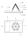
【0002】
【従来の技術】
例えば、発光素子をマトリクス状に配列して画像表示装置に組み上げる場合には、従来、液晶表示装置(LCD:Liquid Crystal Display)やプラズマディスプレイパネル(PDP:Plasma Display Panel)のように基板上に直接素子を形成するか、あるいは発光ダイオードディスプレイ(LEDディスプレイ)のように単体のLEDパッケージを配列することが行われている。例えば、LCD、PDPの如き画像表示装置においては、素子分離ができないために、製造プロセスの当初から各素子はその画像表示装置の画素ピッチだけ間隔を空けて形成することが通常行われている。
【0003】
一方、LEDディスプレイの場合には、LEDチップをダイシング後に取り出し、個別にワイヤーボンドもしくはフリップチップによるバンプ接続により外部電極に接続し、パッケージ化されることが行われている。この場合、パッケージ化の前もしくは後に画像表示装置としての画素ピッチに配列されるが、この画素ピッチは素子形成時の素子のピッチとは無関係とされる。
【0004】
発光素子であるLED(発光ダイオード)は高価である為、1枚のウエハから数多くのLEDチップを製造することによりLEDを用いた画像表示装置を低コストにできる。すなわち、LEDチップの大きさを従来約300μm角のものを数十μm角のLEDチップにして、それを接続して画像表示装置を製造すれば画像表示装置の価格を下げることができる。
【0005】
【発明が解決しようとする課題】
上述のような転写技術により画像表示装置を製造する場合、効率的な転写、精度の良い転写を実現するために、発光素子をチップ部品化することが好ましい。ここで、発光素子をチップ部品化するには、発光素子を樹脂材料に埋め込み、これを切り出して表示素子として取り扱えばよい。
【0006】
ところで、このように発光素子を樹脂に埋め込んでチップ部品化する場合、樹脂上に発光素子と接続される配線を形成し、これを外部との接続のための電極とする必要がある。従来、樹脂上に金属からなる配線を形成するには、銅メッキなどの方法によるのが一般的である。しかしながら、メッキ法の場合、例えば電解メッキであれば予め電極として機能する層が必要になったり、無電解メッキであれば成膜の制御が困難であるなどの欠点がある。また、全面にメッキ法で成膜した後にパターニングするというプロセスを経る場合には、工程数も多く煩雑であるという問題もある。この点、導電性ペーストを用いた印刷法による場合、成膜と同時にパターニングされるため工程数は少なくすることができるが、例えば下層パターンとの位置合わせ精度の点で問題を残している。
【0007】
本発明は、かかる従来の実情に鑑みて提案されたものであり、工程数を削減することができ、簡単に精度の良い配線形成、接続孔形成が可能な配線及び配線形成方法、接続孔及び接続孔形成方法、さらには配線形成体及びその形成方法を提供することを目的とする。
【0008】
また、本発明は、これを応用した表示素子の形成方法、画像表示装置の製造方法を提供することを目的とする。すなわち、発光素子を樹脂によりモジュール化した場合にも良好な電極形成が可能で、搬送や基体への実装も容易であるような構造を有し信頼性の高い表示素子を作製し得る表示素子の形成方法を提供することを目的とし、さらには、生産性に優れ製造コストを抑えることが可能な画像表示装置の製造方法を提供することを目的とする。
【0009】
【課題を解決するための手段】
上述の目的を達成するために、本発明の配線は、樹脂層に配線パターンに応じて溝が形成されるとともに、上記溝形状に倣って微粒子型導電ペーストが焼結されていることを特徴とするものである。また、本発明の配線形成方法は、樹脂層上に金属配線を形成する配線形成方法において、上記樹脂層に配線パターンに応じて溝を形成し、当該溝以外の部分の樹脂層に対して疎水化処理を施した後、あるいは、上記樹脂層に対して疎水化処理を施し、樹脂層に配線パターンに応じて溝を形成した後、微粒子型導電ペーストを塗布し、これを焼結することで上記溝形状に倣った金属配線を形成することを特徴とするものである。
【0010】
微粒子型導電ペーストは、塗布後、焼結すると体積が1/5〜1/10程度に縮むが、この時、樹脂表面を疎水化処理しておけば、上記微粒子型導電ペーストは疎水化された樹脂表面ではじかれ、溝内にのみ選択的に成膜された形となる。これにより、いわゆる自己整合的に配線パターンが形成されることになる。微粒子型導電ペーストは、非常に微細な金属ナノ粒子を分散してなるものであり、微細配線パターンの形成が可能であり、電気的信頼性も高い。
【0011】
さらに、本発明の接続孔は、樹脂層に接続用の孔が形成されるとともに、この孔内に微粒子型導電ペーストが充填され焼結されていることを特徴とするものである。また、本発明の接続孔の形成方法は、樹脂層上に導電材料が充填された接続孔を形成する接続孔形成方法において、上記樹脂層に接続用の孔を形成し、当該孔以外の部分の樹脂層に対して疎水化処理を施した後、あるいは、上記樹脂層に対して疎水化処理を施し、樹脂層に接続用の孔を形成した後、微粒子型導電ペーストを塗布して上記孔に充填し、これを焼結することを特徴とするものである。
【0012】
微粒子型導電ペーストは、低粘度化が可能であるため、微細な孔にも容易に充填可能である。上記のように、樹脂層に孔を形成し、孔以外の部分の樹脂層に対して疎水化処理を施した後、これを塗布すれば、微粒子型導電ペーストは自己整合的に孔の中に充填され、いわゆるスルーホール(接続孔)が容易に形成される。
【0013】
さらにまた、本発明の配線形成体は、樹脂層に配線パターンに応じて溝が形成されるとともに接続用の孔が形成され、上記溝形状に倣って微粒子型導電ペーストが焼結されるとともに、上記孔に微粒子型導電ペーストが充填され焼結されていることを特徴とするものである。また、本発明の配線形成体の形成方法は、樹脂層に配線パターンに応じて溝を形成するとともに接続用の孔を形成し、当該溝及び孔以外の部分の樹脂層に対して疎水化処理を施した後、あるいは、樹脂層に対して疎水化処理を施し、樹脂層に配線パターンに応じて溝を形成するとともに接続用の孔を形成した後、微粒子型導電ペーストを塗布し、これを焼結することで上記溝形状に倣った金属配線及び上記孔に導電材料が充填された接続孔を形成することを特徴とするものである。この配線形成体及びその形成方法においては、上記配線形成と接続孔形成が同時に自己整合的に行われる。
【0014】
さらにまた、本発明の表示素子は、発光素子が樹脂中に埋め込まれてチップ部品化されるとともに、樹脂表面に溝が形成され、当該溝形状に倣って微粒子型導電ペーストが焼結され電極とされていることを特徴とするものである。また、本発明の表示素子の形成方法は、発光素子を樹脂中に埋め込んでチップ部品化した後、電極を樹脂表面に形成する表示素子の形成方法において、上記樹脂表面に配線パターンに応じて溝を形成し、当該溝以外の部分の樹脂に対して疎水化処理を施した後、あるいは、上記樹脂に対して疎水化処理を施し、樹脂表面に配線パターンに応じて溝を形成した後、微粒子型導電ペーストを塗布し、これを焼結することで上記溝形状に倣った電極を形成することを特徴とするものである。かかる表示素子、あるいは表示素子の形成方法においては、微細な電極を簡単、且つ確実に形成することができ、その電気的信頼性も高い。
【0015】
さらに、本発明の画像表示装置は、発光素子が樹脂に埋め込まれチップ部品化された表示素子がマトリクス状に配置されてなる画像表示装置において、上記表示素子は、樹脂表面に溝が形成され、当該溝形状に倣って微粒子型導電ペーストが焼結され電極とされていることを特徴とするものである。また、本発明の画像表示装置の製造方法は、第一基板上で発光素子が配列された状態よりは離間した状態となるように前記発光素子を転写して一時保持用部材に前記発光素子を保持させる第一転写工程と、前記一時保持用部材に保持された前記発光素子をさらに離間して第二基板上に転写する第二転写工程と、前記各発光素子と接続される配線を形成する配線形成工程とを有し、発光素子が樹脂に埋め込まれチップ部品化された表示素子をマトリクス状に配置する画像表示装置の製造方法において、発光素子を樹脂中に埋め込んでチップ部品化するとともに、上記樹脂表面に配線パターンに応じて溝を形成し、当該溝以外の部分の樹脂に対して疎水化処理を施した後、あるいは、上記樹脂に対して疎水化処理を施し、樹脂表面に配線パターンに応じて溝を形成した後、微粒子型導電ペーストを塗布し、これを焼結することで上記溝形状に倣った電極を形成することを特徴とするものである。
【0016】
本発明の表示素子及び画像表示装置においては、発光素子は樹脂に埋め込まれてモジュール化され、表示素子とされる。このように、微細に形成された発光素子を樹脂に埋め込むことにより取り扱い易い大きさに再形成しモジュール化すれば、製造コストが極限まで抑えられ、それと同時にハンドリング性が確保されるので、搬送なども容易である。また、このモジュール化された表示素子の表面に発光素子の駆動電極を引き出し形成することにより、基体上に形成された電源線や信号線などを簡単にこれら駆動電極と接続することができ、基体への実装も極めて容易なものとなる。
【0017】
【発明の実施の形態】
以下、本発明を適用した配線及びその形成方法、接続孔及びその形成方法、配線形成体及びその形成方法、表示素子及びその形成方法、画像表示装置及びその製造方法について、図面を参照しながら詳細に説明する。
【0018】
先ず、本発明の配線及び配線形成方法であるが、樹脂層に溝を形成し、ここに自己整合的に微粒子型導電ペーストの配線パターンを形成するというのが基本的な考えである。図1は、本発明を適用した配線形成方法の一例を工程順に従って示すものであり、この例では、図1(a)に示すように、最初に樹脂層1に対して溝2を形成する。溝2は、配線パターンに応じて形成されるものであり、例えばエッチングや金型を用いた樹脂成形などにより容易に形成することができる。
【0019】
次に、図1(b)に示すように、上記溝2以外の部分の樹脂層1表面に疎水化処理を施し、疎水化層3を形成する。この疎水化処理は、疎水性の層、例えば窒化ケイ素(Si3N4)の層を形成することによって行ってもよいし、窒化プラズマ処理などによって疎水化することによって行ってもよい。この疎水化処理は、例えば窒化ケイ素膜を形成する場合にはマスクスパッタなどの手法により溝2以外の部分にのみ選択的に成膜すればよいし、窒化プラズマ処理の場合にも、溝2をマスクで覆ってそれ以外の部分にのみ選択的に窒化プラズマ処理を施せばよい。
【0020】
このようにして溝2以外の部分に疎水化処理を施した後、図1(c)に示すように、微粒子型導電ペースト4を均一に塗布する。この微粒子型導電ペースト4の塗布は、印刷などによる必要はなく、全面に均一に塗布すればよい。
【0021】
微粒子型導電ペーストは、例えばガス中蒸発法により形成される粒径100nm以下(例えば7nm程度)の微細導電粒子を均一分散したものであり、常温では高い金属含有率でも凝集せず、あたかも均一な液体のように取り扱うことができ、微小構造面への塗布も可能である。具体的には、ハリマ化成社製のナノペーストなどを挙げることができる。このナノペーストは、独立分散銀ナノ粒子を熱硬化性樹脂中に均一分散したものであり、一定温度まで加熱すると、補足物質が活性化して化学的に分散剤を除去するとともに、周囲の樹脂が硬化収縮することでナノ粒子間を接触させ、融合及び融着を加速し配線を形成する。これを焼結した配線は、超微細粒子が融合・融着しているために、十分な導電性を示す。
【0022】
上記微粒子型導電ペースト4を塗布した後、これを加熱し焼結させる。加熱温度は200℃程度である。すると、微粒子型導電ペースト4は、体積が1/5〜1/10程度にまで収縮する。ここで、微粒子型導電ペースト4の塗布量を、収縮後の体積が樹脂層1に形成された溝2の体積と同程度となるようにしておけば、微粒子型導電ペースト4は疎水化層3によってはじかれ、図1(d)に示すように、速やかに溝2内に凝集する。以上により、自己整合的に樹脂層1に形成された溝2の形状に倣った配線パターン5が形成される。
【0023】
上記の例では、樹脂層1に溝2を形成した後、樹脂層1に対して疎水化処理を施すようにしているが、逆に、樹脂層1に対して疎水化処理を施した後に溝2を形成するようにしてもよい。この場合、疎水化処理を選択的に行う必要がなくなり、工程を簡略化することができる。
【0024】
以下、樹脂層1に対して疎水化処理を施した後に溝2を形成するようにしたプロセス例について説明する。このプロセスは、図2に示すようなものであり、先ず、図2(a)に示すように、樹脂層1上に疎水化処理を施して疎水化層3を形成する。次に、図2(b)に示すように、配線パターンに応じてフォトレジスト層6をフォトリソ技術などによって選択的に形成した後、当該フォトレジスト層6をマスクとして例えば反応性イオンエッチング(RIE)などの手法によりエッチングを行い、図2(c)に示すように、疎水化層3を選択的に除去すると同時に樹脂層1に溝2を形成する。
【0025】
次いで、図2(d)に示すように、フォトレジスト層6を除去し、図2(e)に示すように、微粒子型導電ペースト4を塗布する。続いて、これを焼結し、図2(f)に示すように、樹脂層1に形成された溝2の形状に倣った配線パターン5を自己整合的に形成する。本例においても、導電性に優れた微細配線パターンを簡単に形成することが可能である。
【0026】
上記方法は、接続孔(いわゆるスルーホール)の形成にも応用することができる。以下、本発明を適用した接続孔の形成方法の一例について、図3を参照しながら説明する。なお、この接続孔の形成においても、樹脂層への孔の形成と疎水化処理とは、どちらを先に行ってもよいが、ここでは疎水化処理を先に行い、樹脂層への孔の形成を後から行う場合を例にして説明する。
【0027】
接続孔を形成するには、図3(a)に示すように、樹脂層1上に疎水化処理を施して疎水化層3を形成する。次に、図3(b)に示すように、配線パターンに応じてフォトレジスト層6をフォトリソ技術などによって選択的に形成した後、当該フォトレジスト層6をマスクとして例えば反応性イオンエッチング(RIE)などの手法によりエッチングを行い、図3(c)に示すように、疎水化層3を選択的に除去すると同時に樹脂層1に接続用の孔7を裏面に形成された配線層8に応じて形成する。
【0028】
次いで、図3(d)に示すように、フォトレジスト層6を除去し、図3(e)に示すように、微粒子型導電ペースト4を塗布する。続いて、これを焼結すると、図3(f)に示すように、樹脂層1に形成された孔7内に微粒子型導電ペースト4が速やかに充填され、樹脂層1の表裏を接続する接続孔(スルーホール)が自己整合的に形成される。
【0029】
以上のように本発明を適用することにより接続孔も簡単に形成することができるが、さらに一歩進めて、上記配線形成と接続孔形成を同時に行うことも可能である。図4は、配線形成と接続孔形成を同時に行う配線形成体の形成方法の一例を示すものである。なお、この例においても、樹脂層への溝や孔の形成と疎水化処理とは、どちらを先に行ってもよいが、ここでは疎水化処理を先に行い、樹脂層への溝及び孔の形成を後から行う場合を例にして説明する。
【0030】
配線形成体を形成するには、図4(a)に示すように、樹脂層1上に疎水化処理を施して疎水化層3を形成する。次に、図4(b)に示すように、配線パターンに応じてフォトレジスト層6をフォトリソ技術などによって選択的に形成した後、当該フォトレジスト層6をマスクとして例えば反応性イオンエッチング(RIE)などの手法によりエッチングを行い、図4(c)に示すように、疎水化層3を選択的に除去すると同時に樹脂層1に溝2を形成する。さらには、図4(d)に示すように、やはりエッチングなどの手法により、樹脂層1に接続用の孔7を裏面に形成された配線層8に応じて形成する。ここで、上記溝2と孔7とはどちらを先に形成してもよく、本例とは逆に孔7を形成した後に溝2を形成することも可能である。
【0031】
次いで、図4(e)に示すように、フォトレジスト層6を除去し、図4(f)に示すように、微粒子型導電ペースト4を塗布する。続いて、これを焼結する。すると、図4(g)に示すように、樹脂層1に形成された溝2や孔7内に微粒子型導電ペースト4が速やかに凝集して充填され、樹脂層1に形成された溝2の形状に倣った配線パターン5や樹脂層1の表裏を接続する接続孔(スルーホール)が自己整合的に形成される。
【0032】
上記配線形成方法は、例えば発光素子を樹脂中に埋め込んでチップ部品化した後、電極を樹脂表面に形成する表示素子の形成方法などに応用することができる。以下、この表示素子の形成方法、さらには画像表示装置の製造方法について説明する。
【0033】
例えば発光ダイオードを用いて画像表示装置を作製する場合、発光ダイオードを離間して配列する必要がある。この配列方法としては種々の方法があるが、ここでは二段階拡大転写法を例にして説明する。二段階拡大転写法では、先ず、高集積度をもって第一基板上に作成された素子を第一基板上で素子が配列された状態よりは離間した状態となるように一時保持用部材に転写し、次いで一時保持用部材に保持された前記素子をさらに離間して第二基板上に転写する二段階の拡大転写を行う。なお、本例では転写を2段階としているが、素子を離間して配置する拡大度に応じて転写を三段階やそれ以上の多段階とすることもできる。
【0034】
図5は二段階拡大転写法の基本的な工程を示す図である。まず、図5の(a)に示す第一基板20上に、例えば発光素子のような素子22を密に形成する。素子を密に形成することで、各基板当たりに生成される素子の数を多くすることができ、製品コストを下げることができる。第一基板20は例えば半導体ウエハ、ガラス基板、石英ガラス基板、サファイア基板、プラスチック基板などの種々素子形成可能な基板であるが、各素子22は第一基板20上に直接形成したものであっても良く、他の基板上で形成されたものを配列したものであっても良い。
【0035】
次に図5の(b)に示すように、第一基板20から各素子22が図中破線で示す一時保持用部材21に転写され、この一時保持用部材21の上に各素子22が保持される。ここで隣接する素子22は離間され、図示のようにマトリクス状に配される。すなわち素子22はx方向にもそれぞれ素子の間を広げるように転写されるが、x方向に垂直なy方向にもそれぞれ素子の間を広げるように転写される。このとき離間される距離は、特に限定されず、一例として後続の工程での樹脂部形成や電極パッドの形成を考慮した距離とすることができる。一時保持用部材21上に第一基板20から転写した際に第一基板20上の全部の素子が離間されて転写されるようにすることができる。この場合には、一時保持用部材21のサイズはマトリクス状に配された素子22の数(x方向、y方向にそれぞれ)に離間した距離を乗じたサイズ以上であれば良い。また、一時保持用部材11上に第一基板20上の一部の素子が離間されて転写されるようにすることも可能である。
【0036】
このような第一転写工程の後、図5の(c)に示すように、一時保持用部材21上に存在する素子22は離間されていることから、各素子22毎に素子周りの樹脂の被覆と電極パッドの形成が行われる。素子周りの樹脂の被覆は電極パッドを形成し易くし、次の第二転写工程での取り扱いを容易にするなどのために形成される。電極パッドの形成は、後述するように、最終的な配線が続く第二転写工程の後に行われるため、その際に配線不良が生じないように比較的大き目のサイズに形成されるものである。なお、図5の(c)には電極パッドは図示していない。各素子22の周りを樹脂23が覆うことで樹脂形成チップ24が形成される。素子22は平面上、樹脂形成チップ24の略中央に位置するが、一方の辺や角側に偏った位置に存在するものであっても良い。
【0037】
次に、図5の(d)に示すように、第二転写工程が行われる。この第二転写工程では一時保持用部材21上でマトリクス状に配される素子22が樹脂形成チップ24ごと更に離間するように第二基板25上に転写される。第二転写工程においても、隣接する素子22は樹脂形成チップ24ごと離間され、図示のようにマトリクス状に配される。すなわち素子22はx方向にもそれぞれ素子の間を広げるように転写されるが、x方向に垂直なy方向にもそれぞれ素子の間を広げるように転写される。第二転写工程によって配置された素子の位置が画像表示装置などの最終製品の画素に対応する位置であるとすると、当初の素子22間のピッチの略整数倍が第二転写工程によって配置された素子22のピッチとなる。ここで第一基板20から一時保持用部材21での離間したピッチの拡大率をnとし、一時保持用部材21から第二基板25での離間したピッチの拡大率をmとすると、略整数倍の値EはE=n×mで表される。
【0038】
第二基板25上に樹脂形成チップ24ごと離間された各素子22には、配線が施される。この時、先に形成した電極パッド等を利用して接続不良を極力抑えながらの配線がなされる。この配線は例えば素子22が発光ダイオードなどの発光素子の場合には、p電極、n電極への配線を含む。
【0039】
図5に示した二段階拡大転写法においては、第一転写後の離間したスペースを利用して電極パッドの形成などを行うことができ、そして第二転写後に配線が施されるが、先に形成した電極パッド等を利用して接続不良を極力抑えながらの配線がなされる。従って、画像表示装置の歩留まりを向上させることができる。また、本例の二段階拡大転写法においては、素子間の距離を離間する工程が2工程であり、このような素子間の距離を離間する複数工程の拡大転写を行うことで、実際は転写回数が減ることになる。すなわち、例えば、ここで第一基板20、20aから一時保持用部材21、21aでの離間したピッチの拡大率を2(n=2)とし、一時保持用部材21、21aから第二基板25での離間したピッチの拡大率を2(m=2)とすると、仮に一度の転写で拡大した範囲に転写しようとしたときでは、最終拡大率が2×2の4倍で、その二乗の16回の転写すなわち第一基板のアライメントを16回行う必要が生ずるが、本例の二段階拡大転写法では、アライメントの回数は第一転写工程での拡大率2の二乗の4回と第二転写工程での拡大率2の二乗の4回を単純に加えただけの計8回で済むことになる。即ち、同じ転写倍率を意図する場合においては、(n+m)2=n2+2nm+m2であることから、必ず2nm回だけ転写回数を減らすことができることになる。従って、製造工程も回数分だけ時間や経費の節約となり、特に拡大率の大きい場合に有益となる。
【0040】
なお、図5に示した二段階拡大転写法においては、素子22を例えば発光素子としているが、これに限定されず、他の素子例えば液晶制御素子、光電変換素子、圧電素子、薄膜トランジスタ素子、薄膜ダイオード素子、抵抗素子、スイッチング素子、微小磁気素子、微小光学素子から選ばれた素子若しくはその部分、これらの組み合わせなどであっても良い。
【0041】
上記第二転写工程においては、発光素子は樹脂形成チップとして取り扱われ、一時保持用部材上から第二基板にそれぞれ転写されるが、この樹脂形成チップについて図6及び図7を参照して説明する。樹脂形成チップ30は、離間して配置されている発光素子31の周りを樹脂32で固めたものであり、このような樹脂形成チップ30は、一時保持用部材から第二基板に発光素子31を転写する場合に使用できるものである。樹脂形成チップ30は略平板上でその主たる面が略正方形状とされる。この樹脂形成チップ30の形状は樹脂32を固めて形成された形状であり、具体的には未硬化の樹脂を各発光素子31を含むように全面に塗布し、これを硬化した後で縁の部分をダイシング等で切断することで得られる形状である。
【0042】
略平板状の樹脂32の表面側と裏面側にはそれぞれ電極パッド33,34が形成される。これら電極パッド33,34の形成は全面に電極パッド33,34の材料となる金属層や多結晶シリコン層などの導電層を形成し、フォトリソグラフィー技術により所要の電極形状にパターンニングすることで形成される。これら電極パッド33,34は発光素子31のp電極とn電極にそれぞれ接続するように形成されており、必要な場合には樹脂32にビアホールなどが形成される。上記配線形成方法は、これら電極パッド33,34の形成に応用することができ、これら電極パッド33,34は、樹脂32に電極パッド形状に応じて溝を形成しておき、微粒子型導電ペーストを塗布し焼結することで自己整合的に形成される。
【0043】
ここで電極パッド33,34は樹脂形成チップ30の表面側と裏面側にそれぞれ形成されているが、一方の面に両方の電極パッドを形成することも可能であり、例えば薄膜トランジスタの場合ではソース、ゲート、ドレインの3つの電極があるため、電極パッドを3つ或いはそれ以上形成しても良い。電極パッド33,34の位置が平板上ずれているのは、最終的な配線形成時に上側からコンタクトをとっても重ならないようにするためである。電極パッド33,34の形状も正方形に限定されず他の形状としても良い。
【0044】
このような樹脂形成チップ30を構成することで、発光素子31の周りが樹脂32で被覆され平坦化によって精度良く電極パッド33,34を形成できるとともに発光素子31に比べて広い領域に電極パッド33,34を延在でき、次の第二転写工程での転写を吸着治具で進める場合には取り扱いが容易になる。後述するように、最終的な配線が続く第二転写工程の後に行われるため、比較的大き目のサイズの電極パッド33,34を利用した配線を行うことで、配線不良が未然に防止される。
【0045】
次に、図8に本例の二段階拡大転写法で使用される素子の一例としての発光素子の構造を示す。図8の(a)が素子断面図であり、図8の(b)が平面図である。この発光素子はGaN系の発光ダイオードであり、たとえばサファイア基板上に結晶成長される素子である。このようなGaN系の発光ダイオードでは、基板を透過するレーザ照射によってレーザアブレーションが生じ、GaNの窒素が気化する現象にともなってサファイア基板とGaN系の成長層の間の界面で膜剥がれが生じ、素子分離を容易なものにできる特徴を有している。
【0046】
まず、その構造については、GaN系半導体層からなる下地成長層41上に選択成長された六角錐形状のGaN層42が形成されている。なお、下地成長層41上には図示しない絶縁膜が存在し、六角錐形状のGaN層42はその絶縁膜を開口した部分にMOCVD法などによって形成される。このGaN層42は、成長時に使用されるサファイア基板の主面をC面とした場合にS面(1−101面)で覆われたピラミッド型の成長層であり、シリコンをドープさせた領域である。このGaN層42の傾斜したS面の部分はダブルへテロ構造のクラッドとして機能する。GaN層42の傾斜したS面を覆うように活性層であるInGaN層43が形成されており、その外側にマグネシウムドープのGaN層44が形成される。このマグネシウムドープのGaN層44もクラッドとして機能する。
【0047】
このような発光ダイオードには、p電極45とn電極46が形成されている。p電極45はマグネシウムドープのGaN層44上に形成されるNi/Pt/AuまたはNi(Pd)/Pt/Auなどの金属材料を蒸着して形成される。n電極46は前述の図示しない絶縁膜を開口した部分でTi/Al/Pt/Auなどの金属材料を蒸着して形成される。なお、下地成長層41の裏面側からn電極取り出しを行う場合は、n電極46の形成は下地成長層41の表面側には不要となる。
【0048】
このような構造のGaN系の発光ダイオードは、青色発光も可能な素子であって、特にレーザアブレーションよって比較的簡単にサファイア基板から剥離することができ、レーザビームを選択的に照射することで選択的な剥離が実現される。なお、GaN系の発光ダイオードとしては、平板上や帯状に活性層が形成される構造であっても良く、上端部にC面が形成された角錐構造のものであっても良い。また、他の窒化物系発光素子や化合物半導体素子などであっても良い。
【0049】
次に、図5に示す発光素子の配列方法を応用した画像表示装置の製造の具体的手法について説明する。発光素子は図8に示したGaN系の発光ダイオードを用いている。先ず、図9に示すように、第一基板51の主面上には複数の発光ダイオード52が密な状態で形成されている。発光ダイオード52の大きさは微小なものとすることができ、例えば一辺約20μm程度とすることができる。第一基板51の構成材料としてはサファイア基板などのように発光ダイオード52に照射するレーザの波長に対して透過率の高い材料が用いられる。発光ダイオード52にはp電極などまでは形成されているが最終的な配線は未だなされておらず、素子間分離の溝52gが形成されていて、個々の発光ダイオード52は分離できる状態にある。この溝52gの形成は例えば反応性イオンエッチングで行う。
【0050】
次いで、第一基板51上の発光ダイオード52を第1の一時保持用部材53上に転写する。ここで第1の一時保持用部材53の例としては、ガラス基板、石英ガラス基板、プラスチック基板などを用いることができ、本例では石英ガラス基板を用いた。また、第1の一時保持用部材53の表面には、離型層として機能する剥離層54が形成されている。剥離層54には、フッ素コート、シリコーン樹脂、水溶性接着剤(例えばポリビニルアルコール:PVA)、ポリイミドなどを用いることができるが、ここではポリイミドを用いた。
【0051】
転写に際しては、図9に示すように、第一基板51上に発光ダイオード52を覆うに足る接着剤(例えば紫外線硬化型の接着剤)55を塗布し、発光ダイオード52で支持されるように第1の一時保持用部材53を重ね合わせる。この状態で、図10に示すように第1の一時保持用部材53の裏面側から接着剤55に紫外線(UV)を照射し、これを硬化する。第1の一時保持用部材53は石英ガラス基板であり、上記紫外線はこれを透過して接着剤55を速やかに硬化する。
【0052】
このとき、第1の一時保持用部材53は、発光ダイオード52によって支持されていることから、第一基板51と第1の一時保持用部材53との間隔は、発光ダイオード52の高さによって決まることになる。図10に示すように発光ダイオード52で支持されるように第1の一時保持用部材53を重ね合わせた状態で接着剤55を硬化すれば、当該接着剤55の厚さtは、第一基板51と第1の一時保持用部材53との間隔によって規制されることになり、発光ダイオード52の高さによって規制される。すなわち、第一基板51上の発光ダイオード52がスペーサとしての役割を果たし、一定の厚さの接着剤層が第一基板51と第1の一時保持用部材53の間に形成されることになる。このように、上記の方法では、発光ダイオード52の高さにより接着剤層の厚みが決まるため、厳密に圧力を制御しなくとも一定の厚みの接着剤層を形成することが可能である。
【0053】
接着剤55を硬化した後、図11に示すように、発光ダイオード52に対しレーザを第一基板51の裏面から照射し、当該発光ダイオード52を第一基板51からレーザアブレーションを利用して剥離する。GaN系の発光ダイオード52はサファイアとの界面で金属のGaと窒素に分解することから、比較的簡単に剥離できる。照射するレーザとしてはエキシマレーザ、高調波YAGレーザなどが用いられる。このレーザアブレーションを利用した剥離によって、発光ダイオード52は第一基板51の界面で分離し、一時保持用部材53上に接着剤55に埋め込まれた状態で転写される。
【0054】
図12は、上記剥離により第一基板51を取り除いた状態を示すものである。このとき、レーザにてGaN系発光ダイオードをサファイア基板からなる第一基板51から剥離しており、その剥離面にGa56が析出しているため、これをエッチングすることが必要である。そこで、NaOH水溶液もしくは希硝酸などによりウエットエッチングを行い、図13に示すように、Ga56を除去する。さらに、図14に示すように、酸素プラズマ(O2プラズマ)により表面を清浄化し、ダイシングにより接着剤55をダイシング溝57によって切断し、発光ダイオード52毎にダイシングした後、発光ダイオード52の選択分離を行なう。ダイシングプロセスは通常のブレードを用いたダイシング、20μm以下の幅の狭い切り込みが必要なときには上記レーザを用いたレーザによる加工を行う。その切り込み幅は画像表示装置の画素内の接着剤55で覆われた発光ダイオード52の大きさに依存するが、一例として、エキシマレーザにて溝加工を行い、チップの形状を形成する。
【0055】
発光ダイオード52を選択分離するには、先ず、図15に示すように、清浄化した発光ダイオード52上に熱可塑性接着剤58を塗布し、この上に第2の一時保持用部材59を重ねる。この第2の一時保持用部材59も、先の第1の一時保持用部材53と同様、ガラス基板、石英ガラス基板、プラスチック基板などを用いることができ、本例では石英ガラス基板を用いた。また、この第2の一時保持用部材59の表面にもポリイミドなどからなる剥離層60を形成しておく。
【0056】
次いで、図16に示すように、転写対象となる発光ダイオード52aに対応した位置にのみ第1の一時保持用部材53の裏面側からレーザを照射し、レーザアブレーショによりこの発光ダイオード52aを第1の一時保持用部材53から剥離する。それと同時に、やはり転写対象となる発光ダイオード52aに対応した位置に、第2の一時保持用部材59の裏面側から可視または赤外レーザ光を照射して、この部分の熱可塑性接着剤58を一旦溶融し硬化させる。その後、第2の一時保持用部材59を第1の一時保持用部材53から引き剥がすと、図17に示すように、上記転写対象となる発光ダイオード52aのみが選択的に分離され、第2の一時保持用部材59上に転写される。
【0057】
上記選択分離後、図18に示すように、転写された発光ダイオード52を覆って樹脂を塗布し、樹脂層61を形成する。さらに、図19に示すように、酸素プラズマなどにより樹脂層61の厚さを削減し、図20に示すように、発光ダイオード52に対応した位置にレーザの照射によりビアホール62を形成する。ビアホール62の形成には、エキシマレーザ、高調波YAGレーザ、炭酸ガスレーザなどを用いることができる。このとき、ビアホール62は例えば約3〜7μmの径を開けることになる。
【0058】
次に、上記ビアホール62を介して発光ダイオード52のp電極と接続されるアノード側電極パッド63を形成する。このアノード側電極パッド63は、微粒子型導電ペーストを焼結したもので形成する。図21は、発光ダイオード52を第2の一時保持用部材59に転写して、アノード電極(p電極)側のビアホール62を形成した後、アノード側電極パッド63を形成した状態を示している。この電極パッド63を形成する際に、上記配線形成方法を利用する。すなわち、電極パッド63は、樹脂層61に電極パッド形状に応じて溝を形成しておき、微粒子型導電ペーストを塗布した後、これを焼結することで自己整合的に形成する。
【0059】
上記アノード側電極パッド63を形成した後、反対側の面にカソード側電極を形成するため、第3の一時保持用部材64への転写を行う。第3の一時保持用部材64も、例えば石英ガラスなどからなる。転写に際しては、図22に示すように、アノード側電極パッド63を形成した発光ダイオード52、さらには樹脂層61上に接着剤65を塗布し、この上に第3の一時保持用部材64を貼り合せる。この状態で第2の一時保持用部材59の裏面側からレーザを照射すると、石英ガラスからなる第2の一時保持用部材59と、当該第2の一時保持用部材59上に形成されたポリイミドからなる剥離層60の界面でレーザアブレーションによる剥離が起き、剥離層60上に形成されている発光ダイオード52や樹脂層61は、第3の一時保持用部材64上に転写される。図23は、第2の一時保持用部材59を分離した状態を示すものである。
【0060】
カソード側電極の形成に際しては、上記の転写工程を経た後、図24に示すO2プラズマ処理により上記剥離層60や余分な樹脂層61を除去し、発光ダイオード52のコンタクト半導体層(n電極)を露出させる。発光ダイオード52は一時保持用部材64の接着剤65によって保持された状態で、発光ダイオード52の裏面がn電極側(カソード電極側)になっていて、図25に示すように電極パッド66を形成すれば、電極パッド66は発光ダイオード52の裏面と電気的に接続される。この電極パッド66を形成する際にも上記配線形成方法を応用することが好ましい。すなわち、電極パッド66は、やはり樹脂層61に電極パッド形状に応じて溝を形成しておき、微粒子型導電ペーストを塗布した後、これを焼結することで自己整合的に形成する。このときのカソード側の電極パッドは、例えば約60μm角とすることができる。
【0061】
次に、上記樹脂層61や接着剤65によって固められた発光ダイオード52を個別に切り出し、上記樹脂形成チップの状態にする。切り出しは、例えばレーザダイシングにより行えばよい。図26は、レーザダイシングによる切り出し工程を示すものである。レーザダイシングは、レーザのラインビームを照射することにより行われ、上記樹脂層61及び接着剤65を第3の一時保持用部材64が露出するまで切断する。このレーザダイシングにより各発光ダイオード52は所定の大きさの樹脂形成チップとして切り出され、後述の実装工程へと移行される。
【0062】
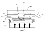
実装工程では、機械的手段(真空吸引による素子吸着)とレーザアブレーションの組み合わせにより発光ダイオード52(樹脂形成チップ)が第3の一時保持用部材64から剥離される。図27は、第3の一時保持用部材64上に配列している発光ダイオード52を吸着装置67でピックアップするところを示した図である。このときの吸着孔68は画像表示装置の画素ピッチにマトリクス状に開口していて、発光ダイオード52を多数個、一括で吸着できるようになっている。このときの開口径は、例えば直径約100μmで600μmピッチのマトリクス状に開口されて、一括で約300個を吸着できる。このときの吸着孔68の部材は例えば、Ni電鋳により作製したもの、もしくはSUSなどの金属板をエッチングで穴加工したものが使用され、吸着孔68の奥には吸着チャンバ69が形成されており、この吸着チャンバ69を負圧に制御することで発光ダイオード52の吸着が可能になる。発光ダイオード52はこの段階で樹脂層61で覆われており、その上面は略平坦化されている。このために吸着装置67による選択的な吸着を容易に進めることができる。
【0063】
なお、上記吸着装置67には、真空吸引による素子吸着の際に、発光ダイオード52(樹脂形成チップ)を一定の位置に安定して保持できるように、素子位置ずれ防止手段を形成しておくことが好ましい。図28は、素子位置ずれ防止手段70を設けた吸着装置67の一例を示すものである。本例では、素子位置ずれ防止手段70は、樹脂形成チップの周面に当接する位置決めピンとして形成されており、これが樹脂形成チップの周面(具体的にはレーザダイシングにより切断された樹脂層61の切断面)に当接することにより、吸着装置67と樹脂形成チップ(すなわち発光ダイオード52)とが互いに正確に位置合わせされる。上記レーザダイシングにより切断された樹脂層61の切断面は、完全な垂直面ではなく、5°〜10°程度のテーパ−を有する。したがって、上記位置決めピン(素子位置ずれ防止手段60)にも同様のテーパ−を持たせておけば、吸着装置67と発光ダイオード52間に若干の位置ずれがあったとしても、速やかに矯正される。
【0064】
上記発光ダイオード52の剥離に際しては、上記吸着装置67による素子吸着と、レーザアブレーションによる樹脂形成チップの剥離を組み合わせ、剥離が円滑に進むようにしている。レーザアブレーションは、第3の一時保持用部材64の裏面側からレーザを照射することにより行う。このレーザアブレーションによって、第3の一時保持用部材64と接着剤65の界面で剥離が生ずる。
【0065】
図29は発光ダイオード52を第二基板71に転写するところを示した図である。第二基板71は、配線層72を有する配線基板であり、発光ダイオード52を装着する際に第二基板71にあらかじめ接着剤層73が塗布されており、その発光ダイオード52下面の接着剤層73を硬化させ、発光ダイオード52を第二基板71に固着して配列させることができる。この装着時には、吸着装置67の吸着チャンバ69が圧力の高い状態となり、吸着装置67と発光ダイオード52との吸着による結合状態は解放される。接着剤層73はUV硬化型接着剤、熱硬化性接着剤、熱可塑性接着剤などによって構成することができる。第二基板71上で発光ダイオード52が配置される位置は、一時保持用部材64上での配列よりも離間したものとなる。接着剤層73の樹脂を硬化させるエネルギーは第二基板71の裏面から供給される。UV硬化型接着剤の場合はUV照射装置にて、熱硬化性接着剤の場合は赤外線加熱などによって発光ダイオード52の下面のみ硬化させ、熱可塑性接着剤場合は、赤外線やレーザの照射によって接着剤を溶融させ接着を行う。
【0066】
図30は、他の色の発光ダイオード74を第二基板71に配列させるプロセスを示す図である。図27あるいは図28で用いた吸着装置67をそのまま使用して、第二基板71にマウントする位置をその色の位置にずらすだけでマウントすると、画素としてのピッチは一定のまま複数色からなる画素を形成できる。ここで、発光ダイオード52と発光ダイオード74は必ずしも同じ形状でなくとも良い。図30では、赤色の発光ダイオード74が六角錐のGaN層を有しないプレーナ型構造とされ、他の発光ダイオード52とその形状が異なっているが、この段階では各発光ダイオード52、74は既に樹脂形成チップとして樹脂層61、接着剤65で覆われており、素子構造の違いにもかかわらず同一の取り扱いが実現される。
【0067】
次いで、図31に示すように、これら発光ダイオード52,74を含む樹脂形成チップを覆って絶縁層75を形成する。絶縁層75としては、透明エポキシ接着剤、UV硬化型接着剤、ポリイミドなどを用いることができる。上記絶縁層75を形成した後、配線形成工程を行なう。図32は配線形成工程を示す図である。絶縁層75に開口部76、77、78、79、80、81を形成し、発光ダイオード52、74のアノード、カソードの電極パッドと第二基板71の配線層72を接続する配線82、83、84を形成した図である。このときに形成する開口部すなわちビアホールは発光ダイオード52、74の電極パッドの面積を大きくしているので大きくすることができ、ビアホールの位置精度も各発光ダイオードに直接形成するビアホールに比べて粗い精度で形成できる。例えば、このときのビアホールは、約60μm角の電極パッドに対し、直径約20μmのものを形成できる。また、ビアホールの深さは配線基板と接続するもの、アノード電極と接続するもの、カソード電極と接続するものの3種類の深さがあるのでレーザのパルス数で制御し、最適な深さを開口する。
【0068】
その後、図33に示すように、保護層85を形成し、ブラックマスク86を形成して画像表示装置のパネルは完成する。このときの保護層85は図30の絶縁層75と同様であり、透明エポキシ接着剤などの材料が使用できる。この保護層85は加熱硬化し配線を完全に覆う。この後、パネル端部の配線からドライバーICを接続して駆動パネルを製作することになる。
【0069】
上述のような発光素子の配列方法においては、一時保持用部材59、64に発光ダイオード52を保持させた時点で既に、素子間の距離が大きくされ、その広がった間隔を利用して比較的サイズの電極パッド63、66などを設けることが可能となる。それら比較的サイズの大きな電極パッド63、66を利用した配線が行われるために、素子サイズに比較して最終的な装置のサイズが著しく大きな場合であっても容易に配線を形成できる。また、本例の発光素子の配列方法では、発光ダイオード52の周囲が硬化した樹脂層61で被覆され平坦化によって精度良く電極パッド63,66を形成できるとともに素子に比べて広い領域に電極パッド63,66を延在でき、次の第二転写工程での転写を吸着治具で進める場合には取り扱いが容易になる。
【0070】
【発明の効果】
以上の説明からも明らかなように、本発明の配線及びその形成方法によれば、従来のペーストを用いた配線形成に比べて工程数を削減することができ、またメッキ法に比べて簡単なプロセスとすることが可能である。また、形成される配線は、導電性に優れたものであり、微細配線も容易に実現することが可能である。同様に、本発明の接続孔及びその形成方法、配線形成体及びその形成方法によれば、簡単な手法で信頼性の高い接続孔、配線形成体の形成が可能である。
【0071】
また、本発明の表示素子の形成方法によれば、上記利点に加えて、発光素子を樹脂によりモジュール化した場合にも良好な電極形成が可能で、搬送や基体への実装も容易であるような構造を有し信頼性の高い表示素子を作製することができる。さらに、これら配線形成方法や発光素子の形成方法を応用することにより、生産性に優れ製造コストを抑えることが可能な画像表示装置の製造方法を提供することが可能である。
【図面の簡単な説明】
【図1】本発明を適用した配線形成方法の一例を示す概略断面図であり、(a)は溝形成工程、(b)は疎水化処理工程、(c)は微粒子型導電ペースト塗布工程、(d)は焼結工程をそれぞれ示す。
【図2】本発明を適用した配線形成方法の他の例を示す概略断面図であり、(a)は疎水化処理工程、(b)はフォトレジスト形成工程、(c)はエッチング工程、(d)はフォトレジスト除去工程、(e)は微粒子型導電ペースト塗布工程、(f)は焼結工程をそれぞれ示す。
【図3】本発明を適用した接続孔形成方法の一例を示す概略断面図であり、(a)は疎水化処理工程、(b)はフォトレジスト形成工程、(c)はエッチング工程、(d)はフォトレジスト除去工程、(e)は微粒子型導電ペースト塗布工程、(f)は焼結工程をそれぞれ示す。
【図4】本発明を適用した配線形成体の形成方法の一例を示す概略断面図であり、(a)は疎水化処理工程、(b)はフォトレジスト形成工程、(c)は溝エッチング工程、(d)は孔エッチング工程、(e)はフォトレジスト除去工程、(f)は微粒子型導電ペースト塗布工程、(g)は焼結工程をそれぞれ示す。
【図5】素子の配列方法を示す模式図である。
【図6】樹脂形成チップの概略斜視図である。
【図7】樹脂形成チップの概略平面図である。
【図8】発光素子の一例を示す図であって、(a)は断面図、(b)は平面図である。
【図9】第1の一時保持用部材の接合工程を示す概略断面図である。
【図10】UV接着剤硬化工程を示す概略断面図である。
【図11】レーザアブレーション工程を示す概略断面図である。
【図12】第一基板の分離工程を示す概略断面図である。
【図13】Ga除去工程を示す概略断面図である。
【図14】素子分離溝形成工程を示す概略断面図である。
【図15】第2の一時保持用部材の接合工程を示す概略断面図である。
【図16】選択的なレーザアブレーション及びUV露光工程を示す概略断面図である。
【図17】発光ダイオードの選択分離工程を示す概略断面図である。
【図18】樹脂による埋め込み工程を示す概略断面図である。
【図19】樹脂層厚削減工程を示す概略断面図である。
【図20】ビア形成工程を示す概略断面図である。
【図21】アノード側電極パッド形成工程を示す概略断面図である。
【図22】レーザアブレーション工程を示す概略断面図である。
【図23】第2の一時保持用部材の分離工程を示す概略断面図である。
【図24】コンタクト半導体層露出工程を示す概略断面図である。
【図25】カソード側電極パッド形成工程を示す概略断面図である。
【図26】レーザダイシング工程を示す概略断面図である。
【図27】吸着装置による選択的ピックアップ工程を示す概略断面図である。
【図28】素子位置ずれ防止手段を設けた吸着装置の一例を示す概略断面図である。
【図29】第二基板への転写工程を示す概略断面図である。
【図30】他の発光ダイオードの転写工程を示す概略断面図である。
【図31】絶縁層形成工程を示す概略断面図である。
【図32】配線形成工程を示す概略断面図である。
【図33】保護層及びブラックマスク形成工程を示す概略断面図である。
【符号の説明】
1 樹脂層、2 溝、3 疎水化層、4 微粒子型導電ペースト、5 配線パターン、7 孔、30 樹脂形成チップ、31 発光素子、32 樹脂、33,34 電極パッド、61 樹脂層、63,66 電極パッド[0001]
BACKGROUND OF THE INVENTION
The present invention relates to a wiring and a connection hole formed in a resin layer, and a method for forming the wiring, and further relates to a wiring forming body and a method for forming the wiring. The present invention also relates to a display element to which this is applied, a method for forming the same, an image display device, and a method for manufacturing the same.
[0002]
[Prior art]
For example, in the case where light emitting elements are arranged in a matrix and assembled into an image display device, conventionally, a liquid crystal display device (LCD: Liquid Crystal Display) or a plasma display panel (PDP: Plasma Display Panel) is used directly on a substrate. Elements are formed or a single LED package is arranged like a light emitting diode display (LED display). For example, in an image display device such as an LCD or PDP, since elements cannot be separated, each element is usually formed at an interval of the pixel pitch of the image display device from the beginning of the manufacturing process.
[0003]
On the other hand, in the case of an LED display, LED chips are taken out after dicing, and individually connected to external electrodes by wire bonding or bump connection by flip chip, and packaged. In this case, the pixels are arranged at a pixel pitch as an image display device before or after packaging, but this pixel pitch is independent of the element pitch at the time of element formation.
[0004]
Since LEDs (light emitting diodes), which are light emitting elements, are expensive, an image display device using LEDs can be manufactured at low cost by manufacturing a large number of LED chips from a single wafer. That is, if an LED chip having a size of about 300 μm square is changed to an LED chip of several tens μm square and connected to manufacture an image display apparatus, the price of the image display apparatus can be reduced.
[0005]
[Problems to be solved by the invention]
When an image display apparatus is manufactured by the transfer technique as described above, it is preferable that the light emitting element is formed into a chip component in order to realize efficient transfer and accurate transfer. Here, in order to make the light-emitting element into a chip component, the light-emitting element is embedded in a resin material, which is cut out and handled as a display element.
[0006]
By the way, when a light emitting element is embedded in a resin to form a chip component, it is necessary to form a wiring connected to the light emitting element on the resin and use this as an electrode for connection with the outside. Conventionally, in order to form a wiring made of metal on a resin, a method such as copper plating is generally used. However, in the case of the plating method, for example, if it is electrolytic plating, a layer that functions as an electrode is required in advance, and if it is electroless plating, it is difficult to control film formation. In addition, when a patterning process is performed after a film is formed on the entire surface by a plating method, there is a problem that the number of steps is large and complicated. In this regard, in the case of a printing method using a conductive paste, the number of steps can be reduced because the patterning is performed simultaneously with the film formation, but there remains a problem in terms of alignment accuracy with the lower layer pattern, for example.
[0007]
The present invention has been proposed in view of such conventional circumstances, and can reduce the number of steps, and can easily form a highly accurate wiring, a connecting hole, a wiring forming method, a connecting hole, It is an object of the present invention to provide a connection hole forming method, and further a wiring forming body and a forming method thereof.
[0008]
Another object of the present invention is to provide a method for forming a display element and a method for manufacturing an image display device to which this is applied. That is, even when the light emitting element is modularized with a resin, a good electrode can be formed, and a display element having a structure that can be easily transported and mounted on a substrate and can produce a highly reliable display element. An object of the present invention is to provide a forming method, and further to provide a manufacturing method of an image display device that is excellent in productivity and can suppress manufacturing costs.
[0009]
[Means for Solving the Problems]
In order to achieve the above-mentioned object, the wiring of the present invention is characterized in that a groove is formed in the resin layer according to the wiring pattern and the fine-particle conductive paste is sintered following the groove shape. To do. The wiring forming method of the present invention is a wiring forming method in which a metal wiring is formed on a resin layer, wherein a groove is formed in the resin layer in accordance with a wiring pattern, and the portion other than the groove is hydrophobic. Or after applying hydrophobization treatment to the resin layer and forming grooves in the resin layer according to the wiring pattern, applying a fine particle-type conductive paste and sintering it. A metal wiring following the groove shape is formed.
[0010]
When the fine particle type conductive paste is sintered after coating, the volume shrinks to about 1/5 to 1/10. At this time, if the resin surface is hydrophobized, the fine particle type conductive paste is hydrophobized. It is repelled on the resin surface and is selectively formed only in the groove. Thereby, a wiring pattern is formed in a so-called self-alignment. The fine particle type conductive paste is formed by dispersing very fine metal nanoparticles, can form a fine wiring pattern, and has high electrical reliability.
[0011]
Furthermore, the connection hole of the present invention is characterized in that a connection hole is formed in the resin layer, and the fine particle type conductive paste is filled in the hole and sintered. Further, the connection hole forming method of the present invention is a connection hole forming method for forming a connection hole filled with a conductive material on a resin layer, wherein a connection hole is formed in the resin layer, and a portion other than the hole is formed. After applying a hydrophobic treatment to the resin layer, or after applying a hydrophobic treatment to the resin layer to form a connection hole in the resin layer, a fine particle type conductive paste is applied to the hole. And is sintered.
[0012]
Since the fine particle type conductive paste can be reduced in viscosity, it can be easily filled into fine holes. As described above, after forming holes in the resin layer and applying a hydrophobic treatment to the resin layer other than the holes, the fine particle type conductive paste is self-aligned in the holes. Filled and so-called through holes (connection holes) are easily formed.
[0013]
Furthermore, in the wiring formed body of the present invention, a groove is formed in the resin layer according to the wiring pattern and a connection hole is formed, and the fine particle type conductive paste is sintered following the groove shape, The hole is filled with a fine particle type conductive paste and sintered. Further, the method for forming a wiring formed body according to the present invention includes forming a groove in the resin layer according to the wiring pattern and forming a connection hole, and hydrophobizing the resin layer in a portion other than the groove and the hole. Or after hydrophobizing the resin layer, forming grooves in the resin layer according to the wiring pattern and forming connection holes, and then applying a fine particle type conductive paste. By sintering, the metal wiring following the groove shape and the connection hole in which the hole is filled with a conductive material are formed. In this wiring forming body and its forming method, the wiring forming and the connection hole forming are simultaneously performed in a self-aligning manner.
[0014]
Furthermore, in the display element of the present invention, a light emitting element is embedded in a resin to form a chip component, and a groove is formed on the resin surface. A fine particle type conductive paste is sintered along the groove shape to form an electrode. It is characterized by being. The display element forming method of the present invention is a display element forming method in which a light emitting element is embedded in a resin to form a chip component, and then an electrode is formed on the resin surface. After applying the hydrophobic treatment to the resin other than the groove or forming the groove according to the wiring pattern on the resin surface by applying the hydrophobic treatment to the resin, the fine particles An electrode that follows the groove shape is formed by applying a mold-type conductive paste and sintering the paste. In such a display element or a method for forming a display element, a fine electrode can be easily and reliably formed, and its electrical reliability is high.
[0015]
Furthermore, the image display device of the present invention is an image display device in which light-emitting elements are embedded in a resin and display elements formed into chip parts are arranged in a matrix, and the display element has grooves formed on the resin surface. According to the groove shape, the fine particle type conductive paste is sintered to form an electrode. In addition, in the method for manufacturing an image display device of the present invention, the light emitting element is transferred so that the light emitting element is separated from the arrayed state on the first substrate, and the light emitting element is placed on the temporary holding member. Forming a first transfer step of holding, a second transfer step of transferring the light emitting elements held on the temporary holding member further apart and transferring them onto the second substrate, and wiring connected to the light emitting elements. In a manufacturing method of an image display device having a wiring formation step and arranging a display element in which a light emitting element is embedded in a resin and formed into a chip part in a matrix shape, the light emitting element is embedded in a resin to form a chip part, A groove is formed on the resin surface in accordance with the wiring pattern, and the resin other than the groove is subjected to a hydrophobic treatment, or the resin is subjected to a hydrophobic treatment to form a wiring pattern on the resin surface. After forming the grooves according, particulate-type conductive paste is applied, it is characterized in that to form an electrode following the above groove shape by sintering it.
[0016]
In the display element and the image display apparatus of the present invention, the light emitting element is embedded in a resin and modularized to form a display element. In this way, if the light-emitting elements that are finely formed are embedded in a resin and reshaped to a size that is easy to handle and modularized, the manufacturing cost can be suppressed to the limit, and at the same time, handleability can be ensured. Is also easy. Further, by driving and forming the drive electrodes of the light emitting elements on the surface of the modularized display element, the power lines and signal lines formed on the base can be easily connected to these drive electrodes. It is also very easy to implement in
[0017]
DETAILED DESCRIPTION OF THE INVENTION
Hereinafter, a wiring and a method for forming the same, a connection hole and a method for forming the same, a wiring forming body and a method for forming the same, a display element and a method for forming the same, an image display device and a method for manufacturing the same to which the present invention is applied will be described in detail with reference to the drawings. Explained.
[0018]
First, in the wiring and the wiring forming method of the present invention, the basic idea is to form a groove in the resin layer and form a wiring pattern of the fine-particle conductive paste in a self-aligning manner here. FIG. 1 shows an example of a wiring forming method to which the present invention is applied according to the order of steps. In this example, as shown in FIG. 1A, a
[0019]
Next, as shown in FIG. 1B, the surface of the resin layer 1 other than the
[0020]
Thus, after hydrophobizing a part other than the groove |
[0021]
The fine particle type conductive paste is obtained by uniformly dispersing fine conductive particles having a particle size of 100 nm or less (for example, about 7 nm) formed by, for example, a gas evaporation method, and does not aggregate even at a high metal content at room temperature. It can be handled like a liquid and can be applied to a microstructured surface. Specific examples include nano paste made by Harima Chemicals. This nanopaste is a dispersion of independent dispersed silver nanoparticles uniformly in a thermosetting resin. When heated to a certain temperature, the supplementary substance is activated to chemically remove the dispersant and the surrounding resin By curing and shrinking, the nanoparticles are brought into contact with each other, and fusion and fusion are accelerated to form wiring. The wiring obtained by sintering this has sufficient conductivity because the ultrafine particles are fused and fused.
[0022]
After the fine particle type conductive paste 4 is applied, it is heated and sintered. The heating temperature is about 200 ° C. Then, the particulate conductive paste 4 shrinks to a volume of about 1/5 to 1/10. Here, if the coating amount of the fine particle type conductive paste 4 is set so that the volume after shrinkage is substantially the same as the volume of the
[0023]
In the above example, the
[0024]
Hereinafter, a process example in which the
[0025]
Next, as shown in FIG. 2D, the
[0026]
The above method can also be applied to the formation of connection holes (so-called through holes). Hereinafter, an example of a method for forming a connection hole to which the present invention is applied will be described with reference to FIG. In this connection hole formation, either the formation of the hole in the resin layer or the hydrophobic treatment may be performed first, but here the hydrophobic treatment is performed first and the hole in the resin layer is formed. A case where the formation is performed later will be described as an example.
[0027]
In order to form the connection hole, as shown in FIG. 3A, a hydrophobic treatment is performed on the resin layer 1 to form a
[0028]
Next, as shown in FIG. 3D, the
[0029]
As described above, the connection hole can be easily formed by applying the present invention, but it is also possible to proceed one step further and simultaneously perform the wiring formation and the connection hole formation. FIG. 4 shows an example of a method for forming a wiring forming body in which wiring formation and connection hole formation are performed simultaneously. In this example as well, either the formation of grooves or holes in the resin layer or the hydrophobic treatment may be performed first, but here the hydrophobic treatment is performed first and the grooves and holes in the resin layer are performed. The case where the formation is performed later will be described as an example.
[0030]
In order to form a wiring formation body, as shown in FIG. 4A, a hydrophobic treatment is performed on the resin layer 1 to form a
[0031]
Next, as shown in FIG. 4E, the
[0032]
The wiring forming method can be applied to, for example, a method for forming a display element in which a light emitting element is embedded in a resin to form a chip component, and then an electrode is formed on the resin surface. Hereinafter, a method for forming the display element and a method for manufacturing the image display device will be described.
[0033]
For example, when an image display device is manufactured using light emitting diodes, the light emitting diodes need to be arranged separately. There are various arrangement methods, and here, a two-step enlarged transfer method will be described as an example. In the two-stage enlarged transfer method, first, an element formed on a first substrate with a high degree of integration is transferred to a temporary holding member so that the element is separated from the state in which the elements are arranged on the first substrate. Subsequently, two-stage enlarged transfer is performed in which the element held by the temporary holding member is further separated and transferred onto the second substrate. In this example, the transfer is performed in two stages. However, the transfer can be performed in three or more stages depending on the degree of enlargement in which the elements are spaced apart.
[0034]
FIG. 5 is a diagram showing the basic steps of the two-stage enlarged transfer method. First,
[0035]
Next, as shown in FIG. 5B, each
[0036]
After such a first transfer step, as shown in FIG. 5C, the
[0037]
Next, as shown in FIG. 5D, a second transfer process is performed. In this second transfer step, the
[0038]
Wiring is applied to each
[0039]
In the two-stage enlarged transfer method shown in FIG. 5, the electrode pad can be formed using the spaced space after the first transfer, and the wiring is applied after the second transfer. Wiring is performed while using the formed electrode pads or the like to suppress connection failures as much as possible. Therefore, the yield of the image display device can be improved. Further, in the two-stage enlargement transfer method of this example, the process of separating the distance between the elements is two processes, and the number of times of transfer is actually increased by performing such multiple processes of separating the distance between the elements. Will be reduced. That is, for example, the enlargement ratio of the pitches separated from the first substrates 20 and 20a by the
[0040]
In the two-stage enlarged transfer method shown in FIG. 5, the
[0041]
In the second transfer step, the light emitting element is handled as a resin-formed chip and is transferred onto the second substrate from the temporary holding member. The resin-formed chip will be described with reference to FIGS. 6 and 7. . The resin-formed chip 30 is obtained by fixing the periphery of the light-emitting elements 31 that are spaced apart with a resin 32. The resin-formed chip 30 is configured such that the light-emitting elements 31 are placed on the second substrate from the temporary holding member. It can be used when transferring. The resin-formed chip 30 has a substantially flat plate shape and a main surface of the chip. The shape of the resin-forming chip 30 is a shape formed by solidifying the resin 32. Specifically, an uncured resin is applied to the entire surface so as to include the respective light emitting elements 31, and after this is cured, the edge is formed. It is a shape obtained by cutting a part by dicing or the like.
[0042]
Electrode pads 33 and 34 are formed on the front side and the back side of the substantially flat resin 32, respectively. The electrode pads 33 and 34 are formed by forming a conductive layer such as a metal layer or a polycrystalline silicon layer as a material of the electrode pads 33 and 34 on the entire surface, and patterning it into a required electrode shape by a photolithography technique. Is done. These electrode pads 33 and 34 are formed so as to be connected to the p-electrode and the n-electrode, respectively, of the light emitting element 31, and a via hole or the like is formed in the resin 32 when necessary. The wiring forming method can be applied to the formation of the electrode pads 33 and 34. The electrode pads 33 and 34 are formed with grooves in the resin 32 in accordance with the shape of the electrode pads, and a fine particle type conductive paste is used. It is formed in a self-aligned manner by applying and sintering.
[0043]
Here, the electrode pads 33 and 34 are respectively formed on the front surface side and the back surface side of the resin-formed chip 30, but both electrode pads can be formed on one surface. For example, in the case of a thin film transistor, Since there are three electrodes, gate and drain, three or more electrode pads may be formed. The reason why the positions of the electrode pads 33 and 34 are shifted from each other on the flat plate is to prevent the electrode pads 33 and 34 from overlapping even when contacts are made from the upper side when the final wiring is formed. The shape of the electrode pads 33 and 34 is not limited to a square, and may be other shapes.
[0044]
By constructing such a resin-formed chip 30, the periphery of the light emitting element 31 is covered with the resin 32, and the electrode pads 33 and 34 can be formed with high accuracy by flattening. , 34 can be extended, and handling is facilitated when the transfer in the next second transfer step is advanced by a suction jig. As will be described later, since the final wiring is performed after the second transfer step, the wiring defect is prevented by performing the wiring using the electrode pads 33 and 34 having a relatively large size.
[0045]
Next, FIG. 8 shows a structure of a light emitting element as an example of an element used in the two-stage enlarged transfer method of this example. FIG. 8A is an element cross-sectional view, and FIG. 8B is a plan view. This light-emitting element is a GaN-based light-emitting diode, for example, an element that is crystal-grown on a sapphire substrate. In such a GaN-based light emitting diode, laser ablation occurs due to laser irradiation that passes through the substrate, and film peeling occurs at the interface between the sapphire substrate and the GaN-based growth layer due to the phenomenon of nitrogen vaporization of GaN, It has a feature that element isolation can be made easy.
[0046]
First, with respect to the structure, a hexagonal pyramid-shaped
[0047]
In such a light emitting diode, a p-
[0048]
A GaN-based light emitting diode with such a structure is an element capable of emitting blue light, and can be peeled off from a sapphire substrate relatively easily by laser ablation, and is selected by selectively irradiating a laser beam. Exfoliation is realized. The GaN-based light emitting diode may have a structure in which an active layer is formed on a flat plate or in a strip shape, or may have a pyramid structure in which a C surface is formed at the upper end. Further, other nitride-based light emitting elements, compound semiconductor elements, and the like may be used.
[0049]
Next, a specific method for manufacturing an image display device to which the light emitting element arrangement method shown in FIG. 5 is applied will be described. As the light emitting element, the GaN-based light emitting diode shown in FIG. 8 is used. First, as shown in FIG. 9, a plurality of
[0050]
Next, the
[0051]
At the time of transfer, as shown in FIG. 9, an adhesive (for example, an ultraviolet curable adhesive) 55 sufficient to cover the
[0052]
At this time, since the first temporary holding
[0053]
After the adhesive 55 is cured, as shown in FIG. 11, a laser is irradiated from the back surface of the
[0054]
FIG. 12 shows a state where the
[0055]
In order to selectively separate the
[0056]
Next, as shown in FIG. 16, only the position corresponding to the light-emitting
[0057]
After the selective separation, as shown in FIG. 18, a resin is applied to cover the transferred
[0058]
Next, an anode
[0059]
After the
[0060]
In the formation of the cathode side electrode, after passing through the above transfer step, the O shown in FIG. 2 The
[0061]
Next, the
[0062]
In the mounting process, the light-emitting diode 52 (resin-formed chip) is peeled from the third temporary holding
[0063]
The
[0064]
When the
[0065]
FIG. 29 is a view showing a state where the
[0066]
FIG. 30 is a diagram illustrating a process of arranging the
[0067]
Next, as shown in FIG. 31, an insulating
[0068]
Thereafter, as shown in FIG. 33, a
[0069]
In the light emitting element arrangement method as described above, the distance between the elements is already increased at the time when the
[0070]
【Effect of the invention】
As is clear from the above description, according to the wiring of the present invention and the method for forming the wiring, the number of processes can be reduced as compared with the conventional wiring formation using the paste, and simpler than the plating method. It can be a process. In addition, the formed wiring has excellent conductivity, and fine wiring can be easily realized. Similarly, according to the connection hole and the formation method thereof, the wiring formation body and the formation method of the present invention, a highly reliable connection hole and wiring formation body can be formed by a simple method.
[0071]
Further, according to the method for forming a display element of the present invention, in addition to the above advantages, it is possible to form a good electrode even when the light emitting element is modularized with a resin, and it is easy to carry and mount on a substrate. A highly reliable display element having a simple structure can be manufactured. Furthermore, by applying these wiring forming method and light emitting element forming method, it is possible to provide a manufacturing method of an image display device that is excellent in productivity and can suppress manufacturing costs.
[Brief description of the drawings]
FIG. 1 is a schematic cross-sectional view showing an example of a wiring forming method to which the present invention is applied, in which (a) is a groove forming step, (b) is a hydrophobizing treatment step, (c) is a fine particle type conductive paste applying step, (D) shows a sintering process, respectively.
FIGS. 2A and 2B are schematic cross-sectional views showing another example of a wiring forming method to which the present invention is applied, in which FIG. 2A is a hydrophobizing treatment step, FIG. 2B is a photoresist forming step, FIG. 2C is an etching step, d) shows a photoresist removing step, (e) shows a fine particle type conductive paste coating step, and (f) shows a sintering step.
3A and 3B are schematic cross-sectional views showing an example of a connection hole forming method to which the present invention is applied, in which FIG. 3A is a hydrophobizing treatment step, FIG. 3B is a photoresist forming step, FIG. 3C is an etching step, and FIG. ) Shows a photoresist removal step, (e) shows a fine-particle type conductive paste coating step, and (f) shows a sintering step.
4A and 4B are schematic cross-sectional views showing an example of a method for forming a wiring formed body to which the present invention is applied, in which FIG. 4A is a hydrophobization treatment step, FIG. 4B is a photoresist formation step, and FIG. 4C is a groove etching step. , (D) shows a hole etching step, (e) shows a photoresist removal step, (f) shows a fine particle type conductive paste coating step, and (g) shows a sintering step.
FIG. 5 is a schematic diagram showing a method of arranging elements.
FIG. 6 is a schematic perspective view of a resin-formed chip.
FIG. 7 is a schematic plan view of a resin-formed chip.
8A and 8B are diagrams illustrating an example of a light-emitting element, in which FIG. 8A is a cross-sectional view, and FIG. 8B is a plan view.
FIG. 9 is a schematic cross-sectional view showing a first temporary holding member joining step.
FIG. 10 is a schematic cross-sectional view showing a UV adhesive curing step.
FIG. 11 is a schematic cross-sectional view showing a laser ablation process.
FIG. 12 is a schematic cross-sectional view showing a first substrate separation step.
FIG. 13 is a schematic cross-sectional view showing a Ga removal step.
FIG. 14 is a schematic cross-sectional view showing an element isolation groove forming step.
FIG. 15 is a schematic cross-sectional view showing a joining process of a second temporary holding member.
FIG. 16 is a schematic cross-sectional view showing a selective laser ablation and UV exposure process.
FIG. 17 is a schematic cross-sectional view showing a selective separation process of light emitting diodes.
FIG. 18 is a schematic sectional view showing a resin embedding step.
FIG. 19 is a schematic cross-sectional view showing a resin layer thickness reduction step.
FIG. 20 is a schematic cross-sectional view showing a via formation step.
FIG. 21 is a schematic cross-sectional view showing an anode-side electrode pad forming step.
FIG. 22 is a schematic sectional view showing a laser ablation process.
FIG. 23 is a schematic cross-sectional view showing a separation process of a second temporary holding member.
FIG. 24 is a schematic cross-sectional view showing a contact semiconductor layer exposing step.
FIG. 25 is a schematic cross-sectional view showing a cathode-side electrode pad forming step.
FIG. 26 is a schematic sectional view showing a laser dicing process.
FIG. 27 is a schematic cross-sectional view showing a selective pickup process by the adsorption device.
FIG. 28 is a schematic cross-sectional view showing an example of a suction device provided with element position deviation prevention means.
FIG. 29 is a schematic cross-sectional view showing a transfer process to a second substrate.
FIG. 30 is a schematic cross-sectional view showing another light-emitting diode transfer step.
FIG. 31 is a schematic cross-sectional view showing an insulating layer forming step.
FIG. 32 is a schematic cross-sectional view showing a wiring formation step.
FIG. 33 is a schematic cross-sectional view showing a protective layer and black mask forming step.
[Explanation of symbols]
DESCRIPTION OF SYMBOLS 1 Resin layer, 2 groove | channel, 3 Hydrophobization layer, 4 Fine particle type electrically conductive paste, 5 Wiring pattern, 7 hole, 30 Resin formation chip, 31 Light emitting element, 32 Resin, 33, 34 Electrode pad, 61 Resin layer, 63, 66 Electrode pad
Claims (2)
Priority Applications (1)
| Application Number | Priority Date | Filing Date | Title |
|---|---|---|---|
| JP2001265595A JP4982932B2 (en) | 2001-09-03 | 2001-09-03 | Manufacturing method of image display device |
Applications Claiming Priority (1)
| Application Number | Priority Date | Filing Date | Title |
|---|---|---|---|
| JP2001265595A JP4982932B2 (en) | 2001-09-03 | 2001-09-03 | Manufacturing method of image display device |
Publications (2)
| Publication Number | Publication Date |
|---|---|
| JP2003078171A JP2003078171A (en) | 2003-03-14 |
| JP4982932B2 true JP4982932B2 (en) | 2012-07-25 |
Family
ID=19092037
Family Applications (1)
| Application Number | Title | Priority Date | Filing Date |
|---|---|---|---|
| JP2001265595A Expired - Fee Related JP4982932B2 (en) | 2001-09-03 | 2001-09-03 | Manufacturing method of image display device |
Country Status (1)
| Country | Link |
|---|---|
| JP (1) | JP4982932B2 (en) |
Cited By (1)
| Publication number | Priority date | Publication date | Assignee | Title |
|---|---|---|---|---|
| KR101435255B1 (en) * | 2012-06-22 | 2014-08-29 | 서울과학기술대학교 산학협력단 | Circuit Board Prepared by Nanoparticle Alignment, Guided through Interfacial Interaction and Microfabricated Structure on Substrate, the pattern printing method thereof and the manufacturing method for mold therefor |
Families Citing this family (17)
| Publication number | Priority date | Publication date | Assignee | Title |
|---|---|---|---|---|
| AU2001268411A1 (en) | 2000-06-14 | 2002-01-02 | Core Express, Inc. | Route selection within a network with peering connections |
| JP4484578B2 (en) * | 2004-05-11 | 2010-06-16 | 株式会社リコー | Pattern shape body and method for manufacturing the same |
| JP4146826B2 (en) | 2004-09-14 | 2008-09-10 | カシオマイクロニクス株式会社 | Wiring substrate and semiconductor device |
| KR100999919B1 (en) * | 2008-09-08 | 2010-12-13 | 삼성전기주식회사 | Printed Circuit Board Manufacturing Method |
| JP5376136B2 (en) * | 2009-04-02 | 2013-12-25 | ソニー株式会社 | Pattern formation method |
| JP2011029256A (en) * | 2009-07-22 | 2011-02-10 | Tokyo Electron Ltd | Film forming method |
| JP5729932B2 (en) * | 2010-07-22 | 2015-06-03 | キヤノン株式会社 | Method of filling metal into substrate through hole |
| JP2012083962A (en) * | 2010-10-12 | 2012-04-26 | Innovation & Infinity Global Corp | Method of manufacturing metal circuit of touch panel, and touch panel |
| KR101820326B1 (en) * | 2010-11-30 | 2018-01-22 | 삼성디스플레이 주식회사 | Display substrate and method of manufacturing the same |
| JP6095315B2 (en) * | 2012-10-02 | 2017-03-15 | キヤノン株式会社 | Method for manufacturing liquid discharge head |
| CN102903423B (en) * | 2012-10-25 | 2015-05-13 | 南昌欧菲光科技有限公司 | Conduction structure in transparent conduction film, transparent conduction film and manufacture method thereof |
| KR101976558B1 (en) * | 2015-03-25 | 2019-05-09 | 주식회사 엘지화학 | Buried wiring and method of thereof |
| JP7402706B2 (en) * | 2020-02-10 | 2023-12-21 | アオイ電子株式会社 | Method for manufacturing a light emitting device, and light emitting device |
| JP7469092B2 (en) | 2020-03-23 | 2024-04-16 | 株式会社Screenホールディングス | Cell Retention Container |
| CN115483242A (en) * | 2021-05-31 | 2022-12-16 | 重庆康佳光电技术研究院有限公司 | Display backboard, display assembly, manufacturing method and detection and repair method |
| JP7743733B2 (en) * | 2021-08-31 | 2025-09-25 | 富士電機株式会社 | Semiconductor device manufacturing method |
| CN113921464A (en) * | 2021-09-17 | 2022-01-11 | 上海华虹宏力半导体制造有限公司 | Method for manufacturing back metal layer |
Family Cites Families (9)
| Publication number | Priority date | Publication date | Assignee | Title |
|---|---|---|---|---|
| JPS58130582A (en) * | 1982-01-29 | 1983-08-04 | Toshiba Corp | Display device |
| JPH02262393A (en) * | 1989-04-03 | 1990-10-25 | Toshiba Corp | Formation of circuit pattern |
| JPH0317656U (en) * | 1989-06-30 | 1991-02-21 | ||
| JPH0340430A (en) * | 1990-07-06 | 1991-02-21 | Hitachi Ltd | Semiconductor device |
| JPH08203891A (en) * | 1995-01-27 | 1996-08-09 | Sharp Corp | Method for manufacturing semiconductor device |
| JPH10135088A (en) * | 1996-11-05 | 1998-05-22 | Matsushita Electric Ind Co Ltd | Electronic component manufacturing method |
| JP4011695B2 (en) * | 1996-12-02 | 2007-11-21 | 株式会社東芝 | Chip for multi-chip semiconductor device and method for forming the same |
| JP3510479B2 (en) * | 1998-04-27 | 2004-03-29 | シャープ株式会社 | Manufacturing method of optical input / output element array device |
| JP3356122B2 (en) * | 1999-07-08 | 2002-12-09 | 日本電気株式会社 | System semiconductor device and method of manufacturing system semiconductor device |
-
2001
- 2001-09-03 JP JP2001265595A patent/JP4982932B2/en not_active Expired - Fee Related
Cited By (1)
| Publication number | Priority date | Publication date | Assignee | Title |
|---|---|---|---|---|
| KR101435255B1 (en) * | 2012-06-22 | 2014-08-29 | 서울과학기술대학교 산학협력단 | Circuit Board Prepared by Nanoparticle Alignment, Guided through Interfacial Interaction and Microfabricated Structure on Substrate, the pattern printing method thereof and the manufacturing method for mold therefor |
Also Published As
| Publication number | Publication date |
|---|---|
| JP2003078171A (en) | 2003-03-14 |
Similar Documents
| Publication | Publication Date | Title |
|---|---|---|
| US6972204B2 (en) | Method of transferring devices, method of arranging devices using the same, and method of manufacturing an image display system | |
| JP4055405B2 (en) | Electronic component and manufacturing method thereof | |
| JP3747807B2 (en) | Device mounting substrate and defective device repair method | |
| JP3994681B2 (en) | Element arrangement method and image display device manufacturing method | |
| JP3608615B2 (en) | Device transfer method, device array method using the same, and image display device manufacturing method | |
| US7008827B2 (en) | Alloy method using laser irradiation | |
| JP3890921B2 (en) | Element arrangement method and image display device manufacturing method | |
| JP4120223B2 (en) | Electronic component manufacturing method and image display apparatus using the same | |
| JP4450067B2 (en) | Electronic component, method for manufacturing the same, and image display apparatus using the same | |
| JP4078825B2 (en) | Circuit board manufacturing method and display device manufacturing method | |
| WO2002086964A1 (en) | Wiring method and element arranging method using the same, and method of producing image display devices | |
| JP2003078171A (en) | Wiring and forming method thereof, connection hole and forming method thereof, wiring forming body and forming method thereof, display element and forming method thereof, image display device and manufacturing method thereof | |
| JP2003098977A (en) | Element transfer method, element arrangement method, and image display device manufacturing method | |
| US20200075564A1 (en) | Light-emitting diode package structure and manufacturing method thereof | |
| JP2003347524A (en) | Element transfer method, element arrangement method, and image display device manufacturing method | |
| JP2002343944A (en) | Electronic component transfer method, element arrangement method, and image display device manufacturing method | |
| JP2002314053A (en) | Method for transferring chip components, method for arranging elements using the same, and method for manufacturing image display device | |
| JP4882273B2 (en) | Device mounting substrate, defective device repair method, and image display device | |
| JP2003162231A (en) | Element manufacturing method, element arranging method, and image display apparatus manufacturing method | |
| JP2002314123A (en) | Element transfer method, element arrangement method using the same, and image display device manufacturing method | |
| JP4848606B2 (en) | Element positioning method, element extraction method, element transfer method, element arrangement method, and image display device manufacturing method | |
| JP2002158237A (en) | Device transfer method and device mounting method | |
| JP4967251B2 (en) | Manufacturing method of image display device | |
| JP4839533B2 (en) | Image display device and manufacturing method thereof | |
| JP5176260B2 (en) | Manufacturing method of image display device |
Legal Events
| Date | Code | Title | Description |
|---|---|---|---|
| RD04 | Notification of resignation of power of attorney |
Free format text: JAPANESE INTERMEDIATE CODE: A7424 Effective date: 20050516 |
|
| RD03 | Notification of appointment of power of attorney |
Free format text: JAPANESE INTERMEDIATE CODE: A7423 Effective date: 20050527 |
|
| A621 | Written request for application examination |
Free format text: JAPANESE INTERMEDIATE CODE: A621 Effective date: 20080708 |
|
| A977 | Report on retrieval |
Free format text: JAPANESE INTERMEDIATE CODE: A971007 Effective date: 20110713 |
|
| A131 | Notification of reasons for refusal |
Free format text: JAPANESE INTERMEDIATE CODE: A131 Effective date: 20111220 |
|
| A521 | Request for written amendment filed |
Free format text: JAPANESE INTERMEDIATE CODE: A523 Effective date: 20120214 |
|
| TRDD | Decision of grant or rejection written | ||
| A01 | Written decision to grant a patent or to grant a registration (utility model) |
Free format text: JAPANESE INTERMEDIATE CODE: A01 Effective date: 20120327 |
|
| A01 | Written decision to grant a patent or to grant a registration (utility model) |
Free format text: JAPANESE INTERMEDIATE CODE: A01 |
|
| A61 | First payment of annual fees (during grant procedure) |
Free format text: JAPANESE INTERMEDIATE CODE: A61 Effective date: 20120409 |
|
| FPAY | Renewal fee payment (event date is renewal date of database) |
Free format text: PAYMENT UNTIL: 20150511 Year of fee payment: 3 |
|
| LAPS | Cancellation because of no payment of annual fees |