JP4982948B2 - 半導体装置の製造方法 - Google Patents
半導体装置の製造方法 Download PDFInfo
- Publication number
- JP4982948B2 JP4982948B2 JP2005017486A JP2005017486A JP4982948B2 JP 4982948 B2 JP4982948 B2 JP 4982948B2 JP 2005017486 A JP2005017486 A JP 2005017486A JP 2005017486 A JP2005017486 A JP 2005017486A JP 4982948 B2 JP4982948 B2 JP 4982948B2
- Authority
- JP
- Japan
- Prior art keywords
- conductivity type
- main surface
- groove
- region
- separation layer
- Prior art date
- Legal status (The legal status is an assumption and is not a legal conclusion. Google has not performed a legal analysis and makes no representation as to the accuracy of the status listed.)
- Expired - Fee Related
Links
Images









Classifications
-
- H—ELECTRICITY
- H10—SEMICONDUCTOR DEVICES; ELECTRIC SOLID-STATE DEVICES NOT OTHERWISE PROVIDED FOR
- H10D—INORGANIC ELECTRIC SEMICONDUCTOR DEVICES
- H10D12/00—Bipolar devices controlled by the field effect, e.g. insulated-gate bipolar transistors [IGBT]
- H10D12/411—Insulated-gate bipolar transistors [IGBT]
-
- H—ELECTRICITY
- H10—SEMICONDUCTOR DEVICES; ELECTRIC SOLID-STATE DEVICES NOT OTHERWISE PROVIDED FOR
- H10D—INORGANIC ELECTRIC SEMICONDUCTOR DEVICES
- H10D12/00—Bipolar devices controlled by the field effect, e.g. insulated-gate bipolar transistors [IGBT]
- H10D12/01—Manufacture or treatment
- H10D12/031—Manufacture or treatment of IGBTs
- H10D12/032—Manufacture or treatment of IGBTs of vertical IGBTs
-
- H—ELECTRICITY
- H10—SEMICONDUCTOR DEVICES; ELECTRIC SOLID-STATE DEVICES NOT OTHERWISE PROVIDED FOR
- H10D—INORGANIC ELECTRIC SEMICONDUCTOR DEVICES
- H10D12/00—Bipolar devices controlled by the field effect, e.g. insulated-gate bipolar transistors [IGBT]
- H10D12/411—Insulated-gate bipolar transistors [IGBT]
- H10D12/441—Vertical IGBTs
-
- H—ELECTRICITY
- H10—SEMICONDUCTOR DEVICES; ELECTRIC SOLID-STATE DEVICES NOT OTHERWISE PROVIDED FOR
- H10D—INORGANIC ELECTRIC SEMICONDUCTOR DEVICES
- H10D62/00—Semiconductor bodies, or regions thereof, of devices having potential barriers
- H10D62/10—Shapes, relative sizes or dispositions of the regions of the semiconductor bodies; Shapes of the semiconductor bodies
- H10D62/102—Constructional design considerations for preventing surface leakage or controlling electric field concentration
- H10D62/103—Constructional design considerations for preventing surface leakage or controlling electric field concentration for increasing or controlling the breakdown voltage of reverse-biased devices
- H10D62/104—Constructional design considerations for preventing surface leakage or controlling electric field concentration for increasing or controlling the breakdown voltage of reverse-biased devices having particular shapes of the bodies at or near reverse-biased junctions, e.g. having bevels or moats
-
- H—ELECTRICITY
- H10—SEMICONDUCTOR DEVICES; ELECTRIC SOLID-STATE DEVICES NOT OTHERWISE PROVIDED FOR
- H10D—INORGANIC ELECTRIC SEMICONDUCTOR DEVICES
- H10D62/00—Semiconductor bodies, or regions thereof, of devices having potential barriers
- H10D62/10—Shapes, relative sizes or dispositions of the regions of the semiconductor bodies; Shapes of the semiconductor bodies
- H10D62/113—Isolations within a component, i.e. internal isolations
- H10D62/114—PN junction isolations
-
- H—ELECTRICITY
- H10—SEMICONDUCTOR DEVICES; ELECTRIC SOLID-STATE DEVICES NOT OTHERWISE PROVIDED FOR
- H10D—INORGANIC ELECTRIC SEMICONDUCTOR DEVICES
- H10D62/00—Semiconductor bodies, or regions thereof, of devices having potential barriers
- H10D62/10—Shapes, relative sizes or dispositions of the regions of the semiconductor bodies; Shapes of the semiconductor bodies
- H10D62/113—Isolations within a component, i.e. internal isolations
- H10D62/115—Dielectric isolations, e.g. air gaps
-
- H—ELECTRICITY
- H10—SEMICONDUCTOR DEVICES; ELECTRIC SOLID-STATE DEVICES NOT OTHERWISE PROVIDED FOR
- H10D—INORGANIC ELECTRIC SEMICONDUCTOR DEVICES
- H10D62/00—Semiconductor bodies, or regions thereof, of devices having potential barriers
- H10D62/10—Shapes, relative sizes or dispositions of the regions of the semiconductor bodies; Shapes of the semiconductor bodies
- H10D62/117—Shapes of semiconductor bodies
-
- H—ELECTRICITY
- H10—SEMICONDUCTOR DEVICES; ELECTRIC SOLID-STATE DEVICES NOT OTHERWISE PROVIDED FOR
- H10D—INORGANIC ELECTRIC SEMICONDUCTOR DEVICES
- H10D62/00—Semiconductor bodies, or regions thereof, of devices having potential barriers
- H10D62/10—Shapes, relative sizes or dispositions of the regions of the semiconductor bodies; Shapes of the semiconductor bodies
- H10D62/13—Semiconductor regions connected to electrodes carrying current to be rectified, amplified or switched, e.g. source or drain regions
- H10D62/141—Anode or cathode regions of thyristors; Collector or emitter regions of gated bipolar-mode devices, e.g. of IGBTs
- H10D62/142—Anode regions of thyristors or collector regions of gated bipolar-mode devices
-
- H—ELECTRICITY
- H10—SEMICONDUCTOR DEVICES; ELECTRIC SOLID-STATE DEVICES NOT OTHERWISE PROVIDED FOR
- H10D—INORGANIC ELECTRIC SEMICONDUCTOR DEVICES
- H10D62/00—Semiconductor bodies, or regions thereof, of devices having potential barriers
- H10D62/40—Crystalline structures
- H10D62/405—Orientations of crystalline planes
-
- H—ELECTRICITY
- H10—SEMICONDUCTOR DEVICES; ELECTRIC SOLID-STATE DEVICES NOT OTHERWISE PROVIDED FOR
- H10P—GENERIC PROCESSES OR APPARATUS FOR THE MANUFACTURE OR TREATMENT OF DEVICES COVERED BY CLASS H10
- H10P50/00—Etching of wafers, substrates or parts of devices
- H10P50/60—Wet etching
- H10P50/64—Wet etching of semiconductor materials
- H10P50/642—Chemical etching
- H10P50/644—Anisotropic liquid etching
-
- H—ELECTRICITY
- H10—SEMICONDUCTOR DEVICES; ELECTRIC SOLID-STATE DEVICES NOT OTHERWISE PROVIDED FOR
- H10P—GENERIC PROCESSES OR APPARATUS FOR THE MANUFACTURE OR TREATMENT OF DEVICES COVERED BY CLASS H10
- H10P54/00—Cutting or separating of wafers, substrates or parts of devices
-
- H—ELECTRICITY
- H10—SEMICONDUCTOR DEVICES; ELECTRIC SOLID-STATE DEVICES NOT OTHERWISE PROVIDED FOR
- H10P—GENERIC PROCESSES OR APPARATUS FOR THE MANUFACTURE OR TREATMENT OF DEVICES COVERED BY CLASS H10
- H10P72/00—Handling or holding of wafers, substrates or devices during manufacture or treatment thereof
- H10P72/70—Handling or holding of wafers, substrates or devices during manufacture or treatment thereof for supporting or gripping
- H10P72/74—Handling or holding of wafers, substrates or devices during manufacture or treatment thereof for supporting or gripping using temporarily an auxiliary support
-
- H—ELECTRICITY
- H10—SEMICONDUCTOR DEVICES; ELECTRIC SOLID-STATE DEVICES NOT OTHERWISE PROVIDED FOR
- H10P—GENERIC PROCESSES OR APPARATUS FOR THE MANUFACTURE OR TREATMENT OF DEVICES COVERED BY CLASS H10
- H10P72/00—Handling or holding of wafers, substrates or devices during manufacture or treatment thereof
- H10P72/70—Handling or holding of wafers, substrates or devices during manufacture or treatment thereof for supporting or gripping
- H10P72/74—Handling or holding of wafers, substrates or devices during manufacture or treatment thereof for supporting or gripping using temporarily an auxiliary support
- H10P72/7402—Wafer tapes, e.g. grinding or dicing support tapes
-
- H—ELECTRICITY
- H10—SEMICONDUCTOR DEVICES; ELECTRIC SOLID-STATE DEVICES NOT OTHERWISE PROVIDED FOR
- H10D—INORGANIC ELECTRIC SEMICONDUCTOR DEVICES
- H10D62/00—Semiconductor bodies, or regions thereof, of devices having potential barriers
- H10D62/10—Shapes, relative sizes or dispositions of the regions of the semiconductor bodies; Shapes of the semiconductor bodies
- H10D62/102—Constructional design considerations for preventing surface leakage or controlling electric field concentration
- H10D62/103—Constructional design considerations for preventing surface leakage or controlling electric field concentration for increasing or controlling the breakdown voltage of reverse-biased devices
- H10D62/105—Constructional design considerations for preventing surface leakage or controlling electric field concentration for increasing or controlling the breakdown voltage of reverse-biased devices by having particular doping profiles, shapes or arrangements of PN junctions; by having supplementary regions, e.g. junction termination extension [JTE]
- H10D62/106—Constructional design considerations for preventing surface leakage or controlling electric field concentration for increasing or controlling the breakdown voltage of reverse-biased devices by having particular doping profiles, shapes or arrangements of PN junctions; by having supplementary regions, e.g. junction termination extension [JTE] having supplementary regions doped oppositely to or in rectifying contact with regions of the semiconductor bodies, e.g. guard rings with PN or Schottky junctions
-
- H—ELECTRICITY
- H10—SEMICONDUCTOR DEVICES; ELECTRIC SOLID-STATE DEVICES NOT OTHERWISE PROVIDED FOR
- H10D—INORGANIC ELECTRIC SEMICONDUCTOR DEVICES
- H10D64/00—Electrodes of devices having potential barriers
- H10D64/111—Field plates
-
- H—ELECTRICITY
- H10—SEMICONDUCTOR DEVICES; ELECTRIC SOLID-STATE DEVICES NOT OTHERWISE PROVIDED FOR
- H10P—GENERIC PROCESSES OR APPARATUS FOR THE MANUFACTURE OR TREATMENT OF DEVICES COVERED BY CLASS H10
- H10P72/00—Handling or holding of wafers, substrates or devices during manufacture or treatment thereof
- H10P72/70—Handling or holding of wafers, substrates or devices during manufacture or treatment thereof for supporting or gripping
- H10P72/74—Handling or holding of wafers, substrates or devices during manufacture or treatment thereof for supporting or gripping using temporarily an auxiliary support
- H10P72/7416—Handling or holding of wafers, substrates or devices during manufacture or treatment thereof for supporting or gripping using temporarily an auxiliary support used during dicing or grinding
-
- H—ELECTRICITY
- H10—SEMICONDUCTOR DEVICES; ELECTRIC SOLID-STATE DEVICES NOT OTHERWISE PROVIDED FOR
- H10P—GENERIC PROCESSES OR APPARATUS FOR THE MANUFACTURE OR TREATMENT OF DEVICES COVERED BY CLASS H10
- H10P72/00—Handling or holding of wafers, substrates or devices during manufacture or treatment thereof
- H10P72/70—Handling or holding of wafers, substrates or devices during manufacture or treatment thereof for supporting or gripping
- H10P72/74—Handling or holding of wafers, substrates or devices during manufacture or treatment thereof for supporting or gripping using temporarily an auxiliary support
- H10P72/744—Details of chemical or physical process used for separating the auxiliary support from a device or a wafer
Landscapes
- Element Separation (AREA)
- Dicing (AREA)
- Mechanical Treatment Of Semiconductor (AREA)
Description
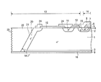
図1は、本発明の実施の形態1にかかる逆阻止型IGBTの構成を示す断面図である。図1に示すように、高比抵抗のn-シリコン半導体基板1の第1主面15に、pベース領域2が選択的に複数形成されている。基板裏面側の第2主面16には、p+コレクタ層3が形成されている。pベース領域2とp+コレクタ層3とによって基板厚さ方向に挟まれる領域は、もともとn-シリコン半導体基板1であり、nベース領域となる。特に限定しないが、n-シリコン半導体基板1の厚さ、すなわち第1主面15から第2主面16までの寸法は、例えば200μmである。
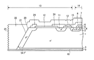
図3は、本発明の実施の形態2にかかる逆阻止型IGBTの構成を示す断面図である。図3に示すように、実施の形態2は、実施の形態1において、p+分離層20と切断面25との間の充填領域22が第1主面15上に伸びて、耐圧構造13および活性領域14を覆っているものである。その他の構成は、実施の形態1と同じである。従って、実施の形態1と同様に、p+分離層20によって、逆バイアス時にpn接合の前後に広がる空乏層が切断面25およびその周辺のダメージ領域に広がるのを防ぐことができるので、十分な逆耐圧を得ることができる。なお、実施の形態1と同様の構成については、実施の形態1と同じ符号を付して説明を省略する。
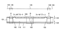
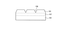
図10は、この発明の半導体装置(ここでは、逆阻止型IGBT)の半導体チップ形成箇所が多数集積した薄い半導体ウェハの構成を示す平面図である。図11は、図10のC−C線で切断した要部断面図であり、図12は、図11のD部とE部を拡大した図である。この薄い半導体ウェハは第1主面に表面構造が形成された厚い半導体ウェハの第2主面を研削し、この第2主面に裏面構造を形成した状態を示しており、スクライブラインとなるトレンチとこのトレンチに形成される分離層はまだ形成されていない状態を示す。
図22は、本発明の実施の形態4の逆阻止型IGBTの製造方法を示す要部断面図である。この断面図は、図17に相当する断面図である。図22に示すように、実施の形態4が実施の形態3と異なるのは、分離層145を形成するために、イオン注入後、低温アニールではなくレーザーアニール147を行うことである。その他のプロセスは、実施の形態3と同じである。なお、実施の形態3と同様の構成については、実施の形態3と同じ符号を付して説明を省略する。
図26および図27は、本発明の実施の形態5の逆阻止型IGBTの製造方法を順に示す要部断面図である。図26および図27に示すように、実施の形態5は、実施の形態4において、分離層145を形成した後、レーザー照射によるダイシング(レーザーダイシング)148を行ってトレンチ底面のpコレクタ領域110とコレクタ電極111を切断してから、発泡テープ138を加熱して薄い半導体ウェハ101を両面粘着テープ137から離すようにしたものである。その他のプロセスは、実施の形態4と同じである。なお、実施の形態4と同様の構成については、実施の形態3と同じ符号を付して説明を省略する。
2 第2導電型ベース領域(pベース領域)
3 第2導電型コレクタ層(p+コレクタ層)
4 第1導電型エミッタ領域(n+エミッタ領域)
5 ゲート絶縁膜
6 ゲート電極
8 エミッタ電極
9 コレクタ電極
15,131 第1主面
16,132,132a 第2主面
20 第2導電型分離層(p+分離層)
21,142 溝(トレンチ)
22 充填領域
31 シリコンウェハ
32 エッチングマスク
33,34 {100}面
35,36,37,38 {111}面
101 薄い半導体ウェハ
101a 厚い半導体ウェハ
102,103,104,110 拡散層(pウェル領域、p耐圧領域、nエミッタ領域、pコレクタ領域)
106 制御電極(ゲート電極)
108 第1主電極(エミッタ電極)
111 第2主電極(コレクタ電極)
137 接着層(両面粘着テープ)
138 発泡テープ
141 支持基板
143 側壁面
145 分離層
147 レーザーアニール
148 レーザーダイシング
Claims (5)
- 第1導電型半導体基板の第1主面の表面領域に選択的に設けられた第2導電型ベース領域と、前記ベース領域の表面領域に選択的に設けられた第1導電型エミッタ領域と、前記ベース領域の、前記半導体基板と前記エミッタ領域に挟まれた部分の表面上に設けられたゲート絶縁膜、および該ゲート絶縁膜上に設けられたゲート電極を含むMOSゲート構造と、前記エミッタ領域および前記ベース領域に接触するエミッタ電極と、前記半導体基板の第2主面の表面層に設けられた第2導電型コレクタ層と、前記コレクタ層に接触するコレクタ電極と、前記MOSゲート構造を囲み、かつ前記第1主面から前記第2主面に対して傾斜して前記第2主面まで至り、前記コレクタ層に連結された第2導電型分離層と、を有し、前記第1主面および前記第2主面は、{100}面であり、前記半導体基板に形成された溝の側壁は、{111}面である半導体装置を製造するにあたって、
第1導電型半導体基板の第1主面を所望のパターンのマスクで被覆する工程と、
前記半導体基板の、前記マスクにより被覆されていない部分をアルカリ溶液に接触させて湿式異方性エッチングを行い、前記半導体基板に、断面形状がV字状または台形状である溝を形成する工程と、
前記溝の側壁に第2導電型不純物を導入して第2導電型分離層を形成する工程と、
を含み、
前記溝の側壁に第2導電型不純物を導入した後に、前記第1主面に半導体膜を堆積して前記溝を当該半導体膜で埋め、その後に熱処理を行うことを特徴とする半導体装置の製造方法。 - 前記溝は、54.7°の角度で傾斜するよう形成し、前記側壁にイオン注入法により第2導電型不純物を導入することを特徴とする請求項1に記載の半導体装置の製造方法。
- 前記第1主面側にゲート絶縁膜およびゲート電極を含むMOSゲート構造を形成した後に、前記溝の形成と第2導電型不純物の導入を順次行って前記第2導電型分離層を形成することを特徴とする請求項1または2に記載の半導体装置の製造方法。
- 前記第1主面側にゲート絶縁膜およびゲート電極を含むMOSゲート構造を形成し、エミッタ電極を形成した後に、前記溝の形成と第2導電型不純物の導入を順次行って前記第2導電型分離層を形成することを特徴とする請求項1または2に記載の半導体装置の製造方法。
- 前記第1主面側にゲート絶縁膜およびゲート電極を含むMOSゲート構造を形成し、エミッタ電極を形成し、前記第1主面側の表面保護膜を形成した後に、前記溝の形成と第2導電型不純物の導入を順次行って前記第2導電型分離層を形成することを特徴とする請求項1または2に記載の半導体装置の製造方法。
Priority Applications (9)
| Application Number | Priority Date | Filing Date | Title |
|---|---|---|---|
| JP2005017486A JP4982948B2 (ja) | 2004-08-19 | 2005-01-25 | 半導体装置の製造方法 |
| DE102005038152A DE102005038152A1 (de) | 2004-08-19 | 2005-08-12 | Halbleiterbauteil und Verfahren zu seiner Herstellung |
| US11/208,459 US7741192B2 (en) | 2004-08-19 | 2005-08-19 | Semiconductor device and manufacturing method thereof |
| US11/389,495 US7776672B2 (en) | 2004-08-19 | 2006-03-27 | Semiconductor device and manufacturing method thereof |
| US12/575,730 US8697558B2 (en) | 2004-08-19 | 2009-10-08 | Semiconductor device and manufacturing method thereof |
| US12/785,932 US8119496B2 (en) | 2004-08-19 | 2010-05-24 | Semiconductor device and manufacturing method thereof |
| US12/824,541 US8759870B2 (en) | 2004-08-19 | 2010-06-28 | Semiconductor device |
| US13/352,581 US20120184083A1 (en) | 2004-08-19 | 2012-01-18 | Semiconductor device and manufacturing method thereof |
| US14/338,140 US20140327041A1 (en) | 2004-08-19 | 2014-07-22 | Semiconductor device and manufacturing method thereof |
Applications Claiming Priority (5)
| Application Number | Priority Date | Filing Date | Title |
|---|---|---|---|
| JP2004240094 | 2004-08-19 | ||
| JP2004240094 | 2004-08-19 | ||
| JP2004312590 | 2004-10-27 | ||
| JP2004312590 | 2004-10-27 | ||
| JP2005017486A JP4982948B2 (ja) | 2004-08-19 | 2005-01-25 | 半導体装置の製造方法 |
Related Child Applications (1)
| Application Number | Title | Priority Date | Filing Date |
|---|---|---|---|
| JP2011266344A Division JP5382098B2 (ja) | 2004-08-19 | 2011-12-05 | 半導体装置の製造方法 |
Publications (2)
| Publication Number | Publication Date |
|---|---|
| JP2006156926A JP2006156926A (ja) | 2006-06-15 |
| JP4982948B2 true JP4982948B2 (ja) | 2012-07-25 |
Family
ID=35852697
Family Applications (1)
| Application Number | Title | Priority Date | Filing Date |
|---|---|---|---|
| JP2005017486A Expired - Fee Related JP4982948B2 (ja) | 2004-08-19 | 2005-01-25 | 半導体装置の製造方法 |
Country Status (3)
| Country | Link |
|---|---|
| US (4) | US7741192B2 (ja) |
| JP (1) | JP4982948B2 (ja) |
| DE (1) | DE102005038152A1 (ja) |
Cited By (1)
| Publication number | Priority date | Publication date | Assignee | Title |
|---|---|---|---|---|
| WO2021096067A1 (ko) * | 2019-11-14 | 2021-05-20 | (주)오이솔루션 | 반도체 웨이퍼를 가공하기 위한 방법 |
Families Citing this family (60)
| Publication number | Priority date | Publication date | Assignee | Title |
|---|---|---|---|---|
| US7776672B2 (en) * | 2004-08-19 | 2010-08-17 | Fuji Electric Systems Co., Ltd. | Semiconductor device and manufacturing method thereof |
| JP4982948B2 (ja) * | 2004-08-19 | 2012-07-25 | 富士電機株式会社 | 半導体装置の製造方法 |
| JP5188673B2 (ja) * | 2005-06-09 | 2013-04-24 | 株式会社Sumco | Igbt用のシリコンウェーハ及びその製造方法 |
| DE102006007053B4 (de) | 2006-02-15 | 2008-08-14 | Infineon Technologies Austria Ag | Optimierte dielektrische Isolationsstrukturen und Verfahren zu deren Herstellung |
| JP4760729B2 (ja) * | 2006-02-21 | 2011-08-31 | 株式会社Sumco | Igbt用のシリコン単結晶ウェーハ及びigbt用のシリコン単結晶ウェーハの製造方法 |
| TWI354382B (en) * | 2007-06-01 | 2011-12-11 | Huga Optotech Inc | Semiconductor substrate with electromagnetic-wave- |
| JP5074172B2 (ja) | 2007-12-21 | 2012-11-14 | オンセミコンダクター・トレーディング・リミテッド | メサ型半導体装置及びその製造方法 |
| JP2009158589A (ja) | 2007-12-25 | 2009-07-16 | Sanyo Electric Co Ltd | メサ型半導体装置及びその製造方法 |
| TW200933899A (en) | 2008-01-29 | 2009-08-01 | Sanyo Electric Co | Mesa type semiconductor device and method for making the same |
| WO2009139417A1 (ja) * | 2008-05-13 | 2009-11-19 | 富士電機デバイステクノロジー株式会社 | 半導体装置およびその製造方法 |
| JP2010028018A (ja) * | 2008-07-24 | 2010-02-04 | Fuji Electric Device Technology Co Ltd | 半導体ウエハおよび半導体装置と半導体装置の製造方法 |
| JP5507118B2 (ja) * | 2009-05-20 | 2014-05-28 | 富士電機株式会社 | 半導体装置およびその製造方法 |
| JP5621271B2 (ja) * | 2010-02-12 | 2014-11-12 | 富士電機株式会社 | 逆阻止形絶縁ゲート型バイポーラトランジスタの製造方法 |
| JP2011187916A (ja) * | 2010-02-12 | 2011-09-22 | Fuji Electric Co Ltd | 逆阻止型絶縁ゲートバイポーラトランジスタの製造方法 |
| JP5740820B2 (ja) * | 2010-03-02 | 2015-07-01 | 富士電機株式会社 | 半導体装置および半導体装置の製造方法 |
| US8278690B2 (en) * | 2010-04-27 | 2012-10-02 | Omnivision Technologies, Inc. | Laser anneal for image sensors |
| JP5195816B2 (ja) | 2010-05-17 | 2013-05-15 | 富士電機株式会社 | 半導体装置の製造方法 |
| JP5621334B2 (ja) | 2010-06-10 | 2014-11-12 | 富士電機株式会社 | 半導体装置および半導体装置の製造方法 |
| JP2011257317A (ja) | 2010-06-10 | 2011-12-22 | Shinagawa Corp | 自動整準台 |
| JP5648379B2 (ja) * | 2010-06-14 | 2015-01-07 | 富士電機株式会社 | 半導体装置の製造方法 |
| JP5605032B2 (ja) * | 2010-07-09 | 2014-10-15 | 豊田合成株式会社 | 発光ダイオードの製造方法、切断方法及び発光ダイオード |
| JP5614451B2 (ja) | 2010-08-12 | 2014-10-29 | 富士電機株式会社 | 半導体装置の製造方法 |
| JP5549532B2 (ja) * | 2010-10-21 | 2014-07-16 | 富士電機株式会社 | 半導体装置の製造方法 |
| JPWO2012056536A1 (ja) | 2010-10-27 | 2014-03-20 | 富士電機株式会社 | 半導体装置および半導体装置の製造方法 |
| US8853009B2 (en) | 2011-01-18 | 2014-10-07 | Fuji Electric Co., Ltd. | Method for manufacturing reverse-blocking semiconductor element |
| JP5766462B2 (ja) * | 2011-02-24 | 2015-08-19 | ローム株式会社 | 半導体装置およびその製造方法 |
| US8999768B2 (en) | 2011-03-14 | 2015-04-07 | Fuji Electric Co., Ltd. | Semiconductor device manufacturing method |
| US9093266B2 (en) * | 2011-04-11 | 2015-07-28 | Micron Technology, Inc. | Forming high aspect ratio isolation structures |
| JP5866827B2 (ja) * | 2011-06-30 | 2016-02-24 | 富士電機株式会社 | 逆阻止型絶縁ゲート型バイポーラトランジスタの製造方法 |
| JP5929063B2 (ja) * | 2011-09-15 | 2016-06-01 | 富士電機株式会社 | 半導体装置の製造方法 |
| CN103384910B (zh) | 2012-02-23 | 2017-05-24 | 富士电机株式会社 | 半导体器件的制造方法 |
| US9981844B2 (en) | 2012-03-08 | 2018-05-29 | Infineon Technologies Ag | Method of manufacturing semiconductor device with glass pieces |
| US9219020B2 (en) | 2012-03-08 | 2015-12-22 | Infineon Technologies Ag | Semiconductor device, wafer assembly and methods of manufacturing wafer assemblies and semiconductor devices |
| JP5772670B2 (ja) * | 2012-03-12 | 2015-09-02 | 富士電機株式会社 | 逆阻止型半導体素子の製造方法 |
| JPWO2013176037A1 (ja) | 2012-05-22 | 2016-01-12 | 富士電機株式会社 | 半導体装置の製造方法 |
| JP6135666B2 (ja) | 2012-05-31 | 2017-05-31 | 富士電機株式会社 | 半導体装置の製造方法 |
| US9082808B2 (en) * | 2012-06-05 | 2015-07-14 | Oracle International Corporation | Batch process for three-dimensional integration |
| US8969177B2 (en) * | 2012-06-29 | 2015-03-03 | Applied Materials, Inc. | Laser and plasma etch wafer dicing with a double sided UV-curable adhesive film |
| RU2509391C1 (ru) * | 2012-09-21 | 2014-03-10 | Федеральное государственное бюджетное учреждение науки Институт физики полупроводников им. А.В. Ржанова Сибирского отделения Российской академии наук (ИФП СО РАН) | Способ формирования граней чипа для мозаичных фотоприемных модулей |
| EP2913843A4 (en) | 2012-10-23 | 2016-06-29 | Fuji Electric Co Ltd | METHOD FOR PRODUCING A SEMICONDUCTOR COMPONENT |
| JP5991384B2 (ja) * | 2013-01-16 | 2016-09-14 | 富士電機株式会社 | 半導体装置および半導体装置の製造方法 |
| US8859361B1 (en) * | 2013-04-05 | 2014-10-14 | Alpha And Omega Semiconductor Incorporated | Symmetric blocking transient voltage suppressor (TVS) using bipolar NPN and PNP transistor base snatch |
| CN104332494B (zh) * | 2013-07-22 | 2018-09-21 | 无锡华润上华科技有限公司 | 一种绝缘栅双极晶体管及其制造方法 |
| JP6036603B2 (ja) | 2013-08-21 | 2016-11-30 | 住友電気工業株式会社 | 炭化珪素半導体装置の製造方法 |
| FR3011124A1 (fr) * | 2013-09-26 | 2015-03-27 | St Microelectronics Tours Sas | Composant scr a caracteristiques stables en temperature |
| JP6320799B2 (ja) * | 2014-03-07 | 2018-05-09 | 住友重機械工業株式会社 | 半導体装置の製造方法 |
| US9570542B2 (en) | 2014-04-01 | 2017-02-14 | Infineon Technologies Ag | Semiconductor device including a vertical edge termination structure and method of manufacturing |
| JP6238234B2 (ja) * | 2014-06-03 | 2017-11-29 | ルネサスエレクトロニクス株式会社 | 半導体装置 |
| CN105448971B (zh) * | 2014-09-01 | 2019-04-09 | 中芯国际集成电路制造(上海)有限公司 | 一种半导体器件及其制作方法和电子装置 |
| CN106711036A (zh) * | 2015-11-12 | 2017-05-24 | 上海联星电子有限公司 | 逆阻型igbt芯片及其制作方法 |
| US11037904B2 (en) * | 2015-11-24 | 2021-06-15 | Taiwan Semiconductor Manufacturing Company, Ltd. | Singulation and bonding methods and structures formed thereby |
| JP6476419B2 (ja) * | 2016-02-04 | 2019-03-06 | パナソニックIpマネジメント株式会社 | 素子チップの製造方法および素子チップ |
| US9941256B1 (en) | 2016-12-21 | 2018-04-10 | Ixys Corporation | Inverse diode stack |
| JP6940302B2 (ja) * | 2017-05-25 | 2021-09-22 | レーザーテック株式会社 | 欠陥検査装置及び欠陥検査方法 |
| JP7175159B2 (ja) * | 2018-11-05 | 2022-11-18 | ソニーセミコンダクタソリューションズ株式会社 | 撮像素子および製造方法、並びに電子機器 |
| CN111261710A (zh) * | 2018-12-03 | 2020-06-09 | 珠海格力电器股份有限公司 | 一种绝缘栅双极型晶体管及其制备方法 |
| CN109961057B (zh) * | 2019-04-03 | 2021-09-03 | 罗克佳华科技集团股份有限公司 | 一种车辆位置获得方法及装置 |
| JP2022121327A (ja) * | 2021-02-08 | 2022-08-19 | 富士電機株式会社 | 炭化珪素半導体装置および炭化珪素半導体装置の製造方法 |
| CN118412367A (zh) * | 2023-01-30 | 2024-07-30 | 力特半导体(无锡)有限公司 | 用于半导体器件制造的玻璃沉积的方法 |
| CN118329124B (zh) * | 2024-06-07 | 2024-08-13 | 中国科学院海洋研究所 | 一种温度和电导率同测传感器制备方法及传感器 |
Family Cites Families (20)
| Publication number | Priority date | Publication date | Assignee | Title |
|---|---|---|---|---|
| JPS5269587A (en) * | 1975-12-08 | 1977-06-09 | Hitachi Ltd | Device and manufacture for high voltage resisting semiconductor |
| US4278987A (en) * | 1977-10-17 | 1981-07-14 | Hitachi, Ltd. | Junction isolated IC with thick EPI portion having sides at least 20 degrees from (110) orientations |
| US5332920A (en) * | 1988-02-08 | 1994-07-26 | Kabushiki Kaisha Toshiba | Dielectrically isolated high and low voltage substrate regions |
| US4904609A (en) | 1988-05-06 | 1990-02-27 | General Electric Company | Method of making symmetrical blocking high voltage breakdown semiconductor device |
| DE4340590A1 (de) * | 1992-12-03 | 1994-06-09 | Hewlett Packard Co | Grabenisolation unter Verwendung dotierter Seitenwände |
| JPH06252259A (ja) * | 1993-02-26 | 1994-09-09 | Ricoh Co Ltd | 半導体装置とその製造方法 |
| JPH09246371A (ja) * | 1996-03-14 | 1997-09-19 | Matsushita Electric Works Ltd | 半導体装置及びその製造方法 |
| JPH1064855A (ja) * | 1996-08-14 | 1998-03-06 | Toshiba Corp | 半導体装置の製造方法 |
| JP4131752B2 (ja) | 1997-03-14 | 2008-08-13 | 東芝松下ディスプレイテクノロジー株式会社 | 多結晶半導体膜の製造方法 |
| US6096656A (en) * | 1999-06-24 | 2000-08-01 | Sandia Corporation | Formation of microchannels from low-temperature plasma-deposited silicon oxynitride |
| JP4696337B2 (ja) * | 1999-10-15 | 2011-06-08 | 富士電機システムズ株式会社 | 半導体装置 |
| JP2001144213A (ja) * | 1999-11-16 | 2001-05-25 | Hitachi Ltd | 半導体装置の製造方法および半導体装置 |
| JP4788028B2 (ja) | 2000-08-28 | 2011-10-05 | 富士電機株式会社 | 逆阻止型igbtを逆並列に接続した双方向igbt |
| US6517546B2 (en) * | 2001-03-13 | 2003-02-11 | Gregory R. Whittaker | Method and apparatus for fixing a graft in a bone tunnel |
| US6920267B2 (en) * | 2002-05-13 | 2005-07-19 | Alps Electric Co., Ltd | Optical coupling device and manufacturing method thereof |
| JP4459571B2 (ja) | 2003-08-15 | 2010-04-28 | 株式会社半導体エネルギー研究所 | 半導体装置の作製方法 |
| US6897118B1 (en) * | 2004-02-11 | 2005-05-24 | Chartered Semiconductor Manufacturing Ltd. | Method of multiple pulse laser annealing to activate ultra-shallow junctions |
| JP4770140B2 (ja) | 2004-08-17 | 2011-09-14 | 富士電機株式会社 | 半導体素子の製造方法 |
| JP4982948B2 (ja) * | 2004-08-19 | 2012-07-25 | 富士電機株式会社 | 半導体装置の製造方法 |
| US7776672B2 (en) * | 2004-08-19 | 2010-08-17 | Fuji Electric Systems Co., Ltd. | Semiconductor device and manufacturing method thereof |
-
2005
- 2005-01-25 JP JP2005017486A patent/JP4982948B2/ja not_active Expired - Fee Related
- 2005-08-12 DE DE102005038152A patent/DE102005038152A1/de not_active Withdrawn
- 2005-08-19 US US11/208,459 patent/US7741192B2/en not_active Expired - Fee Related
-
2010
- 2010-05-24 US US12/785,932 patent/US8119496B2/en not_active Expired - Fee Related
-
2012
- 2012-01-18 US US13/352,581 patent/US20120184083A1/en not_active Abandoned
-
2014
- 2014-07-22 US US14/338,140 patent/US20140327041A1/en not_active Abandoned
Cited By (3)
| Publication number | Priority date | Publication date | Assignee | Title |
|---|---|---|---|---|
| WO2021096067A1 (ko) * | 2019-11-14 | 2021-05-20 | (주)오이솔루션 | 반도체 웨이퍼를 가공하기 위한 방법 |
| KR20210059151A (ko) * | 2019-11-14 | 2021-05-25 | 주식회사 오이솔루션 | 반도체 웨이퍼를 가공하기 위한 방법 |
| KR102366381B1 (ko) | 2019-11-14 | 2022-02-25 | 주식회사 오이솔루션 | 반도체 웨이퍼를 가공하기 위한 방법 |
Also Published As
| Publication number | Publication date |
|---|---|
| US8119496B2 (en) | 2012-02-21 |
| US7741192B2 (en) | 2010-06-22 |
| DE102005038152A1 (de) | 2006-03-09 |
| US20140327041A1 (en) | 2014-11-06 |
| US20060038206A1 (en) | 2006-02-23 |
| US20110081752A1 (en) | 2011-04-07 |
| JP2006156926A (ja) | 2006-06-15 |
| US20120184083A1 (en) | 2012-07-19 |
Similar Documents
| Publication | Publication Date | Title |
|---|---|---|
| JP4982948B2 (ja) | 半導体装置の製造方法 | |
| JP5082211B2 (ja) | 半導体装置の製造方法 | |
| US8759870B2 (en) | Semiconductor device | |
| US8507327B2 (en) | Semiconductor device manufacturing method thereof | |
| JP5614451B2 (ja) | 半導体装置の製造方法 | |
| JP5655931B2 (ja) | 半導体装置の製造方法 | |
| JP4231387B2 (ja) | 半導体装置とその製造方法 | |
| JP5358960B2 (ja) | 半導体装置およびその製造方法 | |
| JP5866827B2 (ja) | 逆阻止型絶縁ゲート型バイポーラトランジスタの製造方法 | |
| JP2011187916A (ja) | 逆阻止型絶縁ゲートバイポーラトランジスタの製造方法 | |
| JP5549532B2 (ja) | 半導体装置の製造方法 | |
| JP4857578B2 (ja) | 半導体装置の製造方法 | |
| KR20020053713A (ko) | 반도체장치 | |
| JP5382098B2 (ja) | 半導体装置の製造方法 | |
| JP2013239600A (ja) | 半導体装置の製造方法および半導体製造装置 | |
| JP5692241B2 (ja) | 逆阻止型半導体素子の製造方法 | |
| JP2005175174A (ja) | 絶縁ゲート型バイポーラトランジスタの製造方法 | |
| JP4572529B2 (ja) | 半導体素子の製造方法 | |
| JP2009206285A (ja) | 半導体装置の製造方法および半導体装置 | |
| JP2014143435A (ja) | 半導体装置 |
Legal Events
| Date | Code | Title | Description |
|---|---|---|---|
| A625 | Written request for application examination (by other person) |
Free format text: JAPANESE INTERMEDIATE CODE: A625 Effective date: 20071213 |
|
| A711 | Notification of change in applicant |
Free format text: JAPANESE INTERMEDIATE CODE: A711 Effective date: 20080204 |
|
| RD03 | Notification of appointment of power of attorney |
Free format text: JAPANESE INTERMEDIATE CODE: A7423 Effective date: 20080204 |
|
| RD04 | Notification of resignation of power of attorney |
Free format text: JAPANESE INTERMEDIATE CODE: A7424 Effective date: 20080205 |
|
| A711 | Notification of change in applicant |
Free format text: JAPANESE INTERMEDIATE CODE: A712 Effective date: 20091112 |
|
| RD03 | Notification of appointment of power of attorney |
Free format text: JAPANESE INTERMEDIATE CODE: A7423 Effective date: 20091112 |
|
| RD04 | Notification of resignation of power of attorney |
Free format text: JAPANESE INTERMEDIATE CODE: A7424 Effective date: 20091112 |
|
| A711 | Notification of change in applicant |
Free format text: JAPANESE INTERMEDIATE CODE: A712 Effective date: 20110422 |
|
| A977 | Report on retrieval |
Free format text: JAPANESE INTERMEDIATE CODE: A971007 Effective date: 20110926 |
|
| A131 | Notification of reasons for refusal |
Free format text: JAPANESE INTERMEDIATE CODE: A131 Effective date: 20111004 |
|
| A521 | Request for written amendment filed |
Free format text: JAPANESE INTERMEDIATE CODE: A523 Effective date: 20111205 |
|
| A131 | Notification of reasons for refusal |
Free format text: JAPANESE INTERMEDIATE CODE: A131 Effective date: 20111227 |
|
| A521 | Request for written amendment filed |
Free format text: JAPANESE INTERMEDIATE CODE: A523 Effective date: 20120227 |
|
| TRDD | Decision of grant or rejection written | ||
| A01 | Written decision to grant a patent or to grant a registration (utility model) |
Free format text: JAPANESE INTERMEDIATE CODE: A01 Effective date: 20120327 |
|
| A01 | Written decision to grant a patent or to grant a registration (utility model) |
Free format text: JAPANESE INTERMEDIATE CODE: A01 |
|
| A61 | First payment of annual fees (during grant procedure) |
Free format text: JAPANESE INTERMEDIATE CODE: A61 Effective date: 20120409 |
|
| R150 | Certificate of patent or registration of utility model |
Free format text: JAPANESE INTERMEDIATE CODE: R150 |
|
| FPAY | Renewal fee payment (event date is renewal date of database) |
Free format text: PAYMENT UNTIL: 20150511 Year of fee payment: 3 |
|
| LAPS | Cancellation because of no payment of annual fees |