JP4983355B2 - Temperature measuring method or electronic device temperature measuring apparatus - Google Patents
Temperature measuring method or electronic device temperature measuring apparatus Download PDFInfo
- Publication number
- JP4983355B2 JP4983355B2 JP2007103071A JP2007103071A JP4983355B2 JP 4983355 B2 JP4983355 B2 JP 4983355B2 JP 2007103071 A JP2007103071 A JP 2007103071A JP 2007103071 A JP2007103071 A JP 2007103071A JP 4983355 B2 JP4983355 B2 JP 4983355B2
- Authority
- JP
- Japan
- Prior art keywords
- temperature
- light
- electronic device
- sensitive material
- timing
- Prior art date
- Legal status (The legal status is an assumption and is not a legal conclusion. Google has not performed a legal analysis and makes no representation as to the accuracy of the status listed.)
- Expired - Fee Related
Links
Images





Landscapes
- Investigating, Analyzing Materials By Fluorescence Or Luminescence (AREA)
Description
電子デバイスなどの被測定物質の表面温度を非接触で精度良くかつ高速に測定する方法、装置に関する。 The present invention relates to a method and apparatus for measuring the surface temperature of a substance to be measured such as an electronic device with high accuracy and high speed without contact.
従来より被測定対象の表面温度を非接触で測定する技術が提案されており、例えば下記特許文献1では、蛍光強度が温度依存性を備える無機蛍光体を感温材料として用い、この感温材料を被測定物質の表面に被覆形成し、照射する励起光に対する無機蛍光体の蛍光発光強度を測定し、温度を求めている。
Conventionally, a technique for measuring the surface temperature of an object to be measured in a non-contact manner has been proposed. For example, in
また、特許文献2でも、被測定物質を蛍光体で被覆し、パルス光を照射し、照射後、蛍光強度を測定することを開示している。特許文献2では、さらに蛍光の減衰期の第1測定時刻、蛍光が存在(残存)している第2測定時刻に蛍光測定を実行し、第1測定時刻と第2測定時刻の蛍光強度の比率から表面温度を算出している。
特許文献3では、測定対象物に付着させる感温蛍光材料として、蛍光の発光効率の温度依存性が異なる2種類を混合する。この感温蛍光材料の付着された測定対象物に励起光源からの光を照射し、得られる蛍光像をCCDカメラで撮像する。そして、この撮像データから検出してその強度比から温度を算出する。特許文献3のように温度依存性の異なる2種類の蛍光材料を感温蛍光材料に採用することで、低温における2次元の温度分布をリアルタイムで画像化することを提案している。
In
ディスプレイや半導体装置などの電子デバイスにおいては、電気信号によって高速駆動が行われており、その信頼性評価の一環として熱解析が必要とされる。しかし、上記特許文献1,2,3等に示されるような温度測定装置では、温度測定精度を向上させたり、2次元画像による温度分布の測定等の空間分解能の向上を目的としており、被測定対象の温度変化について、その時間分解能についての認識がなかった。
Electronic devices such as displays and semiconductor devices are driven at high speed by electrical signals, and thermal analysis is required as part of their reliability evaluation. However, the temperature measuring devices as shown in the above-mentioned
例えば、上記特許文献1では、被計測対象の表面温度を測定することしか記載がない。また、特許文献2では、パルス光の照射から10μsec経過した後に第1測定を実行し、パルス光照射から310μsec経過した後に第2測定を実行している。ところが、被計測対象を動作させるという認識も、被計測対象の動作タイミングとの相関関係を考慮することについての認識もない。
For example, the above-mentioned
さらに、特許文献3では、カラーCCDカメラを用いて発光強度を測定するため、1スキャン数十msec以上の測定時間が必要であり、時間分解はできない。
Furthermore, in
一方、高速な温度計測として、レーザ励起によるラマン散乱や蛍光を用いる方法が知られている。しかし、これらレーザ励起によるラマン散乱などを用いる測定装置は、非常に大がかりである。 On the other hand, as a high-speed temperature measurement, a method using Raman scattering or fluorescence by laser excitation is known. However, a measuring apparatus using such Raman scattering by laser excitation is very large.
このように、従来、簡便な装置構成で、msec程度の時間分解能を有し、また、経時的な温度変化についても観察容易な温度計測手法(装置)は存在しない。よって、パルス信号などによって駆動される電子デバイスに対しては、パルス駆動中ならびに駆動後の熱の過渡応答を簡便かつ高速応答可能な手法で測定することができず、熱電対などの応答性の悪い手法で定常状態の温度を計測するにとどまっていた。 Thus, conventionally, there is no temperature measurement method (apparatus) that has a simple apparatus configuration, has a time resolution of about msec, and that can easily observe temperature changes over time. Therefore, for electronic devices driven by pulse signals, etc., it is not possible to measure the transient response of heat during and after pulse driving with a simple and fast response technique. It was only measuring the steady state temperature with a bad technique.
本発明は、非接触で高い時間分解能の温度測定を実行する手段を提供する。 The present invention provides a means for performing non-contact, high time resolution temperature measurements.
本発明は、温度測定方法であり、被測定物体の表面を、発光特性が温度依存性を有する発光物質を含有する感温材料で被覆し、前記感温材料で被覆された前記被測定物体の動作タイミングに同期して、前記発光物質にパルス光を照射するためのタイミング制御を行い、前記被測定物体の動作タイミングから所定時間経過後にパルス光を照射し、前記被測定物体の動作タイミングに同期して、前記パルス光照射による前記発光物質の発光光を検知するためのタイミング制御を行い、前記パルス光照射によって前記感温材料から放出された光を受光し、受光光と、前記感温材料の発光特性の温度との関係に基づいて、前記被測定物体のパルス動作から所定タイミング経過時の前記被測定物体の表面温度を求める。 The present invention is a temperature measurement method, wherein a surface of an object to be measured is coated with a temperature-sensitive material containing a light-emitting substance whose emission characteristics have temperature dependence, and the object to be measured is coated with the temperature-sensitive material. In synchronization with the operation timing, the timing control for irradiating the light emitting material with pulsed light is performed, the pulsed light is irradiated after a predetermined time has elapsed from the operation timing of the measured object, and synchronized with the operation timing of the measured object. Then, timing control for detecting the emitted light of the luminescent material by the pulsed light irradiation is performed, the light emitted from the temperature sensitive material by the pulsed light irradiation is received, the received light, and the temperature sensitive material The surface temperature of the object to be measured when a predetermined timing elapses is obtained from the pulse operation of the object to be measured based on the relationship between the light emission characteristics and the temperature.
本発明の他の態様では、上記温度測定方法において、前記被測定物体は、電気的に駆動される電気デバイスであり、前記発光物質は蛍光物質を含み、該電気デバイスをパルス駆動し、該パルス駆動から所定時間が経過した後に、前記パルス光を照射し、前記電子デバイスのパルス駆動に同期して前記表面温度を計測するタイミングを制御し、前記電子デバイスのパルス駆動から所定時間経過後における前記電子デバイス温度を求める。 In another aspect of the present invention, in the temperature measurement method, the object to be measured is an electrically driven electric device, the luminescent material includes a fluorescent material, the electric device is pulse-driven, and the pulse After a predetermined time has elapsed from the drive, the pulsed light is irradiated, the timing of measuring the surface temperature in synchronization with the pulse drive of the electronic device is controlled, and the time after the predetermined time has elapsed from the pulse drive of the electronic device Determine the electronic device temperature.
本発明の他の態様では、上記温度測定方法において、前記電子デバイスに対する所定周波数での駆動と、該駆動から一定時間後の前記感温材料へのパルス光の照射と、前記感温材料から放出された光の計測と、を繰り返し実行し、計測結果の平均値に基づいて発光スペクトルからピーク波長を求め、表面温度を求める。 In another aspect of the present invention, in the temperature measurement method, the electronic device is driven at a predetermined frequency, the pulsed light is irradiated to the temperature-sensitive material after a predetermined time from the drive, and the temperature-sensitive material is emitted. The measurement of the measured light is repeatedly executed, the peak wavelength is obtained from the emission spectrum based on the average value of the measurement results, and the surface temperature is obtained.
本発明の他の態様では、電気信号により駆動可能な電子デバイスの表面に形成され、発光特性が温度依存性を有する発光物質を含有する感温材料層に対し、パルス光を照射して得られる発光光と、前記温度依存性とに基づいて、前記電子デバイスの表面温度を測定する装置であり、前記感温材料層で被覆した前記電子デバイスの表面に対してパルス光を照射する光源と、前記電子デバイスの電気的な駆動と同期させて、前記光源の発光タイミングの制御を実行し、前記電子デバイスの駆動タイミングから所定時間経過後に前記光源を発光させる光源制御部と、前記パルス光によって励起された感温材料層の発光光を検出する光検出部であって、前記電子デバイスの電気的な駆動と同期させて、光検出動作タイミングの制御を実行し、所定タイミングで光検出を行う光検出部と、を備え、前記電子デバイスの所定の駆動タイミングから所定時間経過後に、前記パルス光の照射に応じて前記感温材料層から得られた光と、前記発光物質の温度依存性とから前記電子デバイスの表面温度を算出する演算部と、を備える。 In another aspect of the present invention, a temperature-sensitive material layer that is formed on the surface of an electronic device that can be driven by an electric signal and that contains a light-emitting substance whose emission characteristics are temperature-dependent is obtained by irradiating pulsed light. An apparatus for measuring the surface temperature of the electronic device based on the emitted light and the temperature dependence, and a light source for irradiating the surface of the electronic device covered with the temperature-sensitive material layer with pulsed light, A light source controller that controls the light emission timing of the light source in synchronization with the electrical drive of the electronic device and emits the light source after a lapse of a predetermined time from the drive timing of the electronic device, and excited by the pulsed light A light detection unit for detecting the emitted light of the temperature-sensitive material layer, wherein the light detection operation timing is controlled in synchronization with an electrical drive of the electronic device, and a predetermined type is detected. A light detection unit that performs light detection at a time, and after a predetermined time has elapsed from a predetermined drive timing of the electronic device, the light obtained from the temperature-sensitive material layer according to the irradiation of the pulsed light, and the light emission A calculation unit that calculates the surface temperature of the electronic device from the temperature dependence of the substance.
本発明の他の態様では、上記電子デバイスの温度測定装置において、前記光源制御部は、前記電子デバイスに印加される駆動パルス信号に同期した信号を一定期間遅延させる遅延回路を備え、該遅延回路によって遅延された前記駆動パルス信号に同期した信号に応じたタイミングで前記光源を発光させ、前記光検出部は、前記電子デバイスに印加される駆動パルス信号に同期した信号を一定期間遅延させる遅延回路を備え、該遅延回路によって遅延された前記駆動パルス信号に同期した信号に応じたタイミングで前記感温材料層から得た光の検出を実行する。 In another aspect of the present invention, in the temperature measuring apparatus for an electronic device, the light source control unit includes a delay circuit that delays a signal synchronized with a drive pulse signal applied to the electronic device for a predetermined period, and the delay circuit A delay circuit for causing the light source to emit light at a timing according to a signal synchronized with the drive pulse signal delayed by the delay, and for delaying a signal synchronized with the drive pulse signal applied to the electronic device by a predetermined period. And detecting light obtained from the temperature-sensitive material layer at a timing corresponding to a signal synchronized with the drive pulse signal delayed by the delay circuit.
本発明の他の態様では、上記装置において、前記光源は、紫外発光ダイオードを備えるパルス励起光源であり、前記光検出部は、複数の波長域を検出するマルチチャンネル検出器を備える。 In another aspect of the present invention, in the above device, the light source is a pulse excitation light source including an ultraviolet light emitting diode, and the light detection unit includes a multichannel detector that detects a plurality of wavelength regions.
本発明の他の態様では、上記方法又は装置において、前記発光物質は、無機発光体又は有機発光体である。また、前記発光物質は、酸化物又は硫化物又は硫化酸化物に、希土類又は貴金属が添加された無機蛍光体、または、ルテニウムビピリジン錯体、アミノ基を有するアミノベンゼン誘導体、アミノナフタレン誘導体、アミノフタレイン誘導体のいずれかの有機蛍光体を採用することも可能である。 In another aspect of the present invention, in the above method or apparatus, the luminescent material is an inorganic luminescent material or an organic luminescent material. The light-emitting substance is an inorganic phosphor obtained by adding a rare earth or noble metal to an oxide, sulfide, or sulfide oxide, or a ruthenium bipyridine complex, an aminobenzene derivative having an amino group, an aminonaphthalene derivative, an aminophthalein. It is also possible to employ any organic phosphor of a derivative.
本発明は、感温材料に採用する発光物質として、その発光スペクトルのピーク波長やピーク強度等のいわゆる発光特性が、温度依存性を有する材料を用い、被測定物体の動作タイミングに基づいて、発光物質を含む感温材料を被覆した被測定物体へのパルス光照射タイミングを制御する。よって、被測定物体の動作タイミングから所定時間経過後の光の検知結果を得ることができる。このため、被測定物体の動作からその表面温度の過渡的な変化を測定することができる。 The present invention employs a material whose so-called emission characteristics such as peak wavelength and peak intensity of the emission spectrum are temperature-dependent as the luminescent substance employed in the temperature-sensitive material, and emits light based on the operation timing of the object to be measured. The pulsed light irradiation timing to the object to be measured coated with the temperature sensitive material containing the substance is controlled. Therefore, it is possible to obtain a light detection result after a predetermined time has elapsed from the operation timing of the object to be measured. For this reason, a transient change in the surface temperature can be measured from the operation of the object to be measured.
以下、図面を参照して本発明の実施の形態(以下、実施形態)について説明する。 Embodiments (hereinafter, embodiments) of the present invention will be described below with reference to the drawings.
図1は、本実施形態に係る温度計測装置の概略構成図を示している。この装置では、発光特性が温度依存性を有する発光物質を含有する感温材料層110が、被測定物体100の表面に形成されている。この被測定物体100に対し、光源制御部310によって発光タイミングが制御される光源312からパルス光が照射され、パルス光照射によって得られる発光を受光部332を介して光検出部330が検出する。演算部350は、受光結果とその発光物質の温度依存性とに基づいて、被測定物体の表面温度を求める。
FIG. 1 shows a schematic configuration diagram of a temperature measuring apparatus according to the present embodiment. In this apparatus, a temperature-
制御部370は、被測定物体100の駆動タイミングに応じて、発光タイミングの制御及び光検出タイミングを制御するために、この被測定物体の駆動信号に同期した制御信号を光源制御部310、光検出部330に供給する。また演算部350に対してもこの制御信号を供給し、演算結果(温度測定結果)と被測定物体の動作タイミングとの対応付けをこの制御信号を利用して行っても良い。
In order to control the light emission timing and the light detection timing in accordance with the drive timing of the measured
被測定物体100は、本実施形態において、半導体装置や、ディスプレイなど、電気信号によって様々な動作をする電子デバイスであり、配線などにはパルス状の電気等がデバイス駆動部200から出力され、その電気信号に応じ、発光や光変調等を実行したり、導通して電流等を流したりする。このような電子デバイスは、その電気信号などに応じて配線や、ディスプレイの場合には画素部などにおいて、短時間で熱負荷がかかる。
In this embodiment, the
したがって、この熱負荷による熱現象の解析にあたり、制御部370は、電子デバイスに対するパルス信号と同期した制御信号を光源制御部310に供給し、光源制御部310は、この制御信号を内蔵する遅延回路によって定まる時刻だけ遅延させて光源駆動用パルス信号を発生し、光源312に供給する。
Therefore, in the analysis of the thermal phenomenon due to the thermal load, the
光源制御部310の遅延回路は、被測定物体の駆動から、例えばμsec〜sec程度の範囲で最低限測定する必要のある少なくとも1回のタイミングで光源駆動用パルス信号が出力されるように、少なくとも1種類の遅延時間(μsec〜sec)が設定される。また、温度の経時変化を観察する用途に対応する場合には、被駆動物体の動作からμsec〜secの範囲で複数時間設定できることが望ましい。なお、この遅延時間は、光源駆動用パルス信号に対する光源312の応答速度及び感温材料層110の発光応答速度等を考慮して決定することができる。
The delay circuit of the light
光源312は、光検出部330での検出が可能な程度に感温材料層110を励起することのできる波長、エネルギのパルス光を射出する光源(パルス励起光源)を備え、例えば高速応答の可能な紫外発光ダイオードが採用できる。また、この光源312は、光源制御部310から光源駆動用パルス信号が供給されたタイミングで発光する。さらに、光源312からのパルス光を局部的に照射し、その部分における温度を測定する場合には、図1に示すように、集光系レンズ314を採用し、光源312からの光をこの集光系レンズ314で集光し、測定目的領域に選択的に照射する。
The
受光部332は、感温材料層110の励起光を受光できる位置に配置され、光ファイバーを通じて受光信号を光検出部330へ伝える。光検出部330は、上記電子デバイスのパルス信号に同期して制御部370から供給される制御信号を、内蔵する遅延回路によって所定時刻だけ遅延させたタイミングから受光信号の検出を実行する。この遅延時間は、電子デバイス100を駆動するパルス信号に同期した制御信号に対する上記光源駆動用パルス信号の遅延時間と同じに設定することで、パルス光の照射と同時に光検出を実行することができる。
The
なお、この光検出部330での光検出タイミングの制御信号に対する遅延時間についても、光源駆動用パルス信号に対する光源312の応答速度及び感温材料層110の発光応答速度を考慮することができる。
Note that the response speed of the
ここで、上記光源312の発光タイミングと光検出タイミングを精度良く同期させるためには、光源制御部310の遅延回路と、光検出部330の遅延回路とを共用することが好適である。
Here, in order to accurately synchronize the light emission timing and the light detection timing of the
また、光検出部330において、常時、光検出処理を実行してもよく、その場合には、演算部350又はこの光検出部330において、電子デバイスへのパルス信号の印加タイミング又はパルス光の照射タイミングに基づいて、パルス光の照射タイミングからの検出信号を演算部350での演算対象にするように制御する(パルス光照射によって得られた光を正確に検出するためである)。
In addition, the
なお、光検出部330としては、マルチチャンネル検出器を採用することができ、これにより、感温材料層110の励起光の強度を複数の波長域について検出することができ、より正確にピーク強度を検出することができる。例えば、励起光として400nm以下の紫外線を発光させることのできる紫外LEDを上記光源312に採用し、CCDアレイ等を用いたマルチチャネル検出器を採用することで高速かつ正確なピーク波長又はピーク強度を測定することができる。
Note that a multi-channel detector can be employed as the
ここで、発光物質(例えば蛍光物質)の発光の減衰時間tdは、td<1msec、光源312として用いる紫外発光ダイオードの応答速度Vrは、Vr<1msecである。このように、感温材料として光の減衰時間が十分短く、かつ光源として応答速度が十分速いものを採用することで、msec単位の温度測定が可能となる。また、光源制御部310の発生する光源駆動用パルス信号の遅延時間Δtをμsec〜secの範囲で任意に設定することで、被測定物体100の駆動開始からmsec単位の熱の過渡現象を測定することが可能となる。ここで、遅延時間は、この光源制御部310に採用する遅延回路によって容易に設定することができる。このような構成の採用により、被測定物体の動作タイミングからmsec単位の温度の過渡現象を測定できる。
Here, the decay time td of light emission of the light emitting material (for example, fluorescent material) is td <1 msec, and the response speed Vr of the ultraviolet light emitting diode used as the
得られる蛍光の強度が弱い場合には、電子デバイスの駆動と同期している紫外発光ダイオードの駆動を電子デバイスの駆動と共に繰り返し実行し、光検出器による検出も対応して繰り返し実行し、各電子デバイス駆動時に得られた光検出信号を積算し、積算値から平均を演算して、精度の高い温度情報を得ることができる。 When the intensity of the obtained fluorescence is weak, the driving of the ultraviolet light-emitting diode synchronized with the driving of the electronic device is repeatedly executed together with the driving of the electronic device, and the detection by the photodetector is also repeatedly executed correspondingly. Accurate temperature information can be obtained by integrating the photodetection signals obtained when the device is driven and calculating an average from the integrated values.
なお、予め以上のような温度測定方法により得られる光検出信号と表面温度との関係を求めて検量線を作成して格納しておくことが好適である。実測定時には、得られた光検出信号又はその積算・平均値から上記検量線データを参照して、表面温度を求めることができ、正確、迅速に測定結果を得ることができる。上述のように、本実施形態では、数msecの時間分解能で表面の温度変化を発光物質のピーク波長から算出することができる。なお、ピーク強度が温度依存性を有する発光材料を感温材料に用いる場合には、光の強度(ピーク強度)を測定し、予め求めたピーク強度と温度との検量線を用いて温度を算出する。 It is preferable that a calibration curve is created and stored in advance by obtaining the relationship between the light detection signal obtained by the temperature measuring method as described above and the surface temperature. In actual measurement, the surface temperature can be obtained by referring to the calibration curve data from the obtained light detection signal or its integrated / average value, and the measurement result can be obtained accurately and quickly. As described above, in this embodiment, the temperature change of the surface can be calculated from the peak wavelength of the luminescent material with a time resolution of several milliseconds. When a light-emitting material whose peak intensity is temperature-dependent is used as a temperature-sensitive material, the intensity of light (peak intensity) is measured, and the temperature is calculated using a calibration curve between the peak intensity and temperature obtained in advance. To do.
図2は、被測定物体100として採用される電子デバイスの具体的な構成例を示している。この例では、電子デバイスとして有機EL素子10を採用している。有機EL素子10は、ガラスなどの基板12の上に、第1電極14,第2電極16が形成され、この第1電極14と第2電極16の間に有機発光材料を含む有機層20が形成されている。図2の例では、基板12側の第1電極14に、透明金属酸化物であるITO(Indium tin Oxide)等を用いた透明電極層を採用し、第2電極16としては、Al、Ag、MgAg等の金属層を採用している。有機層20は、採用する発光材料等の特性に応じ、単層でも多層でも良く、例えば、陽極側(本実施形態では、第1電極14)から、正孔輸送層、発光層の2層構造を採用している。なお、本実施形態では第2電極16を陰極として用いており、上記金属層と有機層20との間には電子注入層としてLiF等からなる薄い層が設けられている(上記金属層と電子注入層を一体的に第2電極16と表現することも可能である)。
FIG. 2 shows a specific configuration example of an electronic device employed as the
このようなEL素子は、有機層20に対し、陽極から正孔を、陰極から電子を注入し、有機層20中で正孔と電子が再結合し、その再結合エネルギにより有機発光材料が励起され、基底状態に戻る際に得られる光を表示や光源などに用いる。
Such an EL element injects holes from the anode and electrons from the cathode into the
図2の有機EL素子10では、基板12側の透明な第1電極14から基板12を介して外部に光が射出される。本実施形態に係る感温材料層110は、不透明な金属層からなる第2電極16を覆うように形成している。感温材料層110の形成された有機EL素子は、外来の水分や酸素による劣化を防止するために、封止部材30を基板12に接着することで、有機EL素子の形成領域をこの基板12と封止部30とによって外界から遮蔽している。有機EL素子の形成領域は、このような封止部材30によってその側方及び上方が取り囲まれ、封止空間32には、N2、Ar等の不活性気体(非酸化性気体)が封入されている。
In the
封止部材30として透明なガラスを採用することで、本実施形態に係る感温材料層110の形成された有機EL素子に対し、このEL素子を駆動し、これと同期して所定タイミングで、素子封止状態で封止部材30側から、パルス光を照射し、かつ、感温材料層110の発光を検知することができる。
By adopting transparent glass as the sealing
次に感温材料層110に採用する発光物質について説明する。
Next, the light emitting substance employed in the temperature
本実施形態において、発光物質に採用可能な物質としては、以下に示すような蛍光波長や蛍光強度の温度依存性の大きい無機物質や有機物質の蛍光物質が挙げられる。 In the present embodiment, examples of substances that can be employed as the light emitting substance include inorganic substances and organic substances that have a large temperature dependency of the fluorescence wavelength and fluorescence intensity as described below.
無機材料の例としては、酸化物や硫化物又は硫化酸化物に希土類や貴金属が添加された蛍光体を用いることができ、一例として、
La2O2S:Eu、YVO4:Eu、(Zn、Cd)S:Ag、ZnS:Ag、Cu、Ga、Cl、ZnS:Ag、ZnS:Cu、Al、Y2O3S:Eu
などを用いることができる。
As an example of an inorganic material, a phosphor in which a rare earth or a noble metal is added to an oxide, sulfide, or sulfide oxide can be used.
La 2 O 2 S: Eu, YVO 4 : Eu, (Zn, Cd) S: Ag, ZnS: Ag, Cu, Ga, Cl, ZnS: Ag, ZnS: Cu, Al, Y 2 O 3 S: Eu
Etc. can be used.
有機材料の例としては、重金属の錯体であるルテニウムビピリジン錯体(Ru(bpy)3)やアミノ基を有するアミノベンゼン誘導体、アミノナフタレン誘導体、アミノフタレイン誘導体などを用いることができる。 As an example of the organic material, a ruthenium bipyridine complex (Ru (bpy) 3 ) that is a complex of a heavy metal, an aminobenzene derivative having an amino group, an aminonaphthalene derivative, an aminophthalein derivative, or the like can be used.
なお、感温材料層110の厚さについては、特に制限はないが、層として安定して存在するために必要な厚さがあり、十分な励起エネルギーを光源312からの光から得るのに十分な厚さとすれば良く、一例として100nm程度とすることができる。なお、図2に示す有機EL素子において、上部側の第2電極16を透明電極とし、封止部材30側からEL素子の光を外部に取り出す構成の場合、感温材料層110は、通常のEL素子発光時において、その発光光を透過可能な材料を用いる。また、EL素子の通常動作時(発光時)にこのEL発光光によって感温材料層110が発光しないよう、感温材料としては、EL素子からの光では励起せず、光源312からの光によって選択的に励起されて発光する材料を採用することが好適である。
Note that the thickness of the temperature-
以上本実施形態では、電子デバイス100の駆動をパルス信号で実行し、また光源312についてもパルス信号で駆動してパルス波を発生させている。このようにパルス駆動としているのは、測定タイミングを明確化し、測定の精度を向上させる上で望ましい。但し、連続波(アナログ波)による電子デバイスの駆動、光源からの光が連続波である場合でも、デバイス駆動開始タイミング、発光開始タイミングを正確に制御することで温度測定の精度を維持することができる。
As described above, in the present embodiment, the
[実施例1]
(電子デバイスの作製)
電子デバイスとして上述の図2に示すような有機EL素子を用い、その素子の温度計測を実施した。
[Example 1]
(Production of electronic devices)
The organic EL element as shown in FIG. 2 was used as the electronic device, and the temperature of the element was measured.
ガラス基板12上にITO(インジュウム錫酸化物)の透明電極14を100nmの膜厚で形成しパターニング後、有機洗浄、純水洗浄、乾燥、UVオゾン処理を行った。その基板12を直ちに真空チャンバへ導入後、ArとO2のプラズマ処理を行った。
A
次に、真空蒸着(真空度7×10⁻⁵ Pa)により、下記式(1)

その後、発光層として、下記式(2)
このようにして有機EL素子を作製した後、Alの金属電極16上に蛍光ピークの温度依存性があることが知られている下記式(3)
このような素子部の形成された基板12を高純度の窒素ガスが循環しているグローブボックス内に搬送し、透明なガラスを封止部材30として用い、有機EL素子と感温材料層とを、紫外線硬化樹脂を用いて基板12上において封止した。
The
(電子デバイスの時間分解温度測定)
図1で示した光学式温度計測装置を用いて、電子デバイスとして上述の図2に例示する有機EL素子10の温度測定を実施した。作製した有機EL素子10の電極18(第1電極14及び第2電極16)に対し、30Hz、パルス幅0.5msec、電圧20Vのパルス信号を供給してパルス駆動した。このときの有機EL素子の平均輝度は、1600cd/m2であった。なお、この図1に例示するパルス波が定常レベルより高いパルス信号を、本実施例では、第1電極14とこれと有機層20を挟んで対向する第2電極16の陽極として機能する電極に印加し、他方の電極は一定電位に固定することで、有機層20に対し、上記パルス信号に応じた電流を流し、有機層20中に含まれる有機発光材料を発光させる。なお、有機層20を同様に発光させることができる他の方法としては、図1に示すパルス信号とは逆極性のパルス信号を陰極として機能する電極に印加しても良いし、陽極と陰極に対し、互いに逆極性で、かつ電圧の絶対値が上記20Vの半分のパルス信号をさせてもよい。
(Measurement of time-resolved temperature of electronic devices)
Using the optical temperature measuring device shown in FIG. 1, the temperature of the
この有機EL素子10への駆動パルス信号の印加から、任意の遅れ時間経過後、紫外発光ダイオードを0.5msecの間パルス駆動し、感温材料層110から射出される蛍光のスペクトルをマルチチャンネル検出器330により検出した。
After an arbitrary delay time has elapsed from the application of the drive pulse signal to the
検出は、暗箱内で実施しており、発光ダイオードからの紫外パルス光の照射によって感温材料が励起されている時間領域のみの蛍光スペクトルが得られる。光検出器330の感度に応じて、このようなEL素子の駆動、パルス光照射、及び測定を繰り返し、温度演算が容易にできるノイズの少ない信号を得るようにした。
Detection is carried out in a dark box, and a fluorescence spectrum only in the time domain in which the temperature-sensitive material is excited by irradiation with ultraviolet pulse light from the light emitting diode is obtained. According to the sensitivity of the
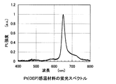
得られた蛍光スペクトルを図3に示す。なお、予め、恒温槽を用いて作成した蛍光ピーク波長と温度との関係を利用し、図4に示すような検量線を作成した。この検量線を用いて蛍光スペクトルのピーク波長から温度を算出した。 The obtained fluorescence spectrum is shown in FIG. In addition, the calibration curve as shown in FIG. 4 was created in advance using the relationship between the fluorescence peak wavelength and temperature created using a thermostat. Using this calibration curve, the temperature was calculated from the peak wavelength of the fluorescence spectrum.
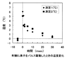
有機EL駆動から紫外の発光ダイオードの駆動時間との差である遅れ時間を変え、上記の測定を繰り返すことで、有機EL素子の温度の時間分解測定が可能になる。図5に、その結果を示す。 The time-resolved measurement of the temperature of the organic EL element can be performed by changing the delay time which is the difference between the organic EL driving and the driving time of the ultraviolet light emitting diode and repeating the above measurement. FIG. 5 shows the result.
図5において、その横軸の0msecは、有機EL素子へのパルス信号印加タイミングを示し、有機EL素子の駆動開始直後に、表面温度が5〜6℃上昇していることがわかる。また、それから数十msecの間に、温度が急激に下がって、定常温度に近づいている。このように本実施例1では、簡単な装置で、数msecと非常に短い時間領域の温度測定を実際に行うことが可能であることが明らかになった。なお、図5において、黒塗り菱形(測定1)及び黒塗り四角(測定2)で示す特性線は、それぞれ有機EL素子を1回駆動し、駆動から同じタイミングで、複数回パルス光照射と光検出を実行して求めた温度変化を示しており、測定1及び測定2のいずれも温度変化はほぼ一致している。よって、この実施例1の測定方法には再現性があり、また測定を繰り返して各測定での平均値を求めることで、温度変化をより正確に求めることが可能となる。
In FIG. 5, 0 msec on the horizontal axis indicates the pulse signal application timing to the organic EL element, and it can be seen that the surface temperature rises by 5 to 6 ° C. immediately after the driving of the organic EL element. In addition, within a few tens of milliseconds after that, the temperature drops rapidly and approaches the steady temperature. As described above, in Example 1, it became clear that the temperature measurement in a very short time region of several msec can be actually performed with a simple apparatus. In FIG. 5, the characteristic lines indicated by the black diamond (measurement 1) and the black square (measurement 2) each drive the organic EL element once, and at the same timing from the drive, the multiple times of pulsed light irradiation and light The temperature change obtained by executing the detection is shown, and the temperature changes in both
(比較例1)
有機EL素子のガラス表面上に熱電対を貼り付け、温度測定を実施した。実施例1と同様の条件で有機EL素子を駆動をした。そのときの温度上昇として計測できた値は、トータルで1.2℃であり、図5に示す実施例1のようなパルス駆動時の瞬間的な温度上昇を把握することは、できなかった。
(Comparative Example 1)
A thermocouple was attached on the glass surface of the organic EL element, and temperature measurement was performed. The organic EL element was driven under the same conditions as in Example 1. The values that could be measured as the temperature rise at that time were 1.2 ° C. in total, and it was impossible to grasp the instantaneous temperature rise during pulse driving as in Example 1 shown in FIG.
[実施例2]
(ディスプレイの配線上への感温材料の成膜)
ディスプレイの配線部分の温度上昇を測定するため、図6に示すようなディスプレイ配線を作成した。具体的には、ガラス基板42上に既にストライプ状に形成されているITO透明電極44をディスプレイ配線として用い、この透明電極44を覆って、上記化学式(3)に示したPt(OEP)と、化学式(2)に示したAlq3とが5:95になるように共蒸着し、100nmの厚さの感温材料層110を形成した。
[Example 2]
(Deposition of temperature sensitive material on display wiring)
In order to measure the temperature rise of the wiring portion of the display, a display wiring as shown in FIG. 6 was created. Specifically, the ITO
さらに、上記のような有機材料を含む感温材料層110の劣化を防止するために、基板12を高純度の窒素ガスが循環しているグローブボックス内に搬送し、封止部材30として透明なガラスを用い、紫外線硬化樹脂を用いて、封止部材30をガラス基板12の感温材料層110の形成面に接着し、ディスプレイ配線と感温材料層110を封止した。
Furthermore, in order to prevent the temperature-
(ディスプレイの配線の時間分解温度測定)
次に、図1で示した光学式温度計測装置を用いて、ディスプレイの配線部分の温度測定を実施した。ディスプレイの配線を、0.2Hz、パルス幅0.5msec、電圧5Vでパルス印加し、そのときの温度上昇を測定した。実施例2では、紫外の発光ダイオード312からの励起光を集光系レンズ314で1mmφ程度に絞り、測定が必要な部分のみの感温材料層の蛍光が得られるようにした。この配線44へのパルス印加から、任意の遅れ時間後に、紫外の発光ダイオードを0.5msecの間パルス駆動させ、感温材料からの蛍光スペクトルをマルチチャンネル検出器を用いた光検出部330で検出した。測定は、暗箱内で実施し、発光ダイオードにより感温材料が励起されている時間領域のみの蛍光スペクトルが得られる。光検出器330の感度に応じて、この測定を繰り返し、温度演算が容易にできるノイズの少ない信号を得るようにした。
(Time-resolved temperature measurement of display wiring)
Next, the temperature measurement of the wiring part of the display was performed using the optical temperature measuring device shown in FIG. The display wiring was pulsed at 0.2 Hz, a pulse width of 0.5 msec, and a voltage of 5 V, and the temperature rise at that time was measured. In Example 2, the excitation light from the ultraviolet
配線44へのパルス印加から紫外の発光ダイオードの駆動時間との差である遅れ時間を変えて、上記の測定を繰り返すことで、配線の温度の時間分解測定を実行する。図7に、その結果を示す。この結果から、パルス電圧印加中とその直後には、温度が10〜11℃上昇しており、それから数十msecの間に、温度が急激に下がって、定常温度に近づいていることが理解できる。つまり、本実施例の結果からも、本実施形態に係る温度測定装置を用いることで、簡単な装置構成により、数msecと非常に短い時間領域の温度測定が可能であることが明らかになった。また、そのような短時間の温度測定を電子デバイスの駆動時からタイミングを変えて経時的に実行することで、温度の時間分解測定が実行でき、温度変化を正確に把握することができる。
The time-resolved measurement of the temperature of the wiring is performed by changing the delay time, which is the difference between the pulse application to the
(比較例2)
ディスプレイの配線のガラス表面上に熱電対を貼り付け、温度測定を実施した。実施例2と同様に配線にパルス電圧を印加した。そのときの温度上昇は、2.8℃であり、実施例2のようなパルス駆動時における瞬間的な温度上昇を把握することは、できなかった。
(Comparative Example 2)
A thermocouple was affixed on the glass surface of the display wiring, and the temperature was measured. In the same manner as in Example 2, a pulse voltage was applied to the wiring. The temperature rise at that time was 2.8 ° C., and it was impossible to grasp the instantaneous temperature rise during pulse driving as in Example 2.
[実施例3]
(ディスプレイの配線上への感温材料の成膜)
実施例3では、実施例2と同様なディスプレイの配線部分の温度上昇を測定するために、既にストライプ状に形成されているITO透明電極上に、実施例2とは異なる感温材料(発光材料)を用いて感温材料層112を形成した。この感温材料層112は、発光材料としてZnS:Agのナノ粒子を用い、この粒子を体積比で30%含むポリカーボネート樹脂を、200nmの厚さに、ディップコート法で形成した。ZnS:Ag蛍光体は、ポリカーボネートで覆われているため、大気中でも十分安定なため、実施例1、2に示すような封止は実施しなかった(図8)。
[Example 3]
(Deposition of temperature sensitive material on display wiring)
In Example 3, in order to measure the temperature rise of the wiring portion of the display similar to Example 2, a temperature-sensitive material (light emitting material) different from Example 2 was formed on the ITO transparent electrode already formed in a stripe shape. ) Was used to form the temperature
(ディスプレイの配線の時間分解温度測定)
次に、図8に示すディスプレイ配線の配線部分の温度を、図1で示した光学式温度計測装置を用いて測定した。ディスプレイの配線を、0.2Hz、パルス幅1msec、電圧8Vでパルス印加し、そのときの温度上昇を測定した。実施例3では、紫外の発光ダイオードからの励起光をレンズで0.5mmφ程度に絞り、測定が必要な部分のみの感温材料層の蛍光が得られるようにした。この配線へのパルス印加から、任意の遅れ時間後に、紫外の発光ダイオードを0.5msecの間パルス駆動させ、感温材料からの蛍光スペクトルをマルチチャンネル検出器により測定した。測定は、暗箱内で実施しており、発光ダイオードにより感温材料が励起されている時間領域のみの蛍光スペクトルが得られる。光検出器の感度に応じて、この測定を繰り返して温度演算が容易にできるノイズの少ない信号を得るようにした。また、あらかじめ測定しておいたZnS:Agのナノ粒子の蛍光ピーク波長と温度との関係から温度を算出した。
(Time-resolved temperature measurement of display wiring)
Next, the temperature of the wiring portion of the display wiring shown in FIG. 8 was measured using the optical temperature measuring device shown in FIG. The display wiring was pulsed at 0.2 Hz, a pulse width of 1 msec, and a voltage of 8 V, and the temperature rise at that time was measured. In Example 3, the excitation light from the ultraviolet light-emitting diode was reduced to about 0.5 mmφ with a lens so that the fluorescence of the temperature-sensitive material layer was obtained only in the portion that required measurement. After an arbitrary delay time from the pulse application to the wiring, the ultraviolet light emitting diode was pulse-driven for 0.5 msec, and the fluorescence spectrum from the temperature-sensitive material was measured with a multichannel detector. The measurement is performed in a dark box, and a fluorescence spectrum only in the time domain in which the temperature sensitive material is excited by the light emitting diode can be obtained. Depending on the sensitivity of the photodetector, this measurement was repeated to obtain a low-noise signal that facilitates temperature calculation. The temperature was calculated from the relationship between the fluorescence peak wavelength of ZnS: Ag nanoparticles measured in advance and the temperature.
このように、配線のパルス印加から紫外の発光ダイオードの駆動時間との差である遅れ時間を変えて、上記の測定を繰り返すことで、配線の温度の時間分解測定が可能になる。図9に、その結果を示す。パルス電圧印加中(時間0)とその直後には、温度が15〜17℃上昇しており、それから数十msecの間に、温度が急激に下がって、定常温度に近づいている。 In this way, by repeating the above measurement while changing the delay time which is the difference between the pulse application of the wiring and the driving time of the ultraviolet light emitting diode, the time-resolved measurement of the temperature of the wiring becomes possible. FIG. 9 shows the result. During and immediately after the pulse voltage application (time 0), the temperature rises by 15 to 17 ° C., and within a few tens of milliseconds, the temperature drops rapidly and approaches the steady temperature.
本実施例3の結果から明らかなように、感温材料として上述の実施例1,2のような有機発光材料に限らず、無機蛍光材料を用いた場合にも、1回当たり数msecと非常に短い時間内での温度測定が可能であることが明らかになった。よって、感温材料に限定されることなく本実施形態に係る温度測定装置により、時間分解の温度測定が可能であることがわかる。 As is apparent from the results of Example 3, the temperature sensitive material is not limited to the organic light-emitting material as in Examples 1 and 2 described above, and even when an inorganic fluorescent material is used, the temperature is extremely low at several milliseconds per time. It has become clear that temperature measurement within a short time is possible. Therefore, it is understood that time-resolved temperature measurement is possible with the temperature measuring device according to the present embodiment without being limited to the temperature sensitive material.
(比較例3)
比較例3として、図8に示すディスプレイの配線44を形成したガラス表面上に熱電対を貼り付け、温度測定を実施した。実施例3と同様に配線にパルス電圧を印加し時の温度上昇は、4.3℃であった。実施例3のようなパルス駆動時のような瞬間的な温度上昇を把握することは、できなかった。
(Comparative Example 3)
As Comparative Example 3, a thermocouple was attached to the glass surface on which the
10 有機EL素子、12 基板、14 第1電極、16 第2電極、18 電極、20 有機層、30 封止部材、32 封止空間、44 ディスプレイ配線、100 被測定物体(電子デバイス)、110,112 感温材料層、200 電子デバイスの駆動部、310 光源制御部、312 光源、314 集光系レンズ、330 光検出部、332 受光部、350 演算部、370 制御部。
DESCRIPTION OF
Claims (7)
前記感温材料で被覆された前記被測定物体の動作タイミングに同期して、前記発光物質にパルス光を照射するためのタイミング制御を行い、前記被測定物体の動作タイミングから所定時間経過後にパルス光を照射し、
前記被測定物体の動作タイミングに同期して、前記パルス光照射による前記発光物質の発光光を検知するためのタイミング制御を行い、前記パルス光照射によって前記感温材料から放出された光を受光し、
受光光と、前記感温材料の発光特性の温度との関係に基づいて、前記被測定物体のパルス動作から所定タイミング経過時の前記被測定物体の表面温度を求める温度測定方法において、
前記被測定物体は、電気的に駆動される電気デバイスであり、
前記発光物質は蛍光物質を含み、
該電気デバイスをパルス駆動し、該パルス駆動から所定時間が経過した後に、前記パルス光を照射し、前記電子デバイスのパルス駆動に同期して前記表面温度を計測するタイミングを制御し、前記電子デバイスのパルス駆動から所定時間経過後における前記電子デバイス温度を計測することを特徴とする温度測定方法。 The surface of the object to be measured is coated with a temperature-sensitive material containing a luminescent substance whose luminescent properties are temperature-dependent,
Timing control for irradiating the luminescent material with pulsed light is performed in synchronization with the operation timing of the object to be measured coated with the temperature sensitive material, and pulse light is emitted after a predetermined time has elapsed from the operation timing of the object to be measured. Irradiate
In synchronization with the operation timing of the object to be measured, timing control is performed to detect the emitted light of the luminescent material by the pulsed light irradiation, and the light emitted from the temperature sensitive material by the pulsed light irradiation is received. ,
In the temperature measurement method for determining the surface temperature of the object to be measured at a predetermined timing from the pulse operation of the object to be measured based on the relationship between the received light and the temperature of the light emission characteristics of the temperature sensitive material ,
The object to be measured is an electrically driven electric device;
The luminescent material includes a fluorescent material,
The electric device is pulse-driven, and after a predetermined time has elapsed from the pulse driving, the pulsed light is irradiated, and the timing for measuring the surface temperature in synchronization with the pulse driving of the electronic device is controlled, and the electronic device A temperature measuring method, comprising: measuring the temperature of the electronic device after a predetermined time has elapsed since the pulse driving .
前記電子デバイスに対する所定周波数での駆動と、該駆動から一定時間後の前記感温材料へのパルス光の照射と、前記感温材料から放出された光の計測と、を繰り返し実行し、
計測結果の平均値に基づいて発光スペクトルからピーク波長を求め、表面温度を求めることを特徴とする温度測定方法。 The temperature measurement method according to claim 1 ,
Driving the electronic device at a predetermined frequency, irradiating the temperature-sensitive material with a predetermined time after the driving, and measuring the light emitted from the temperature-sensitive material are repeatedly executed.
A temperature measurement method characterized by obtaining a peak wavelength from an emission spectrum based on an average value of measurement results and obtaining a surface temperature.
前記感温材料層で被覆した前記電子デバイスの表面に対してパルス光を照射する光源と、
前記電子デバイスの電気的な駆動と同期させて、前記光源の発光タイミングの制御を実行し、前記電子デバイスの駆動タイミングから所定時間経過後に前記光源を発光させる光源制御部と、
前記パルス光によって励起された感温材料層の発光光を検出する光検出部であって、前記電子デバイスの電気的な駆動と同期させて、光検出動作タイミングの制御を実行し、所定タイミングで光検出を行う光検出部と、を備え、
前記電子デバイスの所定の駆動タイミングから所定時間経過後に、前記パルス光の照射に応じて前記感温材料層から得られた光と、前記発光物質の温度依存性とから前記電子デバイスの表面温度を算出する演算部と、
を備える電子デバイスの温度測定装置。 Luminescent light obtained by irradiating pulsed light to a temperature-sensitive material layer containing a luminescent substance that has a temperature dependency in light emission characteristics and is formed on the surface of an electronic device that can be driven by an electrical signal, And an apparatus for measuring the surface temperature of the electronic device based on
A light source that emits pulsed light to the surface of the electronic device coated with the temperature-sensitive material layer;
A light source controller that controls the light emission timing of the light source in synchronization with the electrical drive of the electronic device, and causes the light source to emit light after a predetermined time has elapsed from the drive timing of the electronic device;
A light detection unit that detects light emitted from the temperature-sensitive material layer excited by the pulsed light, and performs control of a light detection operation timing in synchronization with an electrical drive of the electronic device; A light detection unit that performs light detection,
After the elapse of a predetermined time from the predetermined drive timing of the electronic device, the surface temperature of the electronic device is determined from the light obtained from the temperature-sensitive material layer in response to the irradiation of the pulsed light and the temperature dependence of the luminescent material. A computing unit to calculate,
An electronic device temperature measurement apparatus comprising:
前記光源制御部は、前記電子デバイスに印加される駆動パルス信号に同期した信号を一定期間遅延させる遅延回路を備え、該遅延回路によって遅延された前記駆動パルス信号に同期した信号に応じたタイミングで前記光源を発光させ、
前記光検出部は、前記電子デバイスに印加される駆動パルス信号に同期した信号を一定期間遅延させる遅延回路を備え、該遅延回路によって遅延された前記駆動パルス信号に同期した信号に応じたタイミングで前記感温材料層から得た光の検出を実行することを特徴とする温度測定装置。 The temperature measuring apparatus for an electronic device according to claim 3 ,
The light source control unit includes a delay circuit that delays a signal synchronized with a drive pulse signal applied to the electronic device for a predetermined period, and at a timing according to a signal synchronized with the drive pulse signal delayed by the delay circuit. Causing the light source to emit light;
The light detection unit includes a delay circuit that delays a signal synchronized with a drive pulse signal applied to the electronic device for a predetermined period, and at a timing according to a signal synchronized with the drive pulse signal delayed by the delay circuit. A temperature measuring device for detecting light obtained from the temperature sensitive material layer.
前記光源は、紫外発光ダイオードを備えるパルス励起光源であり、
前記光検出部は、複数の波長域を検出するマルチチャンネル検出器を備えることを特徴とする温度測定装置。 In the temperature measuring apparatus of the electronic device in any one of Claim 3 or Claim 4 ,
The light source is a pulsed excitation light source comprising an ultraviolet light emitting diode;
The temperature detector is provided with a multi-channel detector that detects a plurality of wavelength ranges.
前記発光物質は、無機発光体又は有機発光体であることを特徴とする温度測定方法又は電子デバイスの温度測定装置。 In the temperature measuring method or electronic device temperature measuring apparatus according to any one of claims 1 to 5 ,
The luminescent substance is an inorganic luminescent material or an organic luminescent material, or a temperature measuring method or an electronic device temperature measuring device.
前記発光物質は、
酸化物又は硫化物又は硫化酸化物に、希土類又は貴金属が添加された無機蛍光体、
または、ルテニウムビピリジン錯体、アミノ基を有するアミノベンゼン誘導体、アミノナフタレン誘導体、アミノフタレイン誘導体のいずれかの有機蛍光体であることを特徴とする温度測定方法又は電子デバイスの温度測定装置。 In the method or apparatus as described in any one of Claims 1-5 ,
The luminescent material is
Inorganic phosphor obtained by adding rare earth or noble metal to oxide or sulfide or sulfide oxide,
Alternatively, a temperature measurement method or an electronic device temperature measurement apparatus, which is an organic phosphor of any one of a ruthenium bipyridine complex, an aminobenzene derivative having an amino group, an aminonaphthalene derivative, and an aminophthalein derivative.
Priority Applications (1)
| Application Number | Priority Date | Filing Date | Title |
|---|---|---|---|
| JP2007103071A JP4983355B2 (en) | 2007-04-10 | 2007-04-10 | Temperature measuring method or electronic device temperature measuring apparatus |
Applications Claiming Priority (1)
| Application Number | Priority Date | Filing Date | Title |
|---|---|---|---|
| JP2007103071A JP4983355B2 (en) | 2007-04-10 | 2007-04-10 | Temperature measuring method or electronic device temperature measuring apparatus |
Publications (2)
| Publication Number | Publication Date |
|---|---|
| JP2008261665A JP2008261665A (en) | 2008-10-30 |
| JP4983355B2 true JP4983355B2 (en) | 2012-07-25 |
Family
ID=39984262
Family Applications (1)
| Application Number | Title | Priority Date | Filing Date |
|---|---|---|---|
| JP2007103071A Expired - Fee Related JP4983355B2 (en) | 2007-04-10 | 2007-04-10 | Temperature measuring method or electronic device temperature measuring apparatus |
Country Status (1)
| Country | Link |
|---|---|
| JP (1) | JP4983355B2 (en) |
Families Citing this family (3)
| Publication number | Priority date | Publication date | Assignee | Title |
|---|---|---|---|---|
| CN105890795B (en) * | 2016-04-09 | 2018-06-29 | 南昌航空大学 | The method that single spectrum detects temperature field |
| CN116429286B (en) * | 2023-06-07 | 2023-09-01 | 西南交通大学 | Object surface transient temperature measurement method, device, equipment and readable storage medium |
| US20250224282A1 (en) * | 2024-01-10 | 2025-07-10 | Tokyo Electron Limited | Integrated optical nanothermometry for real-time wafer temperature monitoring during processing |
Family Cites Families (5)
| Publication number | Priority date | Publication date | Assignee | Title |
|---|---|---|---|---|
| JPH04160330A (en) * | 1990-10-23 | 1992-06-03 | Toshiba Corp | Temperature measurement |
| JP3653879B2 (en) * | 1996-08-07 | 2005-06-02 | ソニー株式会社 | Fluorescent thermometer |
| JP2001272277A (en) * | 2000-03-27 | 2001-10-05 | Osaka Gas Co Ltd | Method for measuring surface temperature of object |
| JP4147057B2 (en) * | 2002-06-21 | 2008-09-10 | エア・ウォーター株式会社 | Temperature sensor and temperature measuring device using the same |
| JP2006071424A (en) * | 2004-09-01 | 2006-03-16 | National Institute Of Advanced Industrial & Technology | Nano thin film thermophysical property measuring method and measuring device |
-
2007
- 2007-04-10 JP JP2007103071A patent/JP4983355B2/en not_active Expired - Fee Related
Also Published As
| Publication number | Publication date |
|---|---|
| JP2008261665A (en) | 2008-10-30 |
Similar Documents
| Publication | Publication Date | Title |
|---|---|---|
| TWI641851B (en) | Method and apparatus for non-contact measurement of internal quantum efficiency in light emitting diode structures | |
| TW200305003A (en) | Film thickness measureing method and measuring apparatus for organic thin film for use in organic electroluminescence device | |
| CN103080731B (en) | Photoluminescence measurement tool and correlation technique | |
| US20180080885A1 (en) | Cathodoluminescence-activated nanoscale imaging | |
| KR102422102B1 (en) | Metrology for OLED Manufacturing Using Photoluminescence Spectroscopy | |
| JP4983355B2 (en) | Temperature measuring method or electronic device temperature measuring apparatus | |
| EP1678482A2 (en) | Frequency domain luminescence instrumentation | |
| US11204321B2 (en) | Humidity sensor | |
| US4164374A (en) | Spectrophotometer utilizing a solid state source of radiant energy having a controllable frequency spectra characteristic | |
| US6607300B1 (en) | Methods and devices for sensing temperature and oxygen pressure with a single optical probe | |
| JP4645540B2 (en) | Organic material evaluation apparatus and evaluation method | |
| JP5732337B2 (en) | Phosphorescence measurement method | |
| JP2006278035A (en) | Luminescence distribution estimation method, luminescence distribution estimation device, luminescence distribution estimation program, recording medium, display element, and image display device | |
| IT201800007263A1 (en) | LOW POWER OPTICAL SENSOR FOR CONSUMER, INDUSTRIAL AND AUTOMOTIVE APPLICATIONS | |
| Hatanaka et al. | Exploring the behavior of electron-hole pairs in working organic light emitting diodes | |
| Chodavarapu et al. | Multi-sensor system based on phase detection, an LED array, and luminophore-doped xerogels | |
| JP2006016660A (en) | Organic thin film forming apparatus and method | |
| KR20230159135A (en) | Inspection device and inspection method using the same | |
| Poeplau et al. | Recombination mechanisms of luminescence type gas sensors | |
| WO2019002697A1 (en) | Method and device for adaptive measuring of electrochemiluminescence | |
| CN105190301B (en) | Optical ph value sensor | |
| Liu et al. | Electric‐Healing Process of Calendar‐Aged Quantum Dot Light‐Emitting Diodes | |
| JP2005077245A (en) | Method for selecting composition of organic electronic element forming material | |
| JP4384947B2 (en) | Conduction type determination method and apparatus | |
| KR101006165B1 (en) | Simultaneous Measurement and Measurement Method of Luminance and Photocurrent Characteristics of Photoluminescent Phosphors |
Legal Events
| Date | Code | Title | Description |
|---|---|---|---|
| A711 | Notification of change in applicant |
Free format text: JAPANESE INTERMEDIATE CODE: A711 Effective date: 20100325 |
|
| A621 | Written request for application examination |
Free format text: JAPANESE INTERMEDIATE CODE: A621 Effective date: 20100401 |
|
| A521 | Written amendment |
Free format text: JAPANESE INTERMEDIATE CODE: A821 Effective date: 20100325 |
|
| A977 | Report on retrieval |
Free format text: JAPANESE INTERMEDIATE CODE: A971007 Effective date: 20120113 |
|
| A131 | Notification of reasons for refusal |
Free format text: JAPANESE INTERMEDIATE CODE: A131 Effective date: 20120117 |
|
| A521 | Written amendment |
Free format text: JAPANESE INTERMEDIATE CODE: A523 Effective date: 20120308 |
|
| TRDD | Decision of grant or rejection written | ||
| A01 | Written decision to grant a patent or to grant a registration (utility model) |
Free format text: JAPANESE INTERMEDIATE CODE: A01 Effective date: 20120327 |
|
| A01 | Written decision to grant a patent or to grant a registration (utility model) |
Free format text: JAPANESE INTERMEDIATE CODE: A01 |
|
| A61 | First payment of annual fees (during grant procedure) |
Free format text: JAPANESE INTERMEDIATE CODE: A61 Effective date: 20120409 |
|
| FPAY | Renewal fee payment (event date is renewal date of database) |
Free format text: PAYMENT UNTIL: 20150511 Year of fee payment: 3 |
|
| R250 | Receipt of annual fees |
Free format text: JAPANESE INTERMEDIATE CODE: R250 |
|
| R250 | Receipt of annual fees |
Free format text: JAPANESE INTERMEDIATE CODE: R250 |
|
| R250 | Receipt of annual fees |
Free format text: JAPANESE INTERMEDIATE CODE: R250 |
|
| LAPS | Cancellation because of no payment of annual fees |