JP4984586B2 - Electromagnetic field simulator and electromagnetic field simulation program - Google Patents
Electromagnetic field simulator and electromagnetic field simulation program Download PDFInfo
- Publication number
- JP4984586B2 JP4984586B2 JP2006075291A JP2006075291A JP4984586B2 JP 4984586 B2 JP4984586 B2 JP 4984586B2 JP 2006075291 A JP2006075291 A JP 2006075291A JP 2006075291 A JP2006075291 A JP 2006075291A JP 4984586 B2 JP4984586 B2 JP 4984586B2
- Authority
- JP
- Japan
- Prior art keywords
- calculation
- time
- electromagnetic field
- spatial distribution
- coefficient
- Prior art date
- Legal status (The legal status is an assumption and is not a legal conclusion. Google has not performed a legal analysis and makes no representation as to the accuracy of the status listed.)
- Expired - Fee Related
Links
Images



Classifications
-
- G—PHYSICS
- G06—COMPUTING OR CALCULATING; COUNTING
- G06F—ELECTRIC DIGITAL DATA PROCESSING
- G06F30/00—Computer-aided design [CAD]
- G06F30/20—Design optimisation, verification or simulation
- G06F30/23—Design optimisation, verification or simulation using finite element methods [FEM] or finite difference methods [FDM]
-
- G—PHYSICS
- G06—COMPUTING OR CALCULATING; COUNTING
- G06F—ELECTRIC DIGITAL DATA PROCESSING
- G06F30/00—Computer-aided design [CAD]
- G06F30/20—Design optimisation, verification or simulation
-
- G—PHYSICS
- G06—COMPUTING OR CALCULATING; COUNTING
- G06F—ELECTRIC DIGITAL DATA PROCESSING
- G06F2111/00—Details relating to CAD techniques
- G06F2111/10—Numerical modelling
Landscapes
- Engineering & Computer Science (AREA)
- Physics & Mathematics (AREA)
- Theoretical Computer Science (AREA)
- Computer Hardware Design (AREA)
- Evolutionary Computation (AREA)
- Geometry (AREA)
- General Engineering & Computer Science (AREA)
- General Physics & Mathematics (AREA)
- Management, Administration, Business Operations System, And Electronic Commerce (AREA)
Description
本発明は、電磁界のシミュレートを行う電磁界シミュレータ、及び電磁界シミュレートプログラムに関する。詳しくは、FDTD法を用いてシミュレートを行う場合に、少ない計算コストで計算誤差も小さくするようにした電磁界シミュレータ等に関する。 The present invention relates to an electromagnetic field simulator for simulating an electromagnetic field and an electromagnetic field simulation program. More specifically, the present invention relates to an electromagnetic field simulator or the like in which a calculation error is reduced with a small calculation cost when a simulation is performed using the FDTD method.
従来から、電磁界をシミュレートする手法として、有限差分時間領域法(FDTD法:Finite Difference Time Domain)が知られている(例えば、以下の非特許文献1及び2)。
Conventionally, as a method for simulating an electromagnetic field, a finite difference time domain method (FDTD method: Finite Difference Time Domain) is known (for example, Non-Patent
FDTD法は、電磁界の時間変化を記述する基本方程式であるマクスウェルの方程式を、空間的および時間的に差分化し、電磁界の時間変化を追跡するものである。この場合に、空間および時間の離散化に用いるグリッド間隔(ステップ)を十分小さく設定することで、電磁界の時間変化を詳細にシミュレートすることができる。 In the FDTD method, Maxwell's equation, which is a basic equation describing time variation of an electromagnetic field, is spatially and temporally differentiated to track time variation of the electromagnetic field. In this case, the time change of the electromagnetic field can be simulated in detail by setting the grid interval (step) used for discretization of space and time sufficiently small.
FDTD法によれば、マクスウェル方程式を直接計算するため3次元計算が容易であること、各グリッドの電磁界は空間的に隣接するグリッドの電磁界のみを参照して演算が行われるため計算原理も単純で演算の高速化も可能であること、従って、解析モデルを分割して夫々異なるコンピュータで一斉に計算する並列化も容易であること、更に原理的に時間波形を計算できること、等の利点がある。 According to the FDTD method, Maxwell's equations are directly calculated, so that three-dimensional calculation is easy, and the electromagnetic field of each grid is calculated by referring only to the electromagnetic field of spatially adjacent grids. There are advantages such as being simple and capable of high-speed operation, and therefore easy to parallelize by dividing the analysis model and calculating simultaneously on different computers, and in principle, it is possible to calculate time waveforms. is there.
一方で、近年、光で情報記録媒体にアクセスする技術が発達し、光の波長より小さい構造の光学素子を用いる近接場光学が注目され、光の波長の数倍程度というミクロな領域における光の振る舞いを解析することが増えてきた。 On the other hand, in recent years, technology for accessing an information recording medium with light has been developed, and near-field optics using an optical element having a structure smaller than the wavelength of light has been attracting attention. Analyzing behavior has increased.
このような近接場光学では、光を光線として扱うことができないため、FDTD法を用いた電磁界シミュレータにより、光を電磁波として解析することが有効である。昨今、このようなFDTD法を光学モデルに適用した近接場光学の研究等が盛んに行われている。 In such near-field optics, light cannot be handled as a light beam, so it is effective to analyze the light as an electromagnetic wave by an electromagnetic simulator using the FDTD method. In recent years, research on near-field optics using such an FDTD method as an optical model has been actively conducted.
しかし、FDTD法を、物質に光を照射してその振る舞いを解析するような光学解析に適用すると、マイクロ波などを対象とした一般の電波解析等とは異なり、物質の材料定数(誘電率や導電率)が原因となる問題が発生する。 However, when the FDTD method is applied to an optical analysis in which a substance is irradiated with light and its behavior is analyzed, the material constants (dielectric constant and Problems arise due to conductivity.
即ち、金属の誘電率は負の値を有することが多く、そのままFDTD法を適用すると、その演算式において時間ステップが進むにつれて指数関数的に値が発散するという問題があった。 That is, the dielectric constant of a metal often has a negative value, and when the FDTD method is applied as it is, there is a problem that the value diverges exponentially as the time step proceeds in the arithmetic expression.
この問題を解決するために、例えば、電磁波を吸収することにより発生する物質内部の電流を、物質内部に誘起する分極電流として取り扱い、演算を行うようにしたものがある(例えば、以下の非特許文献3)。
しかしながら、非特許文献3に開示された分極電流によるFDTD法での演算と、厳密な演算による場合とで計算誤差が生じる場合があった。
However, a calculation error may occur between the calculation by the FDTD method using the polarization current disclosed in
例えば、金属薄膜に光を照射させるモデルをシミュレートする場合に、分極電流を用いたFDTD法により透過率を演算した場合と、厳密な演算による場合とでは、グリッド間隔を大きくすると計算誤差が増大するという問題があった。 For example, when simulating a model that irradiates light on a metal thin film, the calculation error increases when the grid interval is increased between the case where the transmittance is calculated by the FDTD method using the polarization current and the case where the calculation is performed strictly. There was a problem to do.
誤差を抑えるためには、グリッド間隔を十分に小さくすればよいが、それだけ計算速度が遅くなり、計算するためのメモリ容量も必要で、計算コストの増大という問題が発生する。一方で、グリッド間隔を大きくすると、誤差が大きくなり計算結果の信頼性も落ちるため、その結果を概算とみなすことが困難となる。 In order to suppress the error, it is only necessary to make the grid interval sufficiently small. However, the calculation speed is slowed down, the memory capacity for calculation is necessary, and there is a problem that the calculation cost increases. On the other hand, if the grid interval is increased, the error increases and the reliability of the calculation result also decreases, so that it is difficult to regard the result as an approximation.
FDTD法を用いたシミュレータを設計に効率的に活用するためには、グリッド間隔が十分大きい粗い計算でも概算値とみなせる計算結果を得る必要があり、そのような計算手法が強く望まれていた。概算を得る過程で解析モデルのグリッド間隔を大きくして計算時間を短縮することは設計工数の大幅な短縮に繋がるからである。 In order to efficiently use a simulator using the FDTD method for design, it is necessary to obtain a calculation result that can be regarded as an approximate value even for a rough calculation with a sufficiently large grid interval, and such a calculation method is strongly desired. This is because reducing the calculation time by increasing the grid interval of the analysis model in the process of obtaining an estimate leads to a significant reduction in design man-hours.
そこで、本発明は、上記問題点に鑑みてなされたもので、その目的は、少ない計算コストで誤差の小さい解析を行い得る電磁界シミュレータ、及び電磁界シミュレートプログラムを提供することにある。 Therefore, the present invention has been made in view of the above problems, and an object thereof is to provide an electromagnetic field simulator and an electromagnetic field simulation program that can perform an analysis with a small error at a low calculation cost.
上記目的を達成するために、本発明は、ある時刻(n−1)における電磁界の空間分布を用いて、次の時刻(n)の電磁界の空間分布を算出することを繰り返す電磁界シミュレータにおいて、電磁界のシミュレーションにおける時間上及び空間上の粗さを設定する計算条件設定部と、シミュレート空間上の各位置における電磁界の物理係数を設定する係数設定部と、前記時刻(n−1)における電磁界の空間分布と物質内部の分極電流の空間分布、及び前記係数設定部で設定された前記物理係数とを用いて、前記時刻(n)における電磁界の空間分布と物質内部の分極電流の空間分布とを算出する分極算出部と、を備え、前記係数設定部は、前記計算条件設定部にて設定された前記空間上の粗さに基づいて、分極算出部において前記分極電流の空間分布を算出するために使用する第1の計算式を第2の計算式に切り替えるようにし、前記分極算出部は、前記第2の計算式を用いて、前記時刻(n)における前記分極電流の空間分布を算出することを特徴とする。 In order to achieve the above object, the present invention is an electromagnetic field simulator that repeatedly calculates the spatial distribution of the electromagnetic field at the next time (n) using the spatial distribution of the electromagnetic field at a certain time (n-1). , A calculation condition setting unit for setting time and space roughness in the electromagnetic field simulation, a coefficient setting unit for setting a physical coefficient of the electromagnetic field at each position in the simulated space, and the time (n− Using the spatial distribution of the electromagnetic field in 1), the spatial distribution of the polarization current inside the substance, and the physical coefficient set by the coefficient setting unit, the spatial distribution of the electromagnetic field at time (n) and the inside of the substance A polarization calculation unit that calculates a spatial distribution of the polarization current, and the coefficient setting unit determines the polarization current in the polarization calculation unit based on the roughness on the space set by the calculation condition setting unit. The first calculation formula used for calculating the spatial distribution is switched to the second calculation formula, and the polarization calculation unit uses the second calculation formula to calculate the polarization current at the time (n). The spatial distribution of is calculated.
また、本発明は、前記電磁界シミュレータにおいて、前記電磁界の空間分布を計算するために電磁波の発生源を設定する波源設定部を更に備え、前記分極算出部は、前記係数設定部で設定された前記物理係数と前記波源設定部で設定された前記波源の波長とに基づいて、前記第1の計算式から前記第2の計算式に切り替えることを特徴とする。 The electromagnetic field simulator may further include a wave source setting unit that sets an electromagnetic wave generation source in order to calculate a spatial distribution of the electromagnetic field, and the polarization calculation unit is set by the coefficient setting unit. Further, the first calculation formula is switched to the second calculation formula based on the physical coefficient and the wavelength of the wave source set by the wave source setting unit.
更に、本発明は、前記電磁界シミュレータにおいて、前記係数設定部で設定した前記物理係数から導出される複素誘電率をε*とし、前記波源設定部で夫々設定した前記波長をλ、前記空間上の粗さをΔxとし、更に真空の誘電率をε0とすると、前記係数設定部は、 Further, in the electromagnetic field simulator, the complex dielectric constant derived from the physical coefficient set by the coefficient setting unit may be ε * , the wavelength set by the wave source setting unit may be λ, When the roughness of Δx is Δx and the dielectric constant of vacuum is ε 0 , the coefficient setting unit

から得られる変数aの大きさに基づいて、前記第1の計算式から前記第2の計算式に切り替えることを特徴とする。 Is switched from the first calculation formula to the second calculation formula based on the magnitude of the variable a obtained from (1).
更に、本発明は、前記電磁界シミュレータにおいて、前記第2の計算式は前後する2つの時間ステップの中間の値の算出方法を変更した式であることを特徴する。 Furthermore, the present invention is characterized in that, in the electromagnetic field simulator, the second calculation formula is a formula obtained by changing a calculation method of an intermediate value between two preceding and following time steps.
更に、本発明は、前記電磁界シミュレータにおいて、前記第2の計算式は前後する前記時間ステップの中間の値を半整数ステップ進んだ時間ステップの値を用いた計算式であることを特徴とする。 Furthermore, in the electromagnetic field simulator according to the present invention, the second calculation formula is a calculation formula using a value of a time step advanced by a half integer step from an intermediate value of the preceding and following time steps. .
更に、本発明は、前記電磁界シミュレータにおいて、前記波源設定部で設定された前記波源に基づいて、前記電磁波が物質を透過するときの前記物質内の前記電磁波の波長を演算する波長演算部を更に備え、前記分極算出部は、前記係数設定部で設定された前記空間上の粗さを示すグリッド間隔が、前記波長演算部で演算した前記物質内の波長よりも十分大きいときは、前記第1の計算式から前記第2の計算式に切り替えることを特徴とする。
Furthermore, in the electromagnetic field simulator, the present invention provides a wavelength calculation unit that calculates a wavelength of the electromagnetic wave in the substance when the electromagnetic wave passes through the substance based on the wave source set by the wave source setting unit. The polarization calculation unit further includes a first electrode when the grid interval indicating the roughness in the space set by the coefficient setting unit is sufficiently larger than the wavelength in the substance calculated by the wavelength calculation unit. The calculation formula is switched from the
更に、本発明は、前記電磁界シミュレータにおいて、前記分極算出部は、前記グリッド間隔が前記物質内部の波長の「1/10」以上のときに、前記第1の計算式から前記第2の計算式に切り替えることを特徴とする。 Further, in the electromagnetic field simulator according to the present invention, the polarization calculation unit may calculate the second calculation from the first calculation formula when the grid interval is “1/10” or more of the wavelength inside the substance. It is characterized by switching to an expression.
また、上記目的を達成するために、本発明は、ある時刻(n−1)における電磁界の空間分布を用いて、次の時刻(n)の電磁界の空間分布を算出することを繰り返す電磁界シミュレートプログラムにおいて、電磁界のシミュレーションにおける時間上及び空間上の粗さを設定する計算条件設定処理と、シミュレート空間上の各位置における電磁界の物理係数を設定する係数設定処理と、前記時刻(n−1)における電磁界の空間分布と物質内部の分極電流の空間分布、及び前記係数設定部で設定された前記物理係数とを用いて、前記時刻(n)における電磁界の空間分布と物質内部の分極電流の空間分布とを算出する分極算出処理と、をコンピュータに実行させ、前記係数設定処理では、前記計算条件設定処理にて設定された前記空間上の粗さに基づいて、前記分極算出処理にて前記分極電流の空間分布を算出するために使用する第1の計算式を第2の計算式に切り替えるようにし、
前記分極算出処理では、前記第2の計算式を用いて、前記時刻(n)における前記分極電流の空間分布を算出することをコンピュータに実行させることを特徴とする。
In order to achieve the above object, the present invention repeats the calculation of the electromagnetic field spatial distribution at the next time (n) by using the electromagnetic field spatial distribution at a certain time (n-1). In the field simulation program, calculation condition setting processing for setting time and space roughness in the electromagnetic field simulation, coefficient setting processing for setting the physical coefficient of the electromagnetic field at each position on the simulated space, and Using the spatial distribution of the electromagnetic field at time (n-1), the spatial distribution of the polarization current inside the substance, and the physical coefficient set by the coefficient setting unit, the spatial distribution of the electromagnetic field at time (n) And a polarization calculation process for calculating the spatial distribution of the polarization current inside the substance, and in the coefficient setting process, on the space set in the calculation condition setting process Based at the, to switch the first calculation expression used to calculate the spatial distribution of the polarization current in said polarization calculating process in the second equation,
In the polarization calculation process, the computer is caused to calculate a spatial distribution of the polarization current at the time (n) using the second calculation formula.
本発明によれば、少ない計算コストで誤差の小さい解析を行い得る電磁界シミュレータ、及び電磁界シミュレートプログラムを提供することができる。 According to the present invention, it is possible to provide an electromagnetic field simulator and an electromagnetic field simulation program capable of performing an analysis with a small calculation cost and a small error.
以下、図面を参照して本発明を実施するための最良の形態を説明する。 The best mode for carrying out the present invention will be described below with reference to the drawings.
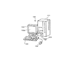
図1は、本発明が適用されるコンピュータの概観斜視図である。コンピュータ100は、本体部101と、表示部102と、キーボード103と、マウス104とを備える。
FIG. 1 is a schematic perspective view of a computer to which the present invention is applied. The
本体部101は、内部にCPU、RAMメモリ、ハードディスク等を内蔵する。本体部101には、フレキシブルディスク(FD)が挿入されるFD挿入口101aと、CD−ROM200が挿入されるCD−ROM挿入口101bと有する。
The
表示部102は、本体部101からの指示により蛍光面(又は液晶面)102aに画面表示を行う。キーボード103は、コンピュータ100内にユーザの指示や文字情報を入力するためのものである。また、マウス104は、蛍光面102a上の任意の位置を指定することでその位置に応じた指示を入力する。
The
本実施例では、CD−ROM200に電磁界シミュレートプログラムが記憶される。CD−ROM200がCD−ROM挿入口101bから挿入され、CD−ROM200に記憶された電磁界シミュレートプログラムが本体部101内のハードディスクにインストールされる。そして、電磁界シミュレートプログラムが起動されると、コンピュータ100は電磁界シミュレータとして機能する。
In this embodiment, an electromagnetic field simulation program is stored in the CD-
図2は、コンピュータ100のハードウェア構成図である。コンピュータ100は、CPU111と、RAM112と、ハードディスクコントローラ113と、FDドライブ114と、CD−ROMドライブ115と、マウスコントローラ116と、キーボードコントローラ117と、ディスプレイコントローラ118とを備え、各々バス110を介して接続される。
FIG. 2 is a hardware configuration diagram of the
CPU111は、本実施例の電磁界シミュレートプログラムや、その他の種々のプログラムを実行する。
The
RAM112は、CPU111のワーキングメモリであり、ハードディスク220にインストールされた電磁界シミュレートプログラムが一旦ロードされる。CPU111は、RAM112から電磁界シミュレートプログラムを読み出して、当該プログラムを実行することができる。
A
ハードディスクコントローラ113は、ハードディスク220へのアクセスを制御するためのものである。FDドライブ114はFD挿入口101aから挿入されたFD210へのアクセスを、CD−ROMドライブ115はCD−ROM挿入口101bより挿入されたCD−ROM200へのアクセス制御する。
The
また、マウスコントローラ116はマウス104を制御し、キーボードコントローラ117はキーボード103を制御し、ディスプレイコントローラ118は表示部102を制御する。
The
ハードディスクコントローラ113等は、CPU111からの制御信号に基づいて、ハードディスク220等を制御することになる。
The
図3は、本実施例における電磁界シミュレートプログラムの一実施形態を示す図である。 FIG. 3 is a diagram showing an embodiment of the electromagnetic field simulation program in the present embodiment.
電磁界シミュレートプログラム300は、コンピュータ100を、電磁界シミュレートとして動作させるものである。図3に示すように、本プログラム300は、シミュレート演算部310と、電磁界解析部320と、表示部330とを有する。この電磁界シミュレートプログラム300の各要素の詳細は後述する。
The electromagnetic
図4は、電磁界シミュレータの機能ブロック図の一例を示す図である。電磁界シミュレータ400は、図3に示す電磁界シミュレートプログラム300がコンピュータ100にインストールされて実行されることにより構成されるものである。
FIG. 4 is a diagram illustrating an example of a functional block diagram of the electromagnetic field simulator. The
電磁界シミュレータ400の各ブロック部は、図3の電磁界シミュレートプログラム300の各要素に対応するが、CPU111等のハードウェアと、コンピュータ100で実行されるOSやアプリケーションプログラムとの組合わせで構成される。図3の電磁界シミュレートプログラム300の各要素は、それらのうちアプリケーションプログラムのみにより構成される。
Each block unit of the
図4に示すように、電磁界シミュレータ400は、シミュレート演算部410と、電磁界解析部420と、表示部430と、記憶部440とを有する。
As illustrated in FIG. 4, the
シミュレート演算部410は、更に、解析モデル設定部411と、波源設定部412と、計算条件設定部413と、波長演算部414と、係数算出部415と、FDTD演算部416とを有する。
The
解析モデル設定部411、波源設定部412、及び計算条件設定部413は、ユーザにより夫々入力された、解析モデル、波源、計算条件の各データから、解析モデル、波源、計算条件が各々設定される。例えば、これらのデータは記憶部440に記憶されることで設定される。
The analysis
波長演算部414は、解析モデル設定部411により設定された解析モデルと、波源設定部412により設定された波源と、から物質内部(例えば、金属物質)の波長を演算する。
The
係数算出部415は、波長演算部414により演算された物質内部の波長と、計算条件設定部413により設定された計算条件とから種々の係数を算出する。
The
係数算出部415は、分極電流の第1の計算式における係数を算出する分極電流用の第1の係数算出部4151と、分極電流の第2の計算式における係数を算出する分極電流用の第2の係数算出部4152と、電界と磁界の計算式の係数を算出する電磁界係数算出部4153とを有する。
The
分極電流用の各係数は、波長演算部414により演算された波長に基づいて、第1の係数算出部4151又は第2の係数算出部4152のいずれか一方において演算される。そして、その係数に基づいて、電磁界係数算出部4153において、FDTD法による電磁界の計算式における係数が算出される。
Each coefficient for the polarization current is calculated in either the first
FDTD演算部416は、係数算出部415により算出された各係数から、実際にFDTD法における各種演算式を演算する。
The
電磁界解析部420は、FDTD演算部416で演算された値を記憶部440に記憶する。例えば、FDTD演算部416で時間ステップ毎に電界が演算され、電磁界解析部420においてその値を2乗し、各々記憶部440に積算した値を記憶することで、電界の平均強度を得ることができる。
The electromagnetic
表示部430(図1の表示部102に対応)は、電磁界解析部420からの解析結果を表示する。例えば、表示部430は、光の強度分布が視覚的にわかるように表示する。
The display unit 430 (corresponding to the
次にFDTD法について説明する。電磁界におけるマクスウェル方程式は、以下の2式で示される。 Next, the FDTD method will be described. The Maxwell equation in an electromagnetic field is expressed by the following two equations.
ここで、Eは電界ベクトル、Hは磁界ベクトル、εは誘電率、σは導電率、μは透磁率を夫々示す。式(2)及び式(3)より得られる電磁界成分の時間変化をFDTD法で算出する式を以下に示す。(Allen Taflove, Susan C. Hagness : "Computational Electrodynamics" (ARTECH HOUCE, INC.)より) Here, E represents an electric field vector, H represents a magnetic field vector, ε represents a dielectric constant, σ represents a conductivity, and μ represents a magnetic permeability. An expression for calculating the time change of the electromagnetic field component obtained from Expression (2) and Expression (3) by the FDTD method is shown below. (From Allen Taflove, Susan C. Hagness: "Computational Electrodynamics" (ARTECH HOUCE, INC.))
ここで、Ex、Ey、Ezは電界の各成分、Hx、Hy、Hzは磁界の各成分、σ*は磁気伝導率、Δx、Δy、Δzは空間グリッド幅、Δtは時間分割幅を夫々示す。電磁界成分の右下に付された添字i、j、kは空間グリッドの番号であり、シミュレート空間上の座標を示す。また、電磁界成分に付された添字n、n+1は時間ステップを示す番号である。時間ステップが一つ進むと、時間がΔtだけ進むことになる。 Here, Ex, Ey, Ez are each component of the electric field, Hx, Hy, Hz are each component of the magnetic field, σ * is the magnetic conductivity, Δx, Δy, Δz are the spatial grid width, and Δt is the time division width, respectively. . The subscripts i, j, and k attached to the lower right of the electromagnetic field component are space grid numbers and indicate coordinates in the simulated space. The subscripts n and n + 1 attached to the electromagnetic field component are numbers indicating time steps. When one time step is advanced, the time is advanced by Δt.
図5は、FDTD法が適用される解析モデルを分割した一つのセル500を示す。そして、セル500における電界、磁界の各成分の空間配置を示している。シミュレート空間には、このようなセル500が複数存在する。
FIG. 5 shows one
FDTD法では、各セル500の辺の中点520に、辺に平行な電界成分が配置され、セル500の各面の中点530に、面に垂直な磁界成分が配置される。
In the FDTD method, an electric field component parallel to the side is arranged at the
図5に示す例では、頂点510の位置座標を(i、j、k)とすると、辺の中点520である、(i+1/2、j、k)、(i、j+1/2、k)、(i、j、k+1/2)に電界の各成分Ex、Ey、Ezが夫々配置される。
In the example shown in FIG. 5, if the position coordinates of the
また、磁界の各成分Hx、Hy、Hzは、夫々面の中点530である、(i、j+1/2、k+1/2)、(i+1/2、j、k+1/2)、(i+1/2、j+1/2、k)に配置される。「1/2」のグリッド上に電界、磁界の各成分が配置されることがFDTD法の特徴でもある。
Further, the magnetic field components Hx, Hy, and Hz are (i, j + 1/2, k + 1/2), (i + 1/2, j, k + 1/2), (i + 1/2), which are the
本電磁界シミュレータ400は、ある時刻(n−1)における電磁界の空間分布を用いて、次の時刻(n)における電磁界の空間分布を算出することを繰り返すことで対象モデルの解析を行うようにしている。
The
尚、前述の式(4)と式(5)は、電界、磁界のX成分のみの計算式を示しているが、電界、磁界のY成分、Z成分の計算式もこれらの式に対応するように示すことができる。 Note that the above formulas (4) and (5) show calculation formulas for only the X component of the electric field and magnetic field, but the calculation formulas for the Y component and Z component of the electric field and magnetic field also correspond to these formulas. Can be shown as:
FDTD法は、一般に電波解析に用いられるものの、上述したように、金属を含んだ光学解析に適用することも可能である。しかし、この場合、金属物質の材料定数が原因で、式(4)と式(5)から算出される電界磁界の各成分値が発散する問題が生ずる。 Although the FDTD method is generally used for radio wave analysis, as described above, it can also be applied to optical analysis including metal. However, in this case, due to the material constant of the metal substance, there arises a problem that each component value of the electric field calculated from the equations (4) and (5) diverges.
誘電率や導電率などの材料定数は、電磁波の周波数によって変化するが、金属の誘電率は光の周波数において負の値を有する場合が多い。真空の誘電率をε0とすると、波長400nmの光に対して、金、銀、アルミニウムの誘電率は、夫々「−1.08ε0」、「−3.77ε0」、「−23.4ε0」となる。 Material constants such as dielectric constant and electrical conductivity vary with the frequency of electromagnetic waves, but the dielectric constant of metal often has a negative value at the frequency of light. Assuming that the dielectric constant of vacuum is ε 0 , the dielectric constants of gold, silver, and aluminum are “−1.08ε 0 ”, “−3.77ε 0 ”, and “−23.4ε” for light with a wavelength of 400 nm, respectively. 0 ".
具体的には、誘電率εが負のとき、式(4)の右辺第1項の係数内(かっこ内)における分子の部分が正となる。右辺第1項は、同位置座標にける電界成分Exの前の時間ステップ(n−1)を参照する頁(Ex|n−1)であり、係数が正の大きな値をとると、計算ステップが進むに従い、値が指数関数的に増大する。したがって、計算を繰り返すと電界・磁界の各成分値は発散する。 Specifically, when the dielectric constant ε is negative, the numerator portion in the coefficient (in parentheses) of the first term on the right side of Equation (4) is positive. The first term on the right side is a page (Ex | n-1 ) that refers to the time step (n-1) before the electric field component Ex at the same position coordinate, and when the coefficient takes a large positive value, the calculation step As the value proceeds, the value increases exponentially. Therefore, when the calculation is repeated, each component value of the electric field / magnetic field diverges.
このような発散の問題に対して、前述の非特許文献3に示されるように、分極電流を用いたFDTD法による計算式がある。以下詳細に説明する。
To solve such a problem of divergence, there is a calculation formula based on the FDTD method using a polarization current as shown in
一般に、複素誘電率ε*は、物質の誘電率εrと導電率σの双方を含んだ材料定数であり、次式で示すことができる。 In general, the complex dielectric constant ε * is a material constant including both the dielectric constant εr and the electrical conductivity σ of a substance, and can be expressed by the following equation.
ここで、ωは光の角周波数である。 Here, ω is the angular frequency of light.
電界Eに複素誘電率ε*を掛けると電束密度Dが得られる。この電束密度Dを用いると、上述の式(2)は、次のようにも表記できる。 When the electric field E is multiplied by the complex dielectric constant ε * , the electric flux density D is obtained. When this electric flux density D is used, the above equation (2) can also be expressed as follows.
物質が負の誘電率を有するとは、式(6)のεrが負であることを意味する。分極を導入した場合に、電束密度Dと分極とは次の関係にある。 The substance having a negative dielectric constant means that ε r in the formula (6) is negative. When polarization is introduced, the electric flux density D and the polarization are in the following relationship.
ε∞は、分極が発生しない高い周波数の電磁波における物質の誘電率であり、瞬間誘電率と呼ばれる。Pは分極である。分極Pは、電界Eとともに時間変化し、その変化は物質の分極特性により決まる。例えば、ドルーデ型の分散特性を仮定すると、分極Pは次の微分方程式に従う。 epsilon ∞ is the dielectric constant of the material in the electromagnetic high-frequency polarization does not occur is referred to as the instantaneous dielectric constant. P is polarization. The polarization P changes with time with the electric field E, and the change is determined by the polarization characteristics of the substance. For example, assuming a Drude type dispersion characteristic, the polarization P follows the following differential equation.
ここで、Γとωpは分散特性を決める定数である。 Here, Γ and ω p are constants that determine the dispersion characteristics.
または、 Or
で定義される分極電流を用いると、分極電流Jは次の微分方程式に従う。 Is used, the polarization current J obeys the following differential equation.
式(9)と式(11)における物質の誘電率εr、導電率σ、定数Γ及びωpは、次式の関係がある。 The dielectric constant ε r , conductivity σ, constants Γ and ωp of the substances in the equations (9) and (11) have the following relationship.
2つの材料定数εr(誘電率)とσ(導電率)に対して、3つの変数Γ、ωp、ε∞があるため、変数の設定には自由度がある。そこで、瞬間誘電率ε∞を正の値に設定し、式(12)で物質の誘電率εrが負の値になるように、定数Γ及びωpを設定することで、FDTD法による負の誘電率εを有する物質の計算が可能となる。 Since there are three variables Γ, ωp, and ε ∞ for the two material constants ε r (dielectric constant) and σ (conductivity), there is a degree of freedom in setting the variables. Therefore, by setting the instantaneous dielectric constant ε ∞ to a positive value and setting the constants Γ and ωp so that the dielectric constant ε r of the substance becomes a negative value in Equation (12), It is possible to calculate a substance having a dielectric constant ε.
式(8)を式(7)に適用すると、 Applying equation (8) to equation (7),
となる。この式(14)から、式(4)に対応する式を求めると、次式が得られる。 It becomes. When an expression corresponding to the expression (4) is obtained from the expression (14), the following expression is obtained.
この式(15)では、前の時間ステップ(n−1)を参照する右辺第1項(Ex|n−1)の係数が「1」であるため、上述した発散の問題を回避することができる。 In this equation (15), since the coefficient of the first term (Ex | n-1 ) on the right side referring to the previous time step (n-1) is "1", the above-described divergence problem can be avoided. it can.
分極電流Jについては、式(11)より、次式を得る。 For the polarization current J, the following equation is obtained from the equation (11).
式(16)において、分極電流JPの時間ステップは「n+1/2」、「n−1/2」など半整数の値を取る。尚、磁界Hの計算は通常のFDTD法と同様に式(5)を用いる。 In the formula (16), the time step of the polarization current J P is "n + 1/2" takes the value of the half integer, such as "n-1/2". Incidentally, the calculation of the magnetic field H uses the formula (5) as in the normal FDTD method.
FDTD法を用いて金属を含むモデルの光学解析の一般的な手法は、磁界Hは式(5)を用い、電界Eは式(15)を用い、分極電流Jは式(16)を用いて計算を行う。 As a general method of optical analysis of a model including a metal using the FDTD method, the magnetic field H uses the equation (5), the electric field E uses the equation (15), and the polarization current J uses the equation (16). Perform the calculation.
次に、このような式を用いて解析を行う場合の問題点について考察する。 Next, the problem in the case of performing analysis using such an expression will be considered.
図6は、解析モデルの例を示す。FDTD法を用いた光学解析の例として、薄膜550の透過率を、上述した分極電流JPを用いたFDTD法で計算する。 FIG. 6 shows an example of an analysis model. Examples of optical analysis using the FDTD method, the transmittance of the thin film 550, calculated by the FDTD method using a polarization current J P described above.
薄膜550の厚さは「80nm」であり、屈折率を「1」、光の波長を「780nm」とし、薄膜550に垂直に光を入射させ、その入射光と透過光との強度の比をとり、薄膜550の透過率(|Et|2/|Ei|2)を計算した。但し、消衰係数(光が物質内を透過するときにどれだけ光を吸収するかの度合い)を「1.5」から「5」まで変化させ、透過率を変化させる。また、解析空間を分割するグリッド間隔を「20nm」と「5nm」の2種類の条件で計算する。 The thickness of the thin film 550 is “80 nm”, the refractive index is “1”, the wavelength of light is “780 nm”, light is incident perpendicularly to the thin film 550, and the ratio of the intensity of the incident light to the transmitted light is determined. Then, the transmittance (| Et | 2 / | Ei | 2 ) of the thin film 550 was calculated. However, the extinction coefficient (how much light is absorbed when light passes through the substance) is changed from “1.5” to “5” to change the transmittance. Further, the grid interval for dividing the analysis space is calculated under two kinds of conditions of “20 nm” and “5 nm”.
上述の式(15)と式(16)内には、屈折率nと消衰係数κは示されていない。一般に、屈折率nと消衰係数κとは、 In the above equations (15) and (16), the refractive index n and the extinction coefficient κ are not shown. In general, the refractive index n and the extinction coefficient κ are
の関係があるため、これを用いて式(15)、式(16)を計算する。 Therefore, equations (15) and (16) are calculated using this relationship.
図7(A)は、この解析結果を示すグラフである。横軸は消衰係数κ、縦軸はFDTD法による透過率と厳密な演算による透過率との相対誤差(FDTD法の計算誤差)を示す。薄膜550の透過率は屈折率nと、消衰係数κと、厚さとから正確に演算できるため、この演算により得た値が厳密な演算による透過率となる。 FIG. 7A is a graph showing the analysis results. The horizontal axis represents the extinction coefficient κ, and the vertical axis represents the relative error (calculation error of the FDTD method) between the transmittance by the FDTD method and the transmittance by a strict calculation. Since the transmittance of the thin film 550 can be accurately calculated from the refractive index n, the extinction coefficient κ, and the thickness, the value obtained by this calculation becomes the transmittance by a strict calculation.
一般に、消衰係数が大きいほど光強度が減衰するため、相対誤差は大きくなるものの、図7(A)に示すように、グリッド間隔が「5nm」のとき、消衰係数を大きくしても、相対誤差は小さく抑えることができた(消衰係数「5」のとき誤差は約「2%」)。 In general, as the extinction coefficient increases, the light intensity decreases, so the relative error increases. However, when the grid interval is “5 nm” as shown in FIG. The relative error could be kept small (the error was about “2%” when the extinction coefficient was “5”).
しかし、グリッド間隔が「20nm」としたとき消衰係数が大きいと、誤差は大きく増大する。図7(A)の例では、消衰係数が「5」のとき誤差は約「30%」となった。 However, if the extinction coefficient is large when the grid interval is “20 nm”, the error greatly increases. In the example of FIG. 7A, when the extinction coefficient is “5”, the error is about “30%”.
図7(A)に示すような誤差を抑えるためには、グリッド間隔を小さくすればよいことは明らかである。しかし、例えば、グリッド間隔を「1/2」にすると、3次元解析ではグリッド数は「8」倍になる。 In order to suppress the error as shown in FIG. 7A, it is obvious that the grid interval should be reduced. However, for example, when the grid interval is set to “½”, the number of grids is “8” times in the three-dimensional analysis.
一方、時間ステップΔtについては、FDTD法の計算が発散せずに安定に計算を行うために、一般に、以下の条件を満たす必要がある。 On the other hand, the time step Δt generally needs to satisfy the following conditions in order to perform stable calculation without causing the FDTD method to diverge.
ここで、vは電磁波の速度を示す。 Here, v indicates the speed of the electromagnetic wave.
これにより、式(19)からグリッド間隔を「1/2」にすると、時間ステップΔtも「1/2」小さくする必要がある。これでは、計算時間も多くなり、使用される値が増加することでメモリ容量を増大しなければならない。従って、計算コストを増加させる。 Accordingly, when the grid interval is set to “½” from the equation (19), the time step Δt also needs to be reduced by “½”. This increases the calculation time, and the memory capacity must be increased by increasing the values used. Therefore, the calculation cost is increased.
次に、グリッド間隔が粗い場合でも、計算誤差を小さく抑えるとともに計算コストも低くするようにした計算手法について述べる。 Next, a calculation method is described in which calculation errors are reduced and calculation costs are reduced even when the grid interval is rough.
物質内部の分極電流Pを示す式(11)において、時間微分を差分に置き換えると、 In the equation (11) showing the polarization current P inside the substance, if the time derivative is replaced with a difference,
となる。 It becomes.
式(20)に着目すると、左辺第1項の分極電流JPの時間ステップは、「n+1/2」、「n−1/2」で半整数となっている。一方、左辺第2項の分極電流JPの時間ステップは「n」と整数となっている。一方、電界Eは時間ステップが整数値をとる。 Focusing on Expression (20), the time step of the polarization current J P of the left-hand first term is "n + 1/2", half-integer "n-1/2". On the other hand, the time step of the polarization current J P on the left side second term is an integral "n". On the other hand, the time step of the electric field E takes an integer value.
そこで、時間的に前後する、分極電流JPの2つの半整数ステップの値(「n+1/2」と「n−1/2」)から次式により整数ステップの値「n」を求めるようにする。 Therefore, chronologically successive, two half-integer steps the value of polarization current J P ( "n + 1/2" and "n-1/2") to determine a value "n" an integer steps by the following formula To do.
但し、パラメータfは、(0≦f≦1)を満たす。 However, the parameter f satisfies (0 ≦ f ≦ 1).
式(21)に示すように、整数ステップの分極電流の値(J|n)には、パラメータfの範囲で任意性がある。通常の計算では、平均であるf=1/2で式(21)を計算する。図7(B)はその概念図である。そのときの漸化式が上述の式(16)である。 As shown in the equation (21), the value (J | n ) of the polarization current in the integer step has an arbitrary property within the range of the parameter f. In a normal calculation, equation (21) is calculated with an average f = 1/2. FIG. 7B is a conceptual diagram thereof. The recurrence formula at that time is the above-described formula (16).
一方、分極電流(J|n)の置き換えとして、f=1/2ではなく、f=1の場合を考える。すなわち、整数ステップの値として、半整数ステップ進んだ値を用いて計算する。この場合、分極電流JPの式(16)に対応する式は次のように示すことができる。 On the other hand, as a replacement of the polarization current (J | n ), consider the case where f = 1 instead of f = 1/2. That is, calculation is performed using a value advanced by a half integer step as the value of the integer step. In this case, the expression corresponding to equation (16) polarization current J P can be represented as follows.
分極電流Jpの式を式(16)から式(22)に変更することで、誤差の発生する傾向が変化し、グリッド間隔が大きい条件でも誤差の発生を低減することができる。次に、この点について考察する。 By changing the expression of the polarization current Jp from the expression (16) to the expression (22), the tendency of the error to change is changed, and the occurrence of the error can be reduced even under a condition where the grid interval is large. Next, this point will be considered.
図8は、上述の図6に示すモデルにおいて、グリッド間隔を「20nm」とし、式(16)により計算した場合(通常の計算式)と、式(22)を用いて計算した場合(本発明の計算式)との比較結果である。 FIG. 8 shows a case where the grid interval is set to “20 nm” in the model shown in FIG. 6 and the calculation is performed according to the equation (16) (ordinary calculation equation) and the calculation according to the equation (22) (the present invention). It is a comparison result with the calculation formula.
図8に示すように、消衰係数が小さいときには、通常の計算式による式(16)を用いた方が誤差は小さい。消衰係数が約「3.4」になると、式(22)を用いた場合は誤差が最小となる。そして、消衰係数がそれより大きくなると、式(22)を用いた方が、通常の計算式である式(16)を用いた場合よりも、誤差は小さくなる。 As shown in FIG. 8, when the extinction coefficient is small, the error is smaller when the equation (16) based on the normal calculation formula is used. When the extinction coefficient is about “3.4”, the error is minimized when Expression (22) is used. When the extinction coefficient is larger than that, the error is smaller when the equation (22) is used than when the equation (16) that is a normal calculation equation is used.
つまり、式(22)を用いるとグリッド間隔を「20nm」と大きくとっても誤差を低減することができる。但し、グリッド間隔が十分小さい場合は、式(16)を用いても誤差は十分小さくすることができる(図7(A)参照)。 In other words, using equation (22), the error can be reduced even if the grid interval is set to be as large as “20 nm”. However, when the grid interval is sufficiently small, the error can be sufficiently reduced even if Expression (16) is used (see FIG. 7A).
従って、グリッド間隔を何らかの手法により評価し、式(16)を用いる場合と式(22)を用いる場合とでどちらが適切かを判断し、誤差の小さい方を適用するようにすれば、計算コストの増加等の問題は回避することができる。 Therefore, if the grid interval is evaluated by some method, it is determined which is appropriate when using the equation (16) and when using the equation (22), and the method with the smaller error is applied. Problems such as an increase can be avoided.
本実施例では、このグリッド間隔の評価、即ち、式(16)を用いればよいいか、式(22)を用いればよいかの判断は、金属物質に入射する光の波長λ’により行う。 In this embodiment, the evaluation of the grid interval, that is, whether to use the equation (16) or the equation (22) is performed based on the wavelength λ ′ of the light incident on the metal material.
物質内部の光の波長λ’は、 The wavelength λ ′ of the light inside the substance is
により得ることができる。この式(23)において、複素誘電率ε*は、屈折率nと消衰係数κから次式で算出される。 Can be obtained. In this equation (23), the complex dielectric constant ε * is calculated from the refractive index n and the extinction coefficient κ by the following equation.
図9は、図8のデータに対して、物質内部の波長λ’をグリッド間隔Δxで割った値を横軸にとり、縦軸を相対誤差としたときのグラフである。グラフの左側ほど物質内部の波長に対するグリッド間隔は大きくなる。 FIG. 9 is a graph when the horizontal axis represents the value obtained by dividing the wavelength λ ′ inside the substance by the grid interval Δx and the vertical axis represents the relative error with respect to the data of FIG. 8. The grid interval with respect to the wavelength inside the substance increases toward the left side of the graph.
横軸λ’/Δxの「10」に着目すると、分極演算を示す式(16)の計算式(通常の計算式)を用いた場合の誤差は約「−15.7%」であった。一方、同様に分極演算を示す式(22)の計算式(本発明の計算式)を用いた場合の誤差は約「−7.5%」となった。つまり、横軸「10」の値では、式(22)の方が誤差は低減できる。 Paying attention to “10” on the horizontal axis λ ′ / Δx, the error when using the calculation formula (ordinary calculation formula) of the formula (16) indicating the polarization calculation was about “−15.7%”. On the other hand, the error in the case of using the calculation formula (22) that similarly shows the polarization operation (the calculation formula of the present invention) was about “−7.5%”. That is, in the value of “10” on the horizontal axis, the error can be reduced by the equation (22).
また、横軸「10」より小さい領域でも、式(22)の方が式(16)を用いた場合よりも誤差を低減することができる。 Even in a region smaller than the horizontal axis “10”, the error can be reduced in the expression (22) than in the case where the expression (16) is used.
すなわち、図9から、グリッド間隔Δxが物質内部の波長λ’の「1/10」以上のとき(「λ’/Δx=10」より小さい領域)は、式(22)を用いた方が式(16)を用いるよりも誤差を低減できる。 That is, from FIG. 9, when the grid interval Δx is equal to or greater than “1/10” of the wavelength λ ′ inside the substance (region smaller than “λ ′ / Δx = 10”), the equation (22) is more The error can be reduced as compared with (16).
一方、グリッド間隔Δxが物質内部の波長λ’の「1/10」より小さいとき(「λ’/Δx=10」よりも大きい領域)は、通常の計算式である式(16)を用いた方が誤差を低減できる。 On the other hand, when the grid interval Δx is smaller than “1/10” of the wavelength λ ′ inside the substance (a region larger than “λ ′ / Δx = 10”), Formula (16) which is a normal calculation formula is used. This can reduce the error.
分極電流JPの計算式(式(16)と式(22))を切り替える基準としては、グリッド間隔が波長の「1/10」とすることで、グリッド間隔が大きい場合でも、演算結果による誤差を低減することができるのである。 The reference for switching formula for polarization current J P (Equation (16) Equation (22)), and that the grid spacing is set to "1/10" of the wavelength, even if the grid spacing is large, the error due to the operation result Can be reduced.
グリッド間隔が同じであれば、図7(A)に示すように、消衰係数が大きいほど誤差が大きくなる。負の誘電率を有する金属は大きな消衰係数を持つ。一部にでも材料として金属が含まれるモデルの光学解析のためにFDTD法で計算する場合は、金属のような消衰係数の大きな物質の分極を計算しなくてはならない。従って、上述した計算式の切り替えは光学解析で特に有用である。 If the grid interval is the same, the error increases as the extinction coefficient increases, as shown in FIG. A metal having a negative dielectric constant has a large extinction coefficient. In the case of calculating by the FDTD method for optical analysis of a model including a metal as a material in part, the polarization of a substance having a large extinction coefficient such as a metal must be calculated. Therefore, the above-described calculation formula switching is particularly useful in optical analysis.
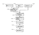
図10は、以上のようなFDTD法による計算を行う場合の処理の動作を示すフローチャートを示す図である。図4に示す電磁界シミュレータ400において実行される処理である。
FIG. 10 is a diagram showing a flowchart showing the processing operation in the case of performing the calculation by the FDTD method as described above. This is a process executed in the
まず、解析モデル設定部411に解析モデルの各値が入力される(S501)。具体的には、物体の形状と、透過率εと、透磁率μ、導電率σ等の各値が入力される。これにより、解析対象の解析モデルが設定される。 First, each value of the analysis model is input to the analysis model setting unit 411 (S501). Specifically, values such as the shape of the object, the transmittance ε, the permeability μ, the conductivity σ, and the like are input. Thereby, an analysis model to be analyzed is set.
また、波源設定部412に波源を定義する各値が入力される(S502)。具体的には、波源の位置と形状、電界振幅E0、光の角周波数ω、光の初期位相φ等の各値が入力される。これにより、解析モデルにおける波源が設定される。また、波源設定部412により、電磁界の空間分布(式(4)や式(5)、更に、式(16)や式(22)など)を計算するために電磁波を発生させるの波源位置と強度とが設定される。これらを示す値が各々入力される。
Each value defining the wave source is input to the wave source setting unit 412 (S502). Specifically, values such as the position and shape of the wave source, the electric field amplitude E 0 , the angular frequency ω of light, and the initial phase φ of light are input. Thereby, the wave source in the analysis model is set. In addition, the wave
更に、計算条件設定部413に計算条件の各値が入力される(S503)。具体的には、空間的なグリッド幅Δx、Δy、Δzと、時間分割幅Δtの各値が入力される。解析モデルにおける空間的なきざみ量(粗さ)と時間的なきざみ量(粗さ)が入力される。このΔx等により、電磁界シミュレーションにおける時空間的な粗さが設定されるため、計算条件設定部413はグリッド設定部の機能を含む。
Further, each value of the calculation condition is input to the calculation condition setting unit 413 (S503). Specifically, the values of the spatial grid widths Δx, Δy, Δz and the time division width Δt are input. A spatial step size (roughness) and a temporal step size (roughness) in the analysis model are input. Since the spatio-temporal roughness in the electromagnetic field simulation is set by this Δx and the like, the calculation
次いで、波長演算部414において、入力された解析モデルと波源とから、物質内部における波長λ’を計算する(S504)。具体的には、式(23)を演算する。
Next, the
次いで、係数算出部415において、物質内部の波長λ’と、設定された計算条件とから分極電流の計算式の係数を算出する(S505)。
Next, the
このS504とS505の処理の詳細を図11に示す。S504が図11のS601とS602に対応し、S505がS603乃至S605に対応する。 Details of the processing of S504 and S505 are shown in FIG. S504 corresponds to S601 and S602 in FIG. 11, and S505 corresponds to S603 to S605.
まず、波長演算部414において複素誘電率ε*を計算する(S601)。式(24)により演算する。そして、複素誘電率ε*から式(23)を用いて波長λ’を演算する(S602)。 First, the complex dielectric constant ε * is calculated in the wavelength calculation unit 414 (S601). Calculation is performed according to equation (24). Then, the wavelength λ ′ is calculated from the complex dielectric constant ε * using the equation (23) (S602).
次いで、係数算出部415において、セルサイズの評価を行う(S603)。即ち、上述した、グリッド間隔が波長λ’の「1/10」以上否かを判断する。グリッド間隔は計算条件設定部413に入力され、波長λ’はS602(S504)で計算されるため、これらを比較することで判断可能である。
Next, the
グリッド間隔が波長λ’の「1/10」以上のとき(S603でYES)、分極電流用の第1の係数算出部4151において、分極演算の式(22)での係数値を算出する(S604)。一方、グリッド間隔が波長λ’の「1/10」より小さいとき(S603でNO)、分極電流用の第2の係数算出部4152において、分極演算の式(16)での係数値を算出する。
When the grid interval is equal to or greater than “1/10” of the wavelength λ ′ (YES in S603), the first
分極電流の式(16)と式(22)とを一般化すると、 Generalizing the equations (16) and (22) of the polarization current,
となる。式(16)と式(22)の違いは係数だけである。S603の条件に従い、まず係数を算出し、その後、後段のFDTD法による式(16)又は式(22)を計算する。 It becomes. The difference between Equation (16) and Equation (22) is only the coefficient. In accordance with the condition of S603, first, a coefficient is calculated, and then equation (16) or equation (22) is calculated by the subsequent FDTD method.
式(25)と式(22)とから、係数は From Equation (25) and Equation (22), the coefficient is
となる。 It becomes.
即ち、グリッド間隔が波長λ’の「1/10」以上のとき(S603でYES)、グリッド間隔が大きいとして、式(26)と式(27)を用いて係数を求める(S604)。 That is, when the grid interval is equal to or greater than “1/10” of the wavelength λ ′ (YES in S603), the coefficient is obtained using Equation (26) and Equation (27) assuming that the grid interval is large (S604).
一方、式(25)と式(16)とから、係数は、 On the other hand, from Equation (25) and Equation (16), the coefficient is
となる。 It becomes.
即ち、グリッド間隔が波長λ’の「1/10」より小さいとき(S603でNO)、グリッド間隔が小さいとして、式(28)と式(29)を用いて係数を求める(S605)。 That is, when the grid interval is smaller than “1/10” of the wavelength λ ′ (NO in S603), it is determined that the grid interval is small, and the coefficient is obtained using Equation (28) and Equation (29) (S605).
尚、分散特性を決める定数Γ、ωpは、屈折率nと消衰係数κと、瞬間誘電率ε∞、及び光の各周波数ωから次式で求めることができる。 The constants Γ and ω p that determine the dispersion characteristics can be obtained from the refractive index n, the extinction coefficient κ, the instantaneous dielectric constant ε ∞ , and each frequency ω of light by the following equation.
また、算出した各係数A、Bは、アクセス速度の速い記憶部440(図2でのRAM112)に記憶される。
The calculated coefficients A and B are stored in the storage unit 440 (
図10に戻り、係数算出部415で各係数を求めると(S505、506)、次いで、FDTD演算部416において、FDTD法による計算が実行される(S507)。上述したように、グリッド間隔が大きいときは、式(22)を用いて分極演算を行う。グリッド間隔が小さいときは、式(16)を用いて分極演算を行う。
Returning to FIG. 10, when the
次いで、電磁界解析部420で、計算結果を解析する(S508)。具体的には、各々演算した電磁界の各値E、Hを2乗した値を記憶部440に記憶し、積算した値を記憶部440に保持する。
Next, the electromagnetic
次いで、電磁界解析部420から解析結果が出力される(S509)。例えば、表示部430に出力され解析結果が表示される。或いは、ハードディスク220に解析結果が記憶される。
Next, an analysis result is output from the electromagnetic field analysis unit 420 (S509). For example, the analysis result is displayed on the
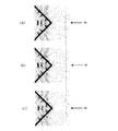
図12の各図は、表示部430に表示される解析結果の例である。即ち、頂角90°のプローブに、厚さ「70.7nm」の金の薄膜を設定したモデルについて、簡易的に2次元空間で計算した結果である。光の波長は「400nm」とし、光は各図の左側から右側に伝播する。
Each diagram in FIG. 12 is an example of an analysis result displayed on the
図12(A)は、グリッド間隔を「5nm」とし、通常の演算式である、式(16)により演算した結果を示す。また、同図(B)は、グリッド間隔を「20nm」で本実施例による式(22)により演算した結果、同図(C)はグリッド間隔を同じく「20nm」で通常の演算式である式(16)により演算した結果を夫々示す。 FIG. 12A shows the result of calculation according to Expression (16), which is a normal calculation expression, with the grid interval set to “5 nm”. FIG. 5B shows the result of calculation according to the equation (22) according to the present embodiment when the grid interval is “20 nm”, and FIG. 5C is an equation that is a normal calculation equation when the grid interval is also “20 nm”. The result calculated by (16) is shown, respectively.
この場合に、金の薄膜内部の波長λ’は式(23)より、「156.0nm」となった。「20nm」のグリッド間隔は波長λ’の「1/10」より大きく、図11に示す適用条件を満たしている。 In this case, the wavelength λ ′ inside the gold thin film was “156.0 nm” from the equation (23). The grid interval of “20 nm” is larger than “1/10” of the wavelength λ ′ and satisfies the application condition shown in FIG.
矢印Mで示す領域に着目すると、式(22)を用いた演算結果(同図(B))と式16を用いた演算結果(同図(C))とでは、式(22)を用いた方が、グリッド間隔を小さくした演算結果(同図(A))に近いことが理解される。 Focusing on the area indicated by the arrow M, the calculation result using the equation (22) (FIG. (B)) and the calculation result using the equation (16) (FIG. (C)) used the equation (22). It is understood that this is closer to the calculation result ((A) in the figure) in which the grid interval is reduced.
即ち、グリッド間隔が大きい場合には、式(22)による演算を行った方がより誤差が小さく、概算値として用いることが可能な値を得ることができる。 That is, when the grid interval is large, the error is smaller when the calculation according to the equation (22) is performed, and a value that can be used as an approximate value can be obtained.
以上説明したように、空間グリッド間隔が大きい場合には、式(22)を用いて分極によるFDTD法の演算を行い、空間グリッド間隔が小さい場合には、式(16)を用いて分極によるFDTD法の演算を行うようにしたので、本電磁界シミュレータ400は、計算コストを小さくすることができるとともに、演算による誤差も小さい解析結果を得ることが可能となる。
As described above, when the spatial grid interval is large, the calculation of the FDTD method by polarization is performed using Equation (22), and when the spatial grid interval is small, the FDTD by polarization is calculated using Equation (16). Since the calculation of the modulo is performed, the
尚、このような解析モデルは、金属薄膜の針から光を照射してサンプルの表面を測定するSNOM(Scanning Near-field Optical Microscope)顕微鏡に適用して好適である。本電磁界シミュレータ400はこのようなSNOM顕微鏡における光の振る舞いを解析するのに役立つ。
Such an analysis model is suitable for application to a SNOM (Scanning Near-field Optical Microscope) microscope that measures the surface of a sample by irradiating light from a metal thin film needle. The
上述した例において、分散モデルとしてドルーテ型分散モデルを例にして説明したが、それ以外にも、ローレンツ型等の他の分散モデルでも同様に本電磁界シミュレータ400において解析可能であり、上述した例と同様の作用効果を奏する。
In the above-described example, the drute type dispersion model has been described as an example of the dispersion model, but other dispersion models such as the Lorentz type can be similarly analyzed in the
また、上述した例において、空間グリッド間隔が大きいか否かの基準として、グリッド間隔が金属物質内部の光の波長λ’の「1/10」以上か否かで説明した。勿論、それ以外にも「1/10」近傍の値を基準としても、上述した例と同様に実施可能で同様の作用効果を奏する。 Further, in the above-described example, the description was made based on whether or not the grid interval is “1/10” or more of the wavelength λ ′ of the light inside the metal material, as a reference whether or not the spatial grid interval is large. Of course, in addition to this, even if a value in the vicinity of “1/10” is used as a reference, it can be implemented in the same manner as in the above-described example, and the same effects can be obtained.
更に、上述した例では、CD−ROM200に本実施例における電磁界シミュレートプログラムが記憶されるものとして説明した。勿論、例えば、フレキシブルディスク210などCD−ROM200以外の記録媒体に記録されていてもよい。コンピュータ100でそのプログラムを読み出して実行することができれば、上述の例と同様に実施可能で、同様の作用効果を奏する。
Furthermore, in the above-described example, the CD-
以上まとめると付記のようになる。 The above is summarized as an appendix.
(付記1)
ある時刻(n−1)における電磁界の空間分布を用いて、次の時刻(n)の電磁界の空間分布を算出することを繰り返す電磁界シミュレータにおいて、
電磁界のシミュレーションにおける時間上及び空間上の粗さを設定する計算条件設定部と、
シミュレート空間上の各位置における電磁界の物理係数を設定する係数設定部と、
前記時刻(n−1)における電磁界の空間分布と物質内部の分極電流の空間分布、及び前記係数設定部で設定された前記物理係数とを用いて、前記時刻(n)における電磁界の空間分布と物質内部の分極電流の空間分布とを算出する分極算出部と、を備え、
前記係数設定部は、前記計算条件設定部にて設定された前記空間上の粗さに基づいて、分極算出部において前記分極電流の空間分布を算出するために使用する第1の計算式を第2の計算式に切り替えるようにし、
前記分極算出部は、前記第2の計算式を用いて、前記時刻(n)における前記分極電流の空間分布を算出することを特徴とする電磁界シミュレータ。
(Appendix 1)
In the electromagnetic field simulator that repeats calculating the spatial distribution of the electromagnetic field at the next time (n) using the spatial distribution of the electromagnetic field at a certain time (n−1),
A calculation condition setting unit for setting roughness on time and space in electromagnetic field simulation;
A coefficient setting unit for setting the physical coefficient of the electromagnetic field at each position on the simulated space;
Using the spatial distribution of the electromagnetic field at the time (n-1), the spatial distribution of the polarization current inside the substance, and the physical coefficient set by the coefficient setting unit, the space of the electromagnetic field at the time (n) A polarization calculator that calculates the distribution and the spatial distribution of the polarization current inside the substance,
The coefficient setting unit has a first calculation formula used for calculating the spatial distribution of the polarization current in the polarization calculation unit based on the roughness in the space set by the calculation condition setting unit. Switch to the
The polarization calculation unit calculates a spatial distribution of the polarization current at the time (n) using the second calculation formula.
(付記2)
更に、前記電磁界の空間分布を計算するために電磁波の発生源を設定する波源設定部を備え、
前記分極算出部は、前記係数設定部で設定された前記物理係数と前記波源設定部で設定された前記波源の波長とに基づいて、前記第1の計算式から前記第2の計算式に切り替える、ことを特徴とする付記1記載の電磁界シミュレータ。
(Appendix 2)
And a wave source setting unit for setting an electromagnetic wave generation source to calculate the spatial distribution of the electromagnetic field,
The polarization calculation unit switches from the first calculation formula to the second calculation formula based on the physical coefficient set by the coefficient setting unit and the wavelength of the wave source set by the wave source setting unit. The electromagnetic field simulator according to
(付記3)
前記係数設定部で設定した前記物理係数から導出される複素誘電率をε*とし、前記波源設定部で夫々設定した前記波長をλ、前記空間上の粗さをΔxとし、更に真空の誘電率をε0とすると、前記係数設定部は、
(Appendix 3)
The complex dielectric constant derived from the physical coefficient set by the coefficient setting unit is ε * , the wavelength set by the wave source setting unit is λ, the roughness on the space is Δx, and the dielectric constant of vacuum Ε 0 , the coefficient setting unit
から得られる変数aの大きさに基づいて、前記第1の計算式から前記第2の計算式に切り替えることを特徴とする付記2記載の電磁界シミュレータ。
The electromagnetic field simulator according to
(付記4)
前記第2の計算式は前後する2つの時間ステップの中間の値を求める算出方法を変更した式であることを特徴する付記1乃至3記載の電磁界シミュレータ。
(Appendix 4)
The electromagnetic field simulator according to any one of
(付記5)
前記第2の計算式は前後する前記時間ステップの中間の値を半整数ステップ進んだ値を用いた計算式であることを特徴とする付記4記載の電磁界シミュレータ。
(Appendix 5)
The electromagnetic field simulator according to
(付記6)
更に、前記波源設定部で設定された前記波源に基づいて、前記電磁波が物質を透過するときの前記物質内の前記電磁波の波長を演算する波長演算部を備え、
前記分極算出部は、前記係数設定部で設定された前記空間上の粗さを示すグリッド間隔が、前記波長演算部で演算した前記物質内の波長よりも十分大きいときは、前記第1の計算式から前記第2の計算式に切り替えることを特徴とする付記1又は2記載の電磁界シミュレータ。
(Appendix 6)
Furthermore, based on the wave source set by the wave source setting unit, a wavelength calculation unit that calculates the wavelength of the electromagnetic wave in the substance when the electromagnetic wave passes through the substance,
When the grid interval indicating the roughness in the space set by the coefficient setting unit is sufficiently larger than the wavelength in the substance calculated by the wavelength calculation unit, the polarization calculation unit performs the first calculation. The electromagnetic field simulator according to
(付記7)
前記分極算出部は、前記グリッド間隔が前記物質内部の波長の「1/10」以上のときに、前記第1の計算式から前記第2の計算式に切り替えることを特徴とする付記6記載の電磁界シミュレータ。
(Appendix 7)
The polarization calculation unit switches from the first calculation formula to the second calculation formula when the grid interval is “1/10” or more of the wavelength inside the substance. Electromagnetic simulator.
(付記8)
ある時刻(n−1)における電磁界の空間分布を用いて、次の時刻(n)の電磁界の空間分布を算出することを繰り返す電磁界シミュレートプログラムにおいて、
電磁界のシミュレーションにおける時間上及び空間上の粗さを設定する計算条件設定処理と、
シミュレート空間上の各位置における電磁界の物理係数を設定する係数設定処理と、
前記時刻(n−1)における電磁界の空間分布と物質内部の分極電流の空間分布、及び前記係数設定部で設定された前記物理係数とを用いて、前記時刻(n)における電磁界の空間分布と物質内部の分極電流の空間分布とを算出する分極算出処理と、をコンピュータに実行させ、
前記係数設定処理では、前記計算条件設定処理にて設定された前記空間上の粗さに基づいて、前記分極算出処理にて前記分極電流の空間分布を算出するために使用する第1の計算式を第2の計算式に切り替えるようにし、
前記分極算出処理では、前記第2の計算式を用いて、前記時刻(n)における前記分極電流の空間分布を算出することをコンピュータに実行させることを特徴とする電磁界シミュレートプログラム。
(Appendix 8)
In the electromagnetic field simulation program that repeatedly calculates the spatial distribution of the electromagnetic field at the next time (n) using the spatial distribution of the electromagnetic field at a certain time (n-1),
Calculation condition setting processing for setting the roughness in time and space in the electromagnetic field simulation,
Coefficient setting processing for setting the physical coefficient of the electromagnetic field at each position in the simulated space;
Using the spatial distribution of the electromagnetic field at the time (n-1), the spatial distribution of the polarization current inside the substance, and the physical coefficient set by the coefficient setting unit, the space of the electromagnetic field at the time (n) Causing the computer to execute a polarization calculation process for calculating the distribution and a spatial distribution of the polarization current inside the substance,
In the coefficient setting process, a first calculation formula used for calculating the spatial distribution of the polarization current in the polarization calculation process based on the roughness in the space set in the calculation condition setting process. To switch to the second formula,
In the polarization calculation process, an electromagnetic field simulation program causing a computer to calculate a spatial distribution of the polarization current at the time (n) using the second calculation formula.
100 コンピュータ
111 CPU
112 RAM
113 ハードディスクコントローラ
115 CD−ROMドライブ
200 CD−ROM
220 ハードディスク
300 電磁界シミュレートプログラム
310、410 シミュレート演算部
314、414 波長演算部
315、415 係数算出部
316、416 FDTD演算部
320、420 電磁界解析部
330、430、102 表示部
400 電磁界シミュレータ
500 セル
100
112 RAM
113
220
Claims (6)
電磁界のシミュレーションにおける時間上及び空間上の粗さを設定する計算条件設定部と、
シミュレート空間上の各位置における電磁界の物理係数を設定する係数設定部と、
前記時刻(n)における電界の空間分布と、時刻(n−1/2)における物質内部の分極電流の空間分布、及び前記係数設定部で設定された前記物理係数とを用いて、時刻(n+1/2)における物質内部の分極電流の空間分布とを算出する分極算出部と、を備え、
前記係数設定部は、前記計算条件設定部にて設定された前記空間上の粗さに基づいて、分極算出部において前記分極電流の空間分布を算出するために使用する第1の計算式を第2の計算式に切り替えるようにし、
前記分極算出部は、前記第2の計算式を用いて、前記時刻(n+1/2)における前記分極電流の空間分布を算出することを特徴とする電磁界シミュレータ。 During time by using the magnetic field spatial distribution of the electric field and time (n + 1/2) in the (n), when calculating the spatial distribution of the electric field of the time (n +1), the time field and the time in the (n + 1/2) (n + 1 In the electromagnetic field simulator that repeatedly calculates the spatial distribution of the magnetic field at time (n + 3/2) using the spatial distribution of the electric field of
A calculation condition setting unit for setting roughness on time and space in electromagnetic field simulation;
A coefficient setting unit for setting the physical coefficient of the electromagnetic field at each position on the simulated space;
Using the spatial distribution of the electric field at the time ( n) , the spatial distribution of the polarization current inside the substance at the time (n−1 / 2) , and the physical coefficient set by the coefficient setting unit, the time (n + 1) A polarization calculation unit that calculates the spatial distribution of the polarization current inside the substance in / 2) ,
The coefficient setting unit has a first calculation formula used for calculating the spatial distribution of the polarization current in the polarization calculation unit based on the roughness in the space set by the calculation condition setting unit. Switch to the calculation formula 2
The polarization calculation unit calculates a spatial distribution of the polarization current at the time (n +1/2 ) using the second calculation formula.
前記分極算出部は、前記係数設定部で設定された前記物理係数と前記波源設定部で設定された前記波源の波長とに基づいて、前記第1の計算式から前記第2の計算式に切り替える、ことを特徴とする請求項1記載の電磁界シミュレータ。 And a wave source setting unit for setting an electromagnetic wave generation source for calculating the spatial distribution of the electromagnetic field,
The polarization calculation unit switches from the first calculation formula to the second calculation formula based on the physical coefficient set by the coefficient setting unit and the wavelength of the wave source set by the wave source setting unit. The electromagnetic field simulator according to claim 1.
電磁界のシミュレーションにおける時間上及び空間上の粗さを設定する計算条件設定処理と、
シミュレート空間上の各位置における電磁界の物理係数を設定する係数設定処理と、
前記時刻(n)における電界の空間分布と、時刻(n−1/2)における物質内部の分極電流の空間分布、及び前記係数設定部で設定された前記物理係数とを用いて、時刻(n+1/2)における物質内部の分極電流の空間分布とを算出する分極算出処理と、をコンピュータに実行させ、
前記係数設定処理では、前記計算条件設定処理にて設定された前記空間上の粗さに基づいて、前記分極算出処理にて前記分極電流の空間分布を算出するために使用する第1の計算式を第2の計算式に切り替えるようにし、
前記分極算出処理では、前記第2の計算式を用いて、前記時刻(n+1/2)における前記分極電流の空間分布を算出することをコンピュータに実行させることを特徴とする電磁界シミュレートプログラム。 During time by using the magnetic field spatial distribution of the electric field and time (n + 1/2) in the (n), when calculating the spatial distribution of the electric field of the time (n +1), the time field and the time in the (n + 1/2) (n + 1 In the electromagnetic field simulation program that repeatedly calculates the spatial distribution of the magnetic field at time (n + 3/2) using the spatial distribution of the electric field of
Calculation condition setting processing for setting the roughness in time and space in the electromagnetic field simulation,
Coefficient setting processing for setting the physical coefficient of the electromagnetic field at each position in the simulated space;
Using the spatial distribution of the electric field at the time ( n) , the spatial distribution of the polarization current inside the substance at the time (n−1 / 2) , and the physical coefficient set by the coefficient setting unit, the time (n + 1) / 2) causing the computer to execute a polarization calculation process for calculating a spatial distribution of the polarization current inside the substance,
In the coefficient setting process, a first calculation formula used for calculating the spatial distribution of the polarization current in the polarization calculation process based on the roughness in the space set in the calculation condition setting process. To switch to the second formula,
In the polarization calculation process, an electromagnetic field simulation program causing a computer to calculate a spatial distribution of the polarization current at the time (n +1/2 ) using the second calculation formula .
Priority Applications (2)
| Application Number | Priority Date | Filing Date | Title |
|---|---|---|---|
| JP2006075291A JP4984586B2 (en) | 2006-03-17 | 2006-03-17 | Electromagnetic field simulator and electromagnetic field simulation program |
| US11/497,267 US7593836B2 (en) | 2006-03-17 | 2006-08-02 | Electromagnetic field simulator and electromagnetic field simulation program |
Applications Claiming Priority (1)
| Application Number | Priority Date | Filing Date | Title |
|---|---|---|---|
| JP2006075291A JP4984586B2 (en) | 2006-03-17 | 2006-03-17 | Electromagnetic field simulator and electromagnetic field simulation program |
Publications (2)
| Publication Number | Publication Date |
|---|---|
| JP2007248391A JP2007248391A (en) | 2007-09-27 |
| JP4984586B2 true JP4984586B2 (en) | 2012-07-25 |
Family
ID=38518996
Family Applications (1)
| Application Number | Title | Priority Date | Filing Date |
|---|---|---|---|
| JP2006075291A Expired - Fee Related JP4984586B2 (en) | 2006-03-17 | 2006-03-17 | Electromagnetic field simulator and electromagnetic field simulation program |
Country Status (2)
| Country | Link |
|---|---|
| US (1) | US7593836B2 (en) |
| JP (1) | JP4984586B2 (en) |
Families Citing this family (11)
| Publication number | Priority date | Publication date | Assignee | Title |
|---|---|---|---|---|
| JP2008190979A (en) * | 2007-02-05 | 2008-08-21 | Fujifilm Corp | Electromagnetic analysis apparatus and program thereof |
| JP5158072B2 (en) * | 2007-02-28 | 2013-03-06 | 富士通株式会社 | Device for analyzing electrical characteristics of metal-containing paint coatings |
| EP2073307A1 (en) * | 2007-12-21 | 2009-06-24 | Fujitsu Ltd. | Automatic antenna designing apparatus and automatic antenna designing method |
| JP2009294386A (en) | 2008-06-04 | 2009-12-17 | Toshiba Corp | Lithography simulation method |
| JP5176876B2 (en) * | 2008-10-31 | 2013-04-03 | 富士通セミコンダクター株式会社 | Simulation method, simulation apparatus, and simulation program |
| JP2010262338A (en) * | 2009-04-30 | 2010-11-18 | Fujitsu Ltd | Electromagnetic flow distribution processing apparatus, electromagnetic flow distribution processing method, and electromagnetic flow distribution processing program |
| JP5742385B2 (en) * | 2011-03-31 | 2015-07-01 | 株式会社ニコン | Optical performance simulation method, exposure method, and recording medium |
| CN104484564A (en) * | 2014-12-15 | 2015-04-01 | 国网重庆市电力公司电力科学研究院 | Method for calculating contact noise of workers under outdoor complicated sound field environment |
| CN104635017B (en) * | 2015-02-11 | 2017-09-26 | 中国科学院空间科学与应用研究中心 | A kind of method for calculating the geomagnetic induction current in mid low latitude region power network |
| CN104764937A (en) * | 2015-03-24 | 2015-07-08 | 中国人民解放军63892部队 | Electromagnetic environment complexity quick mesh generation and display method |
| JP6317776B2 (en) * | 2016-03-31 | 2018-04-25 | 株式会社Subaru | Lightning protection test method for aircraft fuselage structural materials |
Family Cites Families (11)
| Publication number | Priority date | Publication date | Assignee | Title |
|---|---|---|---|---|
| US6239760B1 (en) * | 1995-08-14 | 2001-05-29 | Vortekx, Inc. | Contrawound toroidal helical antenna |
| US6218998B1 (en) * | 1998-08-19 | 2001-04-17 | Vortekx, Inc. | Toroidal helical antenna |
| JP3639116B2 (en) * | 1998-06-12 | 2005-04-20 | 富士通株式会社 | Electromagnetic wave analysis apparatus and computer-readable recording medium recording electromagnetic wave analysis program |
| US7257518B2 (en) * | 2001-02-28 | 2007-08-14 | Felix Alba Consultants, Inc. | Fundamental method and its hardware implementation for the generic prediction and analysis of multiple scattering of waves in particulate composites |
| JP3764358B2 (en) * | 2001-09-04 | 2006-04-05 | 嘉津夫 田中 | Structure evaluation method |
| JP2003141182A (en) | 2001-11-06 | 2003-05-16 | Olympus Optical Co Ltd | Electromagnetic field simulation method, and device and recording medium therefor |
| JP3987377B2 (en) | 2002-05-21 | 2007-10-10 | オリンパス株式会社 | Recording medium storing computer program for causing computer to execute FDTD electromagnetic field simulation and FDTD electromagnetic field simulation method |
| JP3824561B2 (en) * | 2002-07-05 | 2006-09-20 | 独立行政法人科学技術振興機構 | Electromagnetic environment analysis method, electromagnetic environment analysis program, and recording medium recording the program |
| AU2003272581A1 (en) * | 2002-09-17 | 2004-04-08 | Beth Israel Deaconess Medical Center, Inc. | Radio frequency impedance mapping |
| JP4727159B2 (en) * | 2004-03-23 | 2011-07-20 | 富士通株式会社 | Electromagnetic field simulator, electromagnetic field analyzer, electromagnetic field simulation program, and electromagnetic field analysis program |
| JP5159017B2 (en) * | 2004-05-31 | 2013-03-06 | キヤノン株式会社 | Analysis method, program for executing the analysis method, and information processing apparatus |
-
2006
- 2006-03-17 JP JP2006075291A patent/JP4984586B2/en not_active Expired - Fee Related
- 2006-08-02 US US11/497,267 patent/US7593836B2/en not_active Expired - Fee Related
Also Published As
| Publication number | Publication date |
|---|---|
| JP2007248391A (en) | 2007-09-27 |
| US7593836B2 (en) | 2009-09-22 |
| US20070219762A1 (en) | 2007-09-20 |
Similar Documents
| Publication | Publication Date | Title |
|---|---|---|
| Teixeira et al. | Finite-difference time-domain methods | |
| Majumder | Hard collinear gluon radiation and multiple scattering in a medium | |
| JP4984586B2 (en) | Electromagnetic field simulator and electromagnetic field simulation program | |
| Groebner et al. | Improved understanding of physics processes in pedestal structure, leading to improved predictive capability for ITER | |
| Smajic et al. | Comparison of numerical methods for the analysis of plasmonic structures | |
| Kaufmann et al. | The meshless radial point interpolation method for time-domain electromagnetics | |
| van der Holst et al. | A multidimensional grid-adaptive relativistic magnetofluid code | |
| JP4984464B2 (en) | Electromagnetic field simulator and electromagnetic field simulation program | |
| Huang et al. | Analysis of scattering from an acoustic cloak in a moving fluid | |
| Ball et al. | Local gyrokinetic simulations of tokamaks with non-uniform magnetic shear | |
| Aleynikov et al. | 3D full-wave computation of RF modes in magnetised plasmas | |
| Yamada | Classical electronic and molecular dynamics simulation for optical response of metal system | |
| Li et al. | Random matrix theory for robust topology optimization with material uncertainty: L. Li, CA Steeves | |
| Tehrani et al. | Numerical modeling of dielectric barrier discharge actuators based on the properties of low-frequency plasmons | |
| JP4727159B2 (en) | Electromagnetic field simulator, electromagnetic field analyzer, electromagnetic field simulation program, and electromagnetic field analysis program | |
| Cui et al. | Improved local time‐stepping algorithm for leap‐frog discontinuous Galerkin time‐domain method | |
| Banerjee et al. | Calculation of diffraction characteristics of sub wavelength conducting gratings using a high accuracy nonstandard finite-difference time-domain method | |
| Spa et al. | Impedance boundary conditions for pseudo-spectral time-domain methods in room acoustics | |
| Wu et al. | Reducing noise for PIC simulations using kernel density estimation algorithm | |
| Schmeder et al. | Support vector machine learning for gesture signal estimation with a piezo-resistive fabric touch surface | |
| JP4597559B2 (en) | Electromagnetic field analysis apparatus, electromagnetic field analysis method, and electromagnetic field analysis program | |
| Hafner et al. | Numerical methods for the electrodynamic analysis of nanostructures | |
| Reuter et al. | Solving PDEs in irregular geometries with multiresolution methods I: Embedded Dirichlet boundary conditions | |
| Hafner | The multiple multipole program (MMP) and the generalized multipole technique (GMT) | |
| Karle et al. | Numerical solution of nonlinear wave equations in stratified dispersive media |
Legal Events
| Date | Code | Title | Description |
|---|---|---|---|
| A621 | Written request for application examination |
Free format text: JAPANESE INTERMEDIATE CODE: A621 Effective date: 20080605 |
|
| A131 | Notification of reasons for refusal |
Free format text: JAPANESE INTERMEDIATE CODE: A131 Effective date: 20110621 |
|
| A521 | Request for written amendment filed |
Free format text: JAPANESE INTERMEDIATE CODE: A523 Effective date: 20110822 |
|
| TRDD | Decision of grant or rejection written | ||
| A01 | Written decision to grant a patent or to grant a registration (utility model) |
Free format text: JAPANESE INTERMEDIATE CODE: A01 Effective date: 20120403 |
|
| A01 | Written decision to grant a patent or to grant a registration (utility model) |
Free format text: JAPANESE INTERMEDIATE CODE: A01 |
|
| A61 | First payment of annual fees (during grant procedure) |
Free format text: JAPANESE INTERMEDIATE CODE: A61 Effective date: 20120416 |
|
| R150 | Certificate of patent or registration of utility model |
Ref document number: 4984586 Country of ref document: JP Free format text: JAPANESE INTERMEDIATE CODE: R150 Free format text: JAPANESE INTERMEDIATE CODE: R150 |
|
| FPAY | Renewal fee payment (event date is renewal date of database) |
Free format text: PAYMENT UNTIL: 20150511 Year of fee payment: 3 |
|
| LAPS | Cancellation because of no payment of annual fees |