JP5000603B2 - ナノパターン形成装置及びこれを用いたナノパターン形成方法 - Google Patents
ナノパターン形成装置及びこれを用いたナノパターン形成方法 Download PDFInfo
- Publication number
- JP5000603B2 JP5000603B2 JP2008204695A JP2008204695A JP5000603B2 JP 5000603 B2 JP5000603 B2 JP 5000603B2 JP 2008204695 A JP2008204695 A JP 2008204695A JP 2008204695 A JP2008204695 A JP 2008204695A JP 5000603 B2 JP5000603 B2 JP 5000603B2
- Authority
- JP
- Japan
- Prior art keywords
- substrate
- pattern
- laser
- beams
- unit
- Prior art date
- Legal status (The legal status is an assumption and is not a legal conclusion. Google has not performed a legal analysis and makes no representation as to the accuracy of the status listed.)
- Active
Links
Images



Classifications
-
- G—PHYSICS
- G03—PHOTOGRAPHY; CINEMATOGRAPHY; ANALOGOUS TECHNIQUES USING WAVES OTHER THAN OPTICAL WAVES; ELECTROGRAPHY; HOLOGRAPHY
- G03F—PHOTOMECHANICAL PRODUCTION OF TEXTURED OR PATTERNED SURFACES, e.g. FOR PRINTING, FOR PROCESSING OF SEMICONDUCTOR DEVICES; MATERIALS THEREFOR; ORIGINALS THEREFOR; APPARATUS SPECIALLY ADAPTED THEREFOR
- G03F7/00—Photomechanical, e.g. photolithographic, production of textured or patterned surfaces, e.g. printing surfaces; Materials therefor, e.g. comprising photoresists; Apparatus specially adapted therefor
- G03F7/70—Microphotolithographic exposure; Apparatus therefor
- G03F7/70408—Interferometric lithography; Holographic lithography; Self-imaging lithography, e.g. utilizing the Talbot effect
-
- H—ELECTRICITY
- H10—SEMICONDUCTOR DEVICES; ELECTRIC SOLID-STATE DEVICES NOT OTHERWISE PROVIDED FOR
- H10P—GENERIC PROCESSES OR APPARATUS FOR THE MANUFACTURE OR TREATMENT OF DEVICES COVERED BY CLASS H10
- H10P76/00—Manufacture or treatment of masks on semiconductor bodies, e.g. by lithography or photolithography
- H10P76/20—Manufacture or treatment of masks on semiconductor bodies, e.g. by lithography or photolithography of masks comprising organic materials
- H10P76/204—Manufacture or treatment of masks on semiconductor bodies, e.g. by lithography or photolithography of masks comprising organic materials of organic photoresist masks
- H10P76/2041—Photolithographic processes
- H10P76/2042—Photolithographic processes using lasers
-
- B—PERFORMING OPERATIONS; TRANSPORTING
- B82—NANOTECHNOLOGY
- B82Y—SPECIFIC USES OR APPLICATIONS OF NANOSTRUCTURES; MEASUREMENT OR ANALYSIS OF NANOSTRUCTURES; MANUFACTURE OR TREATMENT OF NANOSTRUCTURES
- B82Y40/00—Manufacture or treatment of nanostructures
-
- G—PHYSICS
- G02—OPTICS
- G02B—OPTICAL ELEMENTS, SYSTEMS OR APPARATUS
- G02B5/00—Optical elements other than lenses
- G02B5/18—Diffraction gratings
- G02B5/1847—Manufacturing methods
- G02B5/1857—Manufacturing methods using exposure or etching means, e.g. holography, photolithography, exposure to electron or ion beams
Landscapes
- Physics & Mathematics (AREA)
- General Physics & Mathematics (AREA)
- Engineering & Computer Science (AREA)
- Manufacturing & Machinery (AREA)
- Optics & Photonics (AREA)
- Chemical & Material Sciences (AREA)
- Nanotechnology (AREA)
- Condensed Matter Physics & Semiconductors (AREA)
- Crystallography & Structural Chemistry (AREA)
- Exposure And Positioning Against Photoresist Photosensitive Materials (AREA)
- Exposure Of Semiconductors, Excluding Electron Or Ion Beam Exposure (AREA)
- Manufacturing Of Printed Wiring (AREA)
Description
101 レーザ
102、103 反射鏡
104 ビームスプリッタ
105a、105b 可変鏡
106a、106b ビーム拡大部
107 基板
108 基板移送装置
110、110a、110b ビーム
Claims (6)
- ビームを発生するレーザと、
前記レーザから発せられたビームを、強さが同一の二つのビームに分けるビームスプリッタと、
前記ビームスプリッタで二つに分けられたビームを基板に向かって反射させる可変鏡と、
前記基板に向けて進む二つのビームの進み経路に各々位置し、該ビームの直径を拡大するビーム拡大部と、
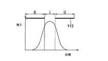
前記基板の上部に設けられ、前記ビーム拡大部で拡大されたビームの中心領域の最大強さの半分になる地点までを通過させ、残りの領域を遮断するビーム遮断部と、
前記基板の下部に設けられ、前記基板を上下左右方向へ移送させる基板移送装置と、
を備えることを特徴とするナノパターン形成装置。 - 前記レーザと前記ビームスプリッタとの間に、前記レーザから発せられたビームの経路を変える反射鏡を、さらに備えたことを特徴とする請求項1に記載のナノパターン形成装置。
- 前記ビーム遮断部が、拡大されたビームの中心領域区間のみを通過させるよう、その中心部に透過部を設けてなることを特徴とする請求項1に記載のナノパターン形成装置。
- レーザからビームを発生させるステップと、
ビームスプリッタによって、前記ビームを強さが同一の二つのビームに分けるステップと、
可変鏡によって、前記二つのビームを基板に向けるステップと、
前記基板に向けて進む二つのビームの進み経路に各々位置するビーム拡大部によって、前記ビームの直径を拡大させるステップと、
前記基板に前記拡大されたビームを照射するが、前記基板の上部に備えられたビーム遮断部の中心部に形成された透過部によって、前記拡大されたビームの強さが均一な中心領域の最大強さの半分になる地点までのみを通過させて前記基板に局部的な単位パターンを形成するステップと、
前記基板の下部に備えられた基板移送装置を上下左右方向に前記単位パターンの大きさ分だけ移動させて先に形成された単位パターンと連結される他の単位パターンを連続的に形成するステップと、
を含み、前記単位パターンを形成するステップを繰り返して上記基板全体に区間別に均一性を有するパターンを形成することを特徴とするナノパターン形成方法。 - 前記基板に紫外線硬化性樹脂が塗布されていることを特徴とする請求項4に記載のナノパターン形成方法。
- 少なくとも一つ以上の反射鏡にて、前記レーザから発せられたビームの経路を変えるステップを、さらに含むことを特徴とする請求項4に記載のナノパターン形成方法。
Applications Claiming Priority (2)
| Application Number | Priority Date | Filing Date | Title |
|---|---|---|---|
| KR1020070080268A KR100881140B1 (ko) | 2007-08-09 | 2007-08-09 | 나노패턴 형성장치 및 이를 이용한 나노패턴 형성방법 |
| KR10-2007-0080268 | 2007-08-09 |
Publications (2)
| Publication Number | Publication Date |
|---|---|
| JP2009044158A JP2009044158A (ja) | 2009-02-26 |
| JP5000603B2 true JP5000603B2 (ja) | 2012-08-15 |
Family
ID=39864672
Family Applications (1)
| Application Number | Title | Priority Date | Filing Date |
|---|---|---|---|
| JP2008204695A Active JP5000603B2 (ja) | 2007-08-09 | 2008-08-07 | ナノパターン形成装置及びこれを用いたナノパターン形成方法 |
Country Status (4)
| Country | Link |
|---|---|
| US (1) | US8198609B2 (ja) |
| EP (1) | EP2023205B1 (ja) |
| JP (1) | JP5000603B2 (ja) |
| KR (1) | KR100881140B1 (ja) |
Families Citing this family (16)
| Publication number | Priority date | Publication date | Assignee | Title |
|---|---|---|---|---|
| JP2013026283A (ja) * | 2011-07-15 | 2013-02-04 | Toshiba Corp | 干渉露光装置 |
| JP2013130649A (ja) * | 2011-12-20 | 2013-07-04 | Dexerials Corp | 干渉露光装置及び干渉露光方法 |
| KR101902267B1 (ko) | 2012-02-17 | 2018-09-28 | 삼성전자주식회사 | 나노 스케일 공진기, 나노 스케일 센서 및 이의 제조방법 |
| KR101356204B1 (ko) * | 2012-05-14 | 2014-01-27 | 주식회사 이엔씨 테크놀로지 | 라인 레이져 모듈 |
| CN103084737B (zh) * | 2012-09-27 | 2015-05-13 | 北京工业大学 | 一种采用超快激光在靶材表面制备纳米栅格的方法及装置 |
| KR101959334B1 (ko) | 2013-01-09 | 2019-03-19 | 삼성전자주식회사 | 레이저 간섭 리소그래피를 이용한 나노 공진기 제작 장치 및 방법 |
| CN105612611B (zh) * | 2013-08-09 | 2019-03-12 | 科磊股份有限公司 | 用于提高检测灵敏度的多点照明 |
| KR101527002B1 (ko) * | 2013-11-18 | 2015-06-09 | 주식회사 유알테크놀로지 | 레이저빔 발생장치 |
| JP6221849B2 (ja) * | 2014-03-07 | 2017-11-01 | ウシオ電機株式会社 | 露光方法、微細周期構造体の製造方法、グリッド偏光素子の製造方法及び露光装置 |
| JP6528394B2 (ja) * | 2014-12-02 | 2019-06-12 | ウシオ電機株式会社 | 基板上構造体の製造方法 |
| JP2017054006A (ja) * | 2015-09-09 | 2017-03-16 | ウシオ電機株式会社 | 光照射方法、基板上構造体の製造方法および基板上構造体 |
| US10101652B2 (en) | 2015-09-24 | 2018-10-16 | Ushio Denki Kabushiki Kaisha | Exposure method, method of fabricating periodic microstructure, method of fabricating grid polarizing element and exposure apparatus |
| JP6953109B2 (ja) * | 2015-09-24 | 2021-10-27 | ウシオ電機株式会社 | 基板上構造体の製造方法 |
| CN105446089B (zh) * | 2015-12-29 | 2017-09-29 | 中国科学技术大学 | 数字微镜设备与多面棱镜结合的多光束干涉光刻方法 |
| CN106707389B (zh) * | 2016-12-30 | 2019-05-31 | 浙江大学 | 一种渐变体全息光栅及其制作方法与装置 |
| CN110346857A (zh) * | 2019-07-15 | 2019-10-18 | 英诺激光科技股份有限公司 | 利用多束超快激光制作衍射光学器件的方法 |
Family Cites Families (22)
| Publication number | Priority date | Publication date | Assignee | Title |
|---|---|---|---|---|
| JPS5983111A (ja) | 1982-11-04 | 1984-05-14 | Sumitomo Electric Ind Ltd | 光集積回路作製法 |
| JP3296448B2 (ja) * | 1993-03-15 | 2002-07-02 | 株式会社ニコン | 露光制御方法、走査露光方法、露光制御装置、及びデバイス製造方法 |
| JPH06300909A (ja) | 1993-04-13 | 1994-10-28 | Canon Inc | ホログラフィック干渉露光法を用いた回折格子作成方法及びこれを用いた光半導体装置 |
| JP3564215B2 (ja) | 1995-11-30 | 2004-09-08 | シャープ株式会社 | 干渉露光装置およびそれを用いた干渉露光方法 |
| JP3646782B2 (ja) * | 1999-12-14 | 2005-05-11 | 株式会社村田製作所 | アンテナ装置およびそれを用いた通信機 |
| US7304775B2 (en) * | 2000-03-03 | 2007-12-04 | Coho Holdings, Llc | Actively stabilized, single input beam, interference lithography system and method |
| JP4258958B2 (ja) | 2000-07-10 | 2009-04-30 | コニカミノルタオプト株式会社 | 偏光位相変調素子の製造方法及び製造装置 |
| KR100478757B1 (ko) * | 2002-04-17 | 2005-03-24 | 엘지.필립스 엘시디 주식회사 | 실리콘 결정화방법 |
| US8110345B2 (en) | 2002-12-04 | 2012-02-07 | Taiwan Semiconductor Manufacturing Company, Ltd. | High resolution lithography system and method |
| JP2004294756A (ja) | 2003-03-27 | 2004-10-21 | Tdk Corp | 空間光変調器及びホログラム記録再生装置 |
| JP4239082B2 (ja) | 2003-09-26 | 2009-03-18 | 日本電信電話株式会社 | 周期配列構造のパターン形成方法および形成装置 |
| US7228034B2 (en) * | 2003-11-03 | 2007-06-05 | Intel Corporation | Interference patterning |
| TWI229750B (en) | 2003-11-28 | 2005-03-21 | Ind Tech Res Inst | Manufacturing device of micro-grating component |
| US7088482B2 (en) * | 2004-02-10 | 2006-08-08 | Imation Corp. | Holographic recording techniques using first and second portions of a spatial light modulator |
| CN1926934A (zh) | 2004-03-29 | 2007-03-07 | 仲田涂覆株式会社 | 覆膜铁氧体成形品及覆膜铁氧体成形品的制造方法 |
| JP4389791B2 (ja) | 2004-08-25 | 2009-12-24 | セイコーエプソン株式会社 | 微細構造体の製造方法および露光装置 |
| US7751030B2 (en) | 2005-02-01 | 2010-07-06 | Asml Holding N.V. | Interferometric lithographic projection apparatus |
| JP2006259519A (ja) | 2005-03-18 | 2006-09-28 | Fujitsu Ltd | ホログラム記録装置 |
| KR100878433B1 (ko) * | 2005-05-18 | 2009-01-13 | 삼성전기주식회사 | 발광소자의 오믹컨택층 제조방법 및 이를 이용한발광소자의 제조방법 |
| US20070077498A1 (en) * | 2005-09-30 | 2007-04-05 | Fuji Photo Film Co., Ltd. | Optical recording composition, optical recording medium and production method thereof, optical recording method and optical recording apparatus |
| US7440078B2 (en) | 2005-12-20 | 2008-10-21 | Asml Netherlands B.V. | Lithographic apparatus and device manufacturing method using interferometric and maskless exposure units |
| US20080241706A1 (en) * | 2007-03-30 | 2008-10-02 | Industrial Technology Research Institute | Holographic data storage medium and fabrication method thereof |
-
2007
- 2007-08-09 KR KR1020070080268A patent/KR100881140B1/ko active Active
-
2008
- 2008-07-17 EP EP08012920A patent/EP2023205B1/en active Active
- 2008-07-23 US US12/219,547 patent/US8198609B2/en active Active
- 2008-08-07 JP JP2008204695A patent/JP5000603B2/ja active Active
Also Published As
| Publication number | Publication date |
|---|---|
| EP2023205B1 (en) | 2012-09-12 |
| EP2023205A2 (en) | 2009-02-11 |
| EP2023205A3 (en) | 2011-01-05 |
| KR100881140B1 (ko) | 2009-02-02 |
| US20090039293A1 (en) | 2009-02-12 |
| JP2009044158A (ja) | 2009-02-26 |
| US8198609B2 (en) | 2012-06-12 |
Similar Documents
| Publication | Publication Date | Title |
|---|---|---|
| JP5000603B2 (ja) | ナノパターン形成装置及びこれを用いたナノパターン形成方法 | |
| Emami et al. | An analytical model for scanning-projection based stereolithography | |
| JP7345769B2 (ja) | 直接描画露光システム及び直接描画露光方法 | |
| JP2016021049A (ja) | 光照射装置および描画装置 | |
| US20160109806A1 (en) | Illumination device and method for using the same in the projection lithography machine | |
| CN112596347A (zh) | 一种数字掩膜投影光刻的多重曝光方法 | |
| JP2024533571A (ja) | 3次元コンポーネントのリソグラフィ・ベースの生成的製造のための方法及び装置 | |
| JP2005531797A (ja) | 光作用感応構造の書き込み | |
| KR20140120697A (ko) | Glv를 이용한 디지털 노광기 및 dmd를 이용한 디지털 노광기 | |
| CN102929106B (zh) | 用于紫外光刻机的光刻照明系统 | |
| Haq et al. | Vertical sidewalls in thick epoxy resists–a challenge for laser-based direct write lithography | |
| WO2018062008A1 (ja) | 三次元造形装置、三次元物体製造方法および三次元造形プログラム | |
| KR20200068580A (ko) | 프레임 경화 템플릿 및 프레임 경화 템플릿 이용 시스템 및 방법 | |
| JP4477893B2 (ja) | レーザ加工方法及び装置、並びに、レーザ加工方法を使用した構造体の製造方法 | |
| KR20220148321A (ko) | 연속 회절 광학 소자를 생성하기 위한 방법, 생성 방법을 수행하기 위한 장치, 및 연속 회절 광학 소자 | |
| US8585390B2 (en) | Mold making system and mold making method | |
| CN103472688B (zh) | 深紫外投影光刻机的照明装置及使用方法 | |
| US10866520B2 (en) | Light irradiation method | |
| JP6547283B2 (ja) | 基板上構造体の製造方法 | |
| JP2002292488A (ja) | レーザ加工装置とレーザ加工方法 | |
| KR20210021966A (ko) | 이미지 포인트 노출 방법 및 장치 | |
| KR101318941B1 (ko) | 레이저 간섭 리소그라피 장치 | |
| CN101273304A (zh) | 用于光刻设备的照射器 | |
| KR101229786B1 (ko) | 헤테로다인 간섭 리소그래피 장치, 그 장치를 이용한 미세패턴 형성방법, 웨이퍼 및 반도체 소자 | |
| CN101344726B (zh) | 制作周期性图案的步进排列式干涉微影方法及其装置 |
Legal Events
| Date | Code | Title | Description |
|---|---|---|---|
| RD02 | Notification of acceptance of power of attorney |
Free format text: JAPANESE INTERMEDIATE CODE: A7422 Effective date: 20091126 |
|
| RD02 | Notification of acceptance of power of attorney |
Free format text: JAPANESE INTERMEDIATE CODE: A7422 Effective date: 20100107 |
|
| RD04 | Notification of resignation of power of attorney |
Free format text: JAPANESE INTERMEDIATE CODE: A7424 Effective date: 20100108 |
|
| A711 | Notification of change in applicant |
Free format text: JAPANESE INTERMEDIATE CODE: A711 Effective date: 20100714 |
|
| A521 | Request for written amendment filed |
Free format text: JAPANESE INTERMEDIATE CODE: A523 Effective date: 20100827 |
|
| A131 | Notification of reasons for refusal |
Free format text: JAPANESE INTERMEDIATE CODE: A131 Effective date: 20110125 |
|
| A521 | Request for written amendment filed |
Free format text: JAPANESE INTERMEDIATE CODE: A523 Effective date: 20110411 |
|
| A131 | Notification of reasons for refusal |
Free format text: JAPANESE INTERMEDIATE CODE: A131 Effective date: 20110614 |
|
| A521 | Request for written amendment filed |
Free format text: JAPANESE INTERMEDIATE CODE: A523 Effective date: 20110914 |
|
| A02 | Decision of refusal |
Free format text: JAPANESE INTERMEDIATE CODE: A02 Effective date: 20111122 |
|
| A521 | Request for written amendment filed |
Free format text: JAPANESE INTERMEDIATE CODE: A523 Effective date: 20120321 |
|
| A911 | Transfer to examiner for re-examination before appeal (zenchi) |
Free format text: JAPANESE INTERMEDIATE CODE: A911 Effective date: 20120329 |
|
| TRDD | Decision of grant or rejection written | ||
| A01 | Written decision to grant a patent or to grant a registration (utility model) |
Free format text: JAPANESE INTERMEDIATE CODE: A01 Effective date: 20120417 |
|
| A01 | Written decision to grant a patent or to grant a registration (utility model) |
Free format text: JAPANESE INTERMEDIATE CODE: A01 |
|
| A61 | First payment of annual fees (during grant procedure) |
Free format text: JAPANESE INTERMEDIATE CODE: A61 Effective date: 20120516 |
|
| R150 | Certificate of patent or registration of utility model |
Ref document number: 5000603 Country of ref document: JP Free format text: JAPANESE INTERMEDIATE CODE: R150 Free format text: JAPANESE INTERMEDIATE CODE: R150 |
|
| FPAY | Renewal fee payment (event date is renewal date of database) |
Free format text: PAYMENT UNTIL: 20150525 Year of fee payment: 3 |
|
| FPAY | Renewal fee payment (event date is renewal date of database) |
Free format text: PAYMENT UNTIL: 20150525 Year of fee payment: 3 |
|
| S111 | Request for change of ownership or part of ownership |
Free format text: JAPANESE INTERMEDIATE CODE: R313111 |
|
| S631 | Written request for registration of reclamation of domicile |
Free format text: JAPANESE INTERMEDIATE CODE: R313631 |
|
| FPAY | Renewal fee payment (event date is renewal date of database) |
Free format text: PAYMENT UNTIL: 20150525 Year of fee payment: 3 |
|
| R371 | Transfer withdrawn |
Free format text: JAPANESE INTERMEDIATE CODE: R371 |
|
| S111 | Request for change of ownership or part of ownership |
Free format text: JAPANESE INTERMEDIATE CODE: R313111 |
|
| S631 | Written request for registration of reclamation of domicile |
Free format text: JAPANESE INTERMEDIATE CODE: R313631 |
|
| S633 | Written request for registration of reclamation of name |
Free format text: JAPANESE INTERMEDIATE CODE: R313633 |
|
| FPAY | Renewal fee payment (event date is renewal date of database) |
Free format text: PAYMENT UNTIL: 20150525 Year of fee payment: 3 |
|
| R371 | Transfer withdrawn |
Free format text: JAPANESE INTERMEDIATE CODE: R371 |
|
| FPAY | Renewal fee payment (event date is renewal date of database) |
Free format text: PAYMENT UNTIL: 20150525 Year of fee payment: 3 |
|
| S111 | Request for change of ownership or part of ownership |
Free format text: JAPANESE INTERMEDIATE CODE: R313111 |
|
| S531 | Written request for registration of change of domicile |
Free format text: JAPANESE INTERMEDIATE CODE: R313531 |
|
| S533 | Written request for registration of change of name |
Free format text: JAPANESE INTERMEDIATE CODE: R313533 |
|
| FPAY | Renewal fee payment (event date is renewal date of database) |
Free format text: PAYMENT UNTIL: 20150525 Year of fee payment: 3 |
|
| R350 | Written notification of registration of transfer |
Free format text: JAPANESE INTERMEDIATE CODE: R350 |
|
| R250 | Receipt of annual fees |
Free format text: JAPANESE INTERMEDIATE CODE: R250 |
|
| R250 | Receipt of annual fees |
Free format text: JAPANESE INTERMEDIATE CODE: R250 |
|
| R250 | Receipt of annual fees |
Free format text: JAPANESE INTERMEDIATE CODE: R250 |
|
| R250 | Receipt of annual fees |
Free format text: JAPANESE INTERMEDIATE CODE: R250 |
|
| R250 | Receipt of annual fees |
Free format text: JAPANESE INTERMEDIATE CODE: R250 |
|
| R250 | Receipt of annual fees |
Free format text: JAPANESE INTERMEDIATE CODE: R250 |
|
| R250 | Receipt of annual fees |
Free format text: JAPANESE INTERMEDIATE CODE: R250 |
|
| R250 | Receipt of annual fees |
Free format text: JAPANESE INTERMEDIATE CODE: R250 |
|
| R250 | Receipt of annual fees |
Free format text: JAPANESE INTERMEDIATE CODE: R250 |
|
| R250 | Receipt of annual fees |
Free format text: JAPANESE INTERMEDIATE CODE: R250 |
|
| R250 | Receipt of annual fees |
Free format text: JAPANESE INTERMEDIATE CODE: R250 |