JP5072025B2 - 半導体装置の製造方法 - Google Patents
半導体装置の製造方法 Download PDFInfo
- Publication number
- JP5072025B2 JP5072025B2 JP2007556865A JP2007556865A JP5072025B2 JP 5072025 B2 JP5072025 B2 JP 5072025B2 JP 2007556865 A JP2007556865 A JP 2007556865A JP 2007556865 A JP2007556865 A JP 2007556865A JP 5072025 B2 JP5072025 B2 JP 5072025B2
- Authority
- JP
- Japan
- Prior art keywords
- light
- semiconductor
- semiconductor substrate
- manufacturing
- semiconductor device
- Prior art date
- Legal status (The legal status is an assumption and is not a legal conclusion. Google has not performed a legal analysis and makes no representation as to the accuracy of the status listed.)
- Active
Links
Images




Classifications
-
- H—ELECTRICITY
- H10—SEMICONDUCTOR DEVICES; ELECTRIC SOLID-STATE DEVICES NOT OTHERWISE PROVIDED FOR
- H10P—GENERIC PROCESSES OR APPARATUS FOR THE MANUFACTURE OR TREATMENT OF DEVICES COVERED BY CLASS H10
- H10P50/00—Etching of wafers, substrates or parts of devices
-
- H—ELECTRICITY
- H10—SEMICONDUCTOR DEVICES; ELECTRIC SOLID-STATE DEVICES NOT OTHERWISE PROVIDED FOR
- H10P—GENERIC PROCESSES OR APPARATUS FOR THE MANUFACTURE OR TREATMENT OF DEVICES COVERED BY CLASS H10
- H10P70/00—Cleaning of wafers, substrates or parts of devices
- H10P70/10—Cleaning before device manufacture, i.e. Begin-Of-Line process
- H10P70/15—Cleaning before device manufacture, i.e. Begin-Of-Line process by wet cleaning only
-
- H—ELECTRICITY
- H10—SEMICONDUCTOR DEVICES; ELECTRIC SOLID-STATE DEVICES NOT OTHERWISE PROVIDED FOR
- H10P—GENERIC PROCESSES OR APPARATUS FOR THE MANUFACTURE OR TREATMENT OF DEVICES COVERED BY CLASS H10
- H10P70/00—Cleaning of wafers, substrates or parts of devices
- H10P70/20—Cleaning during device manufacture
- H10P70/27—Cleaning during device manufacture during, before or after processing of conductive materials, e.g. polysilicon or amorphous silicon layers
- H10P70/277—Cleaning during device manufacture during, before or after processing of conductive materials, e.g. polysilicon or amorphous silicon layers the processing being a planarisation of conductive layers
Landscapes
- Cleaning Or Drying Semiconductors (AREA)
- Weting (AREA)
- Electrodes Of Semiconductors (AREA)
Description
実施の形態1では、半導体デバイス製造に本発明の処理方法が使用される場合の形態について説明する。
以下に、本発明の具体的態様を説明するが、本発明はその要旨を越えない限り以下の実施例により何ら限定されるものではない。
シリコンウェーハを、超純水で処理する際のシリコン表面の酸化抑制について、本発明の効果を検証した。シリコンウェーハは(CZ法、nタイプ、抵抗率:0.8〜1.2Ωcm、面方位:100)とし、あらかじめ硫酸/過酸化水素水で洗浄した後、希フッ酸処理(0.5%、室温、1分間)によって、表面の酸化膜を除去し、その後、超純水で5分間リンスしたものを使用した。
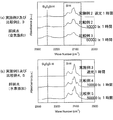
図5(a)では、シリコンウェーハを、空気が飽和した超純水に1時間浸漬した後の表面状態を、光の強度を変えて比較している。
図5(b)では、溶存酸素濃度1ppb以下、1.3-1.5ppmの水素を添加した超純水を用いて、シリコンウェーハを1時間浸漬した後の表面状態を、光の強度を変えて比較している。
シリコンウェーハをアンモニア水で表面処理した場合における表面マイクロラフネス抑制について、本発明の効果を検証した。実験条件並びに結果を表1に示す。

シリコンウェーハを超純水で表面処理した場合における表面マイクロラフネス抑制について、本発明の効果を検証した。実験条件並びに結果を表2に示す。
シリコンウェーハをフッ酸並びにバッファードフッ酸で表面処理した場合の、表面マイクロラフネスについて、本発明の効果を検証した。実験条件並びに結果を表3に示す。
シリコンウェーハを表4に示す各種薬液で表面処理した場合の、表面マイクロラフネスについて、本発明の効果を検証した。実験条件並びに結果を表4に示す。
Claims (8)
- 半導体基板を用意してその表面をウエット洗浄し、該洗浄した表面上に絶縁膜を形成し、該形成した絶縁膜をウエットエッチングしてゲート絶縁膜を形成し、その後再度ウエット洗浄する工程を有する半導体装置の製造方法であって、
ウエット洗浄工程、ウエットエッチング工程、再度のウエット洗浄工程の各工程を遮光下の環境で実施することにより、前記ウエット洗浄工程、ウエットエッチング工程、及び再度のウエット洗浄工程の各工程における前記半導体基板の表面ラフネスを、前記各工程を遮光しない状態で実施した場合に比較して、抑制することを特徴とする半導体装置の製造方法。 - 前記3つの工程のそれぞれで使用される処理液中の酸素濃度が1ppb以下である請求項1記載の半導体装置の製造方法。
- 前記遮光下の環境の雰囲気が窒素雰囲気である請求項1記載の半導体装置の製造方法。
- 前記半導体基板はシリコンウエハーであり、遮光する光の波長は、1.1μm以下である請求項1の半導体装置の製造方法。
- 半導体基板を洗浄し、洗浄された半導体基板上に形成された絶縁膜をエッチングした後、再度洗浄する工程を液に曝して行い、ゲート絶縁膜を形成する半導体装置の製造方法であって、
前記半導体基板の洗浄工程、前記絶縁膜のエッチング工程、及び再度洗浄する工程の各工程を、前記半導体基板表面に光があたらないように遮光して行うことにより、前記半導体基板の洗浄工程、前記絶縁膜のエッチング工程、及び再度洗浄する工程の各工程における前記半導体基板の表面ラフネスを、前記各工程を遮光しない場合に比較して抑制した状態で、前記ゲート絶縁膜を形成することを特徴とする半導体装置の製造方法。 - 前記半導体基板の洗浄、前記絶縁膜のエッチング、及び再度洗浄する工程は、前記半導体基板表面に光があたらないように遮光した処理室内で行われることを特徴とする請求項5記載の半導体装置の製造方法。
- 前記遮光される光は、前記半導体基板を形成する半導体のバンドギャップエネルギ以上のエネルギを有する光であることを特徴とする請求項5又は6に記載の半導体装置の製造方法。
- 前記半導体基板の半導体がシリコンであり、前記遮光される光が可視光、紫外線であることを特徴とする請求項5〜7のいずれか一項に記載の半導体装置の製造方法。
Priority Applications (1)
| Application Number | Priority Date | Filing Date | Title |
|---|---|---|---|
| JP2007556865A JP5072025B2 (ja) | 2006-02-01 | 2007-01-30 | 半導体装置の製造方法 |
Applications Claiming Priority (4)
| Application Number | Priority Date | Filing Date | Title |
|---|---|---|---|
| JP2006024755 | 2006-02-01 | ||
| JP2006024755 | 2006-02-01 | ||
| PCT/JP2007/051487 WO2007088848A1 (ja) | 2006-02-01 | 2007-01-30 | 半導体装置の製造方法及び半導体表面のマイクロラフネス低減方法 |
| JP2007556865A JP5072025B2 (ja) | 2006-02-01 | 2007-01-30 | 半導体装置の製造方法 |
Publications (2)
| Publication Number | Publication Date |
|---|---|
| JPWO2007088848A1 JPWO2007088848A1 (ja) | 2009-06-25 |
| JP5072025B2 true JP5072025B2 (ja) | 2012-11-14 |
Family
ID=38327420
Family Applications (1)
| Application Number | Title | Priority Date | Filing Date |
|---|---|---|---|
| JP2007556865A Active JP5072025B2 (ja) | 2006-02-01 | 2007-01-30 | 半導体装置の製造方法 |
Country Status (7)
| Country | Link |
|---|---|
| US (2) | US8268735B2 (ja) |
| EP (1) | EP1988567B1 (ja) |
| JP (1) | JP5072025B2 (ja) |
| KR (1) | KR101070204B1 (ja) |
| CN (1) | CN101379597B (ja) |
| TW (1) | TWI404134B (ja) |
| WO (1) | WO2007088848A1 (ja) |
Families Citing this family (24)
| Publication number | Priority date | Publication date | Assignee | Title |
|---|---|---|---|---|
| AU2003264642B2 (en) * | 2002-12-02 | 2009-08-06 | Tadahiro Ohmi | Semiconductor Device and Method of Manufacturing the Same |
| JP4973469B2 (ja) * | 2007-11-30 | 2012-07-11 | 岩崎電気株式会社 | 活性酸素種の検出方法及び検出装置 |
| US8404626B2 (en) * | 2007-12-21 | 2013-03-26 | Lam Research Corporation | Post-deposition cleaning methods and formulations for substrates with cap layers |
| DE102008056455B3 (de) * | 2008-11-07 | 2010-04-29 | Centrotherm Photovoltaics Technology Gmbh | Oxidations- und Reinigungsverfahren für Siliziumscheiben |
| US20120100721A1 (en) * | 2009-06-25 | 2012-04-26 | Lam Research Ag | Method for treating a semiconductor wafer |
| US20110081771A1 (en) * | 2009-10-07 | 2011-04-07 | Applied Materials, Inc. | Multichamber split processes for led manufacturing |
| WO2012002440A1 (ja) * | 2010-06-29 | 2012-01-05 | 京セラ株式会社 | 半導体基板の表面処理方法、半導体基板、および太陽電池の製造方法 |
| JP6300139B2 (ja) * | 2012-05-15 | 2018-03-28 | 株式会社Screenホールディングス | 基板処理方法および基板処理システム |
| JP5911757B2 (ja) * | 2012-06-08 | 2016-04-27 | ソニー株式会社 | 基板処理方法、基板処理装置、および記録媒体 |
| US20140196744A1 (en) * | 2013-01-11 | 2014-07-17 | Taiwan Semiconductor Manufacturing Company, Ltd. | Method and device for cleaning a brush surface having a contamination |
| CN105340067B (zh) * | 2013-04-30 | 2018-07-06 | 奥加诺株式会社 | 铜露出基板的清洗方法和清洗系统 |
| JP2014225570A (ja) * | 2013-05-16 | 2014-12-04 | 栗田工業株式会社 | デバイス用Ge基板の洗浄方法、洗浄水供給装置及び洗浄装置 |
| US9224734B2 (en) * | 2013-09-13 | 2015-12-29 | Taiwan Semiconductor Manufacturing Company, Ltd. | CMOS devices with reduced leakage and methods of forming the same |
| WO2015189933A1 (ja) * | 2014-06-11 | 2015-12-17 | 栗田工業株式会社 | デバイス用Ge基板の洗浄方法、洗浄水供給装置及び洗浄装置 |
| CN105576074A (zh) * | 2014-10-08 | 2016-05-11 | 上海神舟新能源发展有限公司 | 一种n型双面电池的湿法刻蚀方法 |
| JP6348994B2 (ja) * | 2015-02-12 | 2018-06-27 | 富士フイルム株式会社 | Iii−v族元素の酸化物の除去液および除去方法、iii−v族元素の化合物の処理液、iii−v族元素の酸化防止液、ならびに、半導体基板の処理液および半導体基板製品の製造方法 |
| JP6020626B2 (ja) * | 2015-03-06 | 2016-11-02 | 栗田工業株式会社 | デバイス用Ge基板の洗浄方法、洗浄水供給装置及び洗浄装置 |
| JP6917807B2 (ja) * | 2017-07-03 | 2021-08-11 | 東京エレクトロン株式会社 | 基板処理方法 |
| CN107634006A (zh) * | 2017-09-12 | 2018-01-26 | 武汉新芯集成电路制造有限公司 | 晶圆的返工方法 |
| JP7219947B2 (ja) * | 2018-05-22 | 2023-02-09 | 国立大学法人九州工業大学 | 表面処理方法 |
| JP6996488B2 (ja) * | 2018-12-26 | 2022-01-17 | 株式会社Sumco | シリコンウェーハのバッチ式洗浄方法並びにその洗浄方法を用いたシリコンウェーハの製造方法及びシリコンウェーハの洗浄条件決定方法 |
| US12012575B2 (en) * | 2019-03-26 | 2024-06-18 | Fujimi Incorporated | Composition for surface treatment, method for producing the same, surface treatment method, and method for producing semiconductor substrate |
| JP7821478B2 (ja) * | 2021-12-27 | 2026-02-27 | 国立大学法人九州工業大学 | 基板の表面処理方法、表面処理装置および表面処理溶液 |
| CN116525432B (zh) * | 2023-06-29 | 2023-09-22 | 合肥晶合集成电路股份有限公司 | 半导体器件的刻蚀方法及制备方法 |
Citations (6)
| Publication number | Priority date | Publication date | Assignee | Title |
|---|---|---|---|---|
| JP2002083796A (ja) * | 2000-09-08 | 2002-03-22 | Mitsubishi Electric Corp | 半導体装置の製造方法およびこれに用いる製造装置 |
| JP2003234341A (ja) * | 2001-09-21 | 2003-08-22 | Dainippon Screen Mfg Co Ltd | 基板処理装置 |
| JP2004119714A (ja) * | 2002-09-26 | 2004-04-15 | Dainippon Screen Mfg Co Ltd | 基板処理装置 |
| JP2004296997A (ja) * | 2003-03-28 | 2004-10-21 | Renesas Technology Corp | 半導体集積回路装置の製造方法 |
| JP2005045206A (ja) * | 2003-07-07 | 2005-02-17 | Dainippon Screen Mfg Co Ltd | 基板処理方法および基板処理装置 |
| JP2005093562A (ja) * | 2003-09-12 | 2005-04-07 | Tadahiro Omi | 半導体装置の製造方法 |
Family Cites Families (18)
| Publication number | Priority date | Publication date | Assignee | Title |
|---|---|---|---|---|
| GB1020328A (en) * | 1964-12-11 | 1966-02-16 | Standard Telephones Cables Ltd | Processing of semiconductor devices |
| US5250471A (en) * | 1988-12-26 | 1993-10-05 | The Furukawa Electric Co. | Method for manufacturing compound semiconductor devices including a step where the semiconductor is etched without exposure to light |
| DE4031676A1 (de) * | 1990-10-04 | 1992-04-09 | Hahn Meitner Kernforsch | Verfahren zum behandeln der oberflaeche eines siliziumkoerpers |
| KR100203781B1 (ko) * | 1996-09-13 | 1999-06-15 | 윤종용 | 반도체 포토리소그래피 공정의 현상액 공급시스템 |
| US6153043A (en) * | 1998-02-06 | 2000-11-28 | International Business Machines Corporation | Elimination of photo-induced electrochemical dissolution in chemical mechanical polishing |
| US6361614B1 (en) * | 1999-04-21 | 2002-03-26 | Agere Systems Guardian Corp. | Dark spin rinse/dry |
| DE10020363A1 (de) * | 2000-04-26 | 2001-10-31 | Kunkel Klaus | Verfahren zum Betreiben eines Antriebes |
| WO2002089192A1 (en) * | 2001-04-27 | 2002-11-07 | Koninklijke Philips Electronics N.V. | Method of wet etching an inorganic antireflection layer |
| US20030015731A1 (en) * | 2001-07-23 | 2003-01-23 | Motorola, Inc. | Process for fabricating semiconductor structures and devices utilizing the formation of a compliant substrate used to form the same and in-situ annealing |
| US20030154999A1 (en) * | 2002-02-20 | 2003-08-21 | Taiwan Semiconductor Manufacturing Co., Ltd. | Method for preventing chemical attack on a copper containing semiconductor wafer |
| US20040060582A1 (en) | 2002-09-18 | 2004-04-01 | Dainippon Screen Mfg.Co., Ltd. | Substrate processing apparatus |
| AU2003264642B2 (en) * | 2002-12-02 | 2009-08-06 | Tadahiro Ohmi | Semiconductor Device and Method of Manufacturing the Same |
| EP1434281A3 (en) * | 2002-12-26 | 2007-10-24 | Konica Minolta Holdings, Inc. | Manufacturing method of thin-film transistor, thin-film transistor sheet, and electric circuit |
| JP4336530B2 (ja) * | 2003-06-26 | 2009-09-30 | 株式会社ルネサステクノロジ | ウエット処理装置、ウエット処理方法および半導体装置の製造方法 |
| US20060011224A1 (en) * | 2004-07-18 | 2006-01-19 | Chung-Chih Chen | Extrusion free wet cleaning process |
| US7232759B2 (en) * | 2004-10-04 | 2007-06-19 | Applied Materials, Inc. | Ammonium hydroxide treatments for semiconductor substrates |
| JP5116482B2 (ja) * | 2005-11-14 | 2013-01-09 | 帝國製薬株式会社 | イオントフォレーシス用製剤 |
| US7288458B2 (en) * | 2005-12-14 | 2007-10-30 | Freescale Semiconductor, Inc. | SOI active layer with different surface orientation |
-
2007
- 2007-01-30 CN CN2007800041052A patent/CN101379597B/zh not_active Expired - Fee Related
- 2007-01-30 EP EP07707705.5A patent/EP1988567B1/en not_active Expired - Fee Related
- 2007-01-30 WO PCT/JP2007/051487 patent/WO2007088848A1/ja not_active Ceased
- 2007-01-30 KR KR1020087019229A patent/KR101070204B1/ko active Active
- 2007-01-30 US US12/223,385 patent/US8268735B2/en active Active
- 2007-01-30 JP JP2007556865A patent/JP5072025B2/ja active Active
- 2007-02-01 TW TW096103652A patent/TWI404134B/zh active
-
2012
- 2012-08-31 US US13/601,157 patent/US20120329284A1/en not_active Abandoned
Patent Citations (6)
| Publication number | Priority date | Publication date | Assignee | Title |
|---|---|---|---|---|
| JP2002083796A (ja) * | 2000-09-08 | 2002-03-22 | Mitsubishi Electric Corp | 半導体装置の製造方法およびこれに用いる製造装置 |
| JP2003234341A (ja) * | 2001-09-21 | 2003-08-22 | Dainippon Screen Mfg Co Ltd | 基板処理装置 |
| JP2004119714A (ja) * | 2002-09-26 | 2004-04-15 | Dainippon Screen Mfg Co Ltd | 基板処理装置 |
| JP2004296997A (ja) * | 2003-03-28 | 2004-10-21 | Renesas Technology Corp | 半導体集積回路装置の製造方法 |
| JP2005045206A (ja) * | 2003-07-07 | 2005-02-17 | Dainippon Screen Mfg Co Ltd | 基板処理方法および基板処理装置 |
| JP2005093562A (ja) * | 2003-09-12 | 2005-04-07 | Tadahiro Omi | 半導体装置の製造方法 |
Also Published As
| Publication number | Publication date |
|---|---|
| KR20080090503A (ko) | 2008-10-08 |
| TW200741851A (en) | 2007-11-01 |
| EP1988567A4 (en) | 2009-12-02 |
| EP1988567B1 (en) | 2013-06-05 |
| US20090023231A1 (en) | 2009-01-22 |
| CN101379597A (zh) | 2009-03-04 |
| KR101070204B1 (ko) | 2011-10-06 |
| US20120329284A1 (en) | 2012-12-27 |
| US8268735B2 (en) | 2012-09-18 |
| EP1988567A1 (en) | 2008-11-05 |
| JPWO2007088848A1 (ja) | 2009-06-25 |
| TWI404134B (zh) | 2013-08-01 |
| CN101379597B (zh) | 2012-07-18 |
| WO2007088848A1 (ja) | 2007-08-09 |
Similar Documents
| Publication | Publication Date | Title |
|---|---|---|
| JP5072025B2 (ja) | 半導体装置の製造方法 | |
| US6696326B2 (en) | Cleaning method to prevent watermarks | |
| TWI520197B (zh) | Method of cleaning semiconductor wafers | |
| JP3679216B2 (ja) | 半導体基板の洗浄液及びこれを使用する洗浄方法 | |
| JP4162211B2 (ja) | シリコンウエハの洗浄方法および洗浄されたシリコンウエハ | |
| TW201624152A (zh) | 可抑制含鎢材料之損壞的半導體元件之清洗液及利用該清洗液的半導體元件之清洗方法 | |
| KR20170084008A (ko) | 탄탈을 포함하는 재료의 데미지를 억제한 반도체소자의 세정액, 및 이를 이용한 세정방법 | |
| US5803980A (en) | De-ionized water/ozone rinse post-hydrofluoric processing for the prevention of silicic acid residue | |
| US8288291B2 (en) | Method for removal of bulk metal contamination from III-V semiconductor substrates | |
| KR20100049856A (ko) | 기판 세정 방법 | |
| US6218085B1 (en) | Process for photoresist rework to avoid sodium incorporation | |
| JP2009260085A (ja) | 半導体装置の製造方法および半導体基板の洗浄方法 | |
| JP4857738B2 (ja) | 半導体ウエーハの洗浄方法および製造方法 | |
| TW202313946A (zh) | 後乾蝕刻光阻劑及含金屬殘留物的移除配方 | |
| KR100914606B1 (ko) | 습식 게이트 산화막 형성 방법 | |
| KR100604051B1 (ko) | 게이트 산화막의 전세정방법 | |
| JPH1079363A (ja) | 化合物半導体ウエハの表面処理方法 | |
| JP4758187B2 (ja) | フォトレジスト残渣及びポリマー残渣除去液 | |
| JP7279753B2 (ja) | シリコンウェーハの洗浄方法および製造方法 | |
| CN112652518A (zh) | 一种半导体器件的形成方法 | |
| JP2006016460A (ja) | Siを含有する基板の洗浄溶液及びSiを含有する基板の洗浄方法 | |
| KR100543016B1 (ko) | 박막트랜지스터의 제조 방법 | |
| KR100709564B1 (ko) | 반도체 소자 제조 방법 | |
| CN118006401A (zh) | 半导体器件的形成方法及清洗液 | |
| Fukazawa et al. | consumption and a simplified cleaning process can be established by this |
Legal Events
| Date | Code | Title | Description |
|---|---|---|---|
| A621 | Written request for application examination |
Free format text: JAPANESE INTERMEDIATE CODE: A621 Effective date: 20091112 |
|
| A131 | Notification of reasons for refusal |
Free format text: JAPANESE INTERMEDIATE CODE: A131 Effective date: 20111019 |
|
| A521 | Request for written amendment filed |
Free format text: JAPANESE INTERMEDIATE CODE: A523 Effective date: 20111214 |
|
| A02 | Decision of refusal |
Free format text: JAPANESE INTERMEDIATE CODE: A02 Effective date: 20120321 |
|
| A521 | Request for written amendment filed |
Free format text: JAPANESE INTERMEDIATE CODE: A523 Effective date: 20120618 |
|
| A911 | Transfer to examiner for re-examination before appeal (zenchi) |
Free format text: JAPANESE INTERMEDIATE CODE: A911 Effective date: 20120626 |
|
| TRDD | Decision of grant or rejection written | ||
| A01 | Written decision to grant a patent or to grant a registration (utility model) |
Free format text: JAPANESE INTERMEDIATE CODE: A01 Effective date: 20120725 |
|
| A01 | Written decision to grant a patent or to grant a registration (utility model) |
Free format text: JAPANESE INTERMEDIATE CODE: A01 |
|
| A61 | First payment of annual fees (during grant procedure) |
Free format text: JAPANESE INTERMEDIATE CODE: A61 Effective date: 20120817 |
|
| R150 | Certificate of patent or registration of utility model |
Ref document number: 5072025 Country of ref document: JP Free format text: JAPANESE INTERMEDIATE CODE: R150 Free format text: JAPANESE INTERMEDIATE CODE: R150 |
|
| FPAY | Renewal fee payment (event date is renewal date of database) |
Free format text: PAYMENT UNTIL: 20150831 Year of fee payment: 3 |
|
| R250 | Receipt of annual fees |
Free format text: JAPANESE INTERMEDIATE CODE: R250 |
|
| R250 | Receipt of annual fees |
Free format text: JAPANESE INTERMEDIATE CODE: R250 |
|
| R250 | Receipt of annual fees |
Free format text: JAPANESE INTERMEDIATE CODE: R250 |
|
| R250 | Receipt of annual fees |
Free format text: JAPANESE INTERMEDIATE CODE: R250 |
|
| R250 | Receipt of annual fees |
Free format text: JAPANESE INTERMEDIATE CODE: R250 |
|
| S111 | Request for change of ownership or part of ownership |
Free format text: JAPANESE INTERMEDIATE CODE: R313117 |
|
| R350 | Written notification of registration of transfer |
Free format text: JAPANESE INTERMEDIATE CODE: R350 |