JP5111012B2 - プラズマディスプレイ装置 - Google Patents
プラズマディスプレイ装置 Download PDFInfo
- Publication number
- JP5111012B2 JP5111012B2 JP2007211893A JP2007211893A JP5111012B2 JP 5111012 B2 JP5111012 B2 JP 5111012B2 JP 2007211893 A JP2007211893 A JP 2007211893A JP 2007211893 A JP2007211893 A JP 2007211893A JP 5111012 B2 JP5111012 B2 JP 5111012B2
- Authority
- JP
- Japan
- Prior art keywords
- conductive
- plasma display
- protective plate
- mesh
- layer
- Prior art date
- Legal status (The legal status is an assumption and is not a legal conclusion. Google has not performed a legal analysis and makes no representation as to the accuracy of the status listed.)
- Expired - Fee Related
Links
- 239000000463 material Substances 0.000 claims description 35
- 230000001681 protective effect Effects 0.000 claims description 25
- 239000011521 glass Substances 0.000 claims description 10
- 239000000758 substrate Substances 0.000 claims description 8
- 239000010410 layer Substances 0.000 description 23
- 238000000034 method Methods 0.000 description 15
- 239000012790 adhesive layer Substances 0.000 description 14
- 239000002585 base Substances 0.000 description 11
- 238000004519 manufacturing process Methods 0.000 description 8
- 238000010586 diagram Methods 0.000 description 7
- 230000002950 deficient Effects 0.000 description 5
- PXHVJJICTQNCMI-UHFFFAOYSA-N Nickel Chemical compound [Ni] PXHVJJICTQNCMI-UHFFFAOYSA-N 0.000 description 4
- KDLHZDBZIXYQEI-UHFFFAOYSA-N Palladium Chemical compound [Pd] KDLHZDBZIXYQEI-UHFFFAOYSA-N 0.000 description 4
- NIXOWILDQLNWCW-UHFFFAOYSA-N acrylic acid group Chemical group C(C=C)(=O)O NIXOWILDQLNWCW-UHFFFAOYSA-N 0.000 description 4
- OKTJSMMVPCPJKN-UHFFFAOYSA-N Carbon Chemical compound [C] OKTJSMMVPCPJKN-UHFFFAOYSA-N 0.000 description 3
- RYGMFSIKBFXOCR-UHFFFAOYSA-N Copper Chemical compound [Cu] RYGMFSIKBFXOCR-UHFFFAOYSA-N 0.000 description 3
- 230000003139 buffering effect Effects 0.000 description 3
- 229910052799 carbon Inorganic materials 0.000 description 3
- 229910052709 silver Inorganic materials 0.000 description 3
- 239000004332 silver Substances 0.000 description 3
- BQCADISMDOOEFD-UHFFFAOYSA-N Silver Chemical compound [Ag] BQCADISMDOOEFD-UHFFFAOYSA-N 0.000 description 2
- 239000002390 adhesive tape Substances 0.000 description 2
- 230000002411 adverse Effects 0.000 description 2
- 229910052782 aluminium Inorganic materials 0.000 description 2
- XAGFODPZIPBFFR-UHFFFAOYSA-N aluminium Chemical compound [Al] XAGFODPZIPBFFR-UHFFFAOYSA-N 0.000 description 2
- 239000003054 catalyst Substances 0.000 description 2
- 229910052802 copper Inorganic materials 0.000 description 2
- 239000010949 copper Substances 0.000 description 2
- 230000000694 effects Effects 0.000 description 2
- PCHJSUWPFVWCPO-UHFFFAOYSA-N gold Chemical compound [Au] PCHJSUWPFVWCPO-UHFFFAOYSA-N 0.000 description 2
- 229910052737 gold Inorganic materials 0.000 description 2
- 239000010931 gold Substances 0.000 description 2
- 230000007257 malfunction Effects 0.000 description 2
- 229910052751 metal Inorganic materials 0.000 description 2
- 239000002184 metal Substances 0.000 description 2
- 229910052759 nickel Inorganic materials 0.000 description 2
- 229910052763 palladium Inorganic materials 0.000 description 2
- 229920001296 polysiloxane Polymers 0.000 description 2
- 239000000843 powder Substances 0.000 description 2
- 238000007639 printing Methods 0.000 description 2
- 238000007650 screen-printing Methods 0.000 description 2
- 239000004820 Pressure-sensitive adhesive Substances 0.000 description 1
- 239000002253 acid Substances 0.000 description 1
- 239000002313 adhesive film Substances 0.000 description 1
- 239000003513 alkali Substances 0.000 description 1
- 239000006229 carbon black Substances 0.000 description 1
- 238000007796 conventional method Methods 0.000 description 1
- 239000011889 copper foil Substances 0.000 description 1
- 238000005520 cutting process Methods 0.000 description 1
- 230000007547 defect Effects 0.000 description 1
- 238000007772 electroless plating Methods 0.000 description 1
- 238000005516 engineering process Methods 0.000 description 1
- 238000005530 etching Methods 0.000 description 1
- 238000007646 gravure printing Methods 0.000 description 1
- 230000001771 impaired effect Effects 0.000 description 1
- 238000007689 inspection Methods 0.000 description 1
- 229910052755 nonmetal Inorganic materials 0.000 description 1
- 238000007645 offset printing Methods 0.000 description 1
- 238000000206 photolithography Methods 0.000 description 1
- 238000003825 pressing Methods 0.000 description 1
- 230000002250 progressing effect Effects 0.000 description 1
- 239000002904 solvent Substances 0.000 description 1
- 238000003860 storage Methods 0.000 description 1
- 230000001360 synchronised effect Effects 0.000 description 1
- 230000004304 visual acuity Effects 0.000 description 1
- 230000005428 wave function Effects 0.000 description 1
Images


Landscapes
- Devices For Indicating Variable Information By Combining Individual Elements (AREA)
Description
一方、PDPの前面には、室内蛍光灯などのディスプレイ視認性を低下させる光(外部光)の反射を低減するための反射防止(AR)膜や映り込みを防止するためのアンチグレア(AG)膜等も必要とされる。
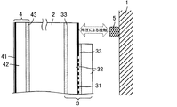
従来のPDPでは、ガラスからなる保護板の両面に、シールドフィルムと反射防止膜及び/又はアンチグレア膜とを貼合し、これをパネル本体の表面に装着していた。
図1に従来のPDPの一例の模式図を示した。
以下に本発明を詳述する。
これに対して本発明者らは、更に鋭意検討の結果、導電性メッシュ層とプラズマディスプレイパネル本体とを導電接続材により導電接続することによりこの課題を解決した。
上記金属からなる導電性テープ及び非金属性導電性テープにおいては、導電性テープの片面に粘着層を用いることができる。これは、ガラスからなる保護板に導電性テープを固定するとともに、粘着層の緩衝性により導電性面とパネル本体とを確実に接触させることができるためである。なお、上記粘着層の緩衝性が強い場合は、導電性スポンジを不要とできる。
上記導電性テープの粘着層の厚みとしては特に限定されないが、好ましい下限は10μm、好ましい上限は50μmである。
上記導電性を持った粘着層の厚みとしては特に限定されないが、好ましい下限は10μm、好ましい上限は100μmである。
本発明のプラズマディスプレイ装置の一実施態様の模式図を図3に示した。
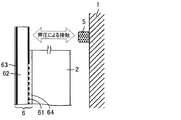
図3のPDPでは、パネル本体1の前面に、片面にフィルタ6が貼着されたガラスからなる保護板2が装着されている。フィルタ6は、基材62の一方の面に導電性メッシュ61が、他方の面に反射防止膜/アンチグレア膜63が形成された構造を有し、粘着層64を介して導電性メッシュ61側が保護板2に貼着されている。導電性メッシュ61とパネル本体1とは導電接続材7を介して導電接続されている。導電接続材7は、保護板2の側面に沿って配置され、保護板の両面に内側に織り込まれている。このような導電接続材7を用いることにより、フィルタ6側ではそのまま導電性メッシュ61が導電接続材7に接触し、パネル本体1側では従来の導電性スポンジ5を介して容易に導電接続材7がパネル本体1に導電接続される。
図4のPDPは、導電接続材7を用いた導電接続方法以外は図3のPDPと同一である。
導電接続材7は、保護板2の側面に沿って配置され、フィルタ6側では外側に、パネル本体1側では内側に織り込まれている。フィルタ6はごくわずかに保護板2からはみ出しており、そのはみ出し部分において導電性メッシュ61が導電接続材7に接触している。このはみ出し部分の長さや形状は、輸送時やパネル本体装着時に支障がないように適宜選定される。パネル本体1側の導電接続は、図3のPDPと同様である。
2 ガラスからなる保護板
3 シールドフィルム
31 導電性メッシュ
32 基材
33 粘着層
4 反射防止/アンチグレアフィルム
41 反射防止膜/アンチグレア膜
42 基材
43 粘着層
5 導電性スポンジ
6 フィルタ
61 導電性メッシュ
62 基材
63 反射防止膜/アンチグレア膜
64 粘着層
7 導電接続材
Claims (2)
- プラズマディスプレイパネル本体の前面に、ガラスからなる保護板、並びに、基材の一方の面に導電性メッシュを有し、かつ、他方の面に反射防止層及び/又はアンチグレア層を有するフィルタがこの順に装着された構造を有するプラズマディスプレイ装置であって、
前記フィルタの導電性メッシュ側が前記保護板に接着されており、
導電接続材が、前記保護板の側面に沿って配置され、導電性スポンジを介して前記導電接続材と前記プラズマディスプレイパネル本体とが導電接続されることで、
前記導電性メッシュ層と前記プラズマディスプレイパネル本体とが導電接続材及び導電性スポンジにより導電接続されていることを特徴とするプラズマディスプレイ装置。 - 導電接続材は、保護板の両面においてフィルタの導電性メッシュ及びプラズマディスプレイパネル本体と接触する形状を有することを特徴とする請求項1記載のプラズマディスプレイ装置。
Priority Applications (1)
| Application Number | Priority Date | Filing Date | Title |
|---|---|---|---|
| JP2007211893A JP5111012B2 (ja) | 2007-08-15 | 2007-08-15 | プラズマディスプレイ装置 |
Applications Claiming Priority (1)
| Application Number | Priority Date | Filing Date | Title |
|---|---|---|---|
| JP2007211893A JP5111012B2 (ja) | 2007-08-15 | 2007-08-15 | プラズマディスプレイ装置 |
Publications (2)
| Publication Number | Publication Date |
|---|---|
| JP2009047783A JP2009047783A (ja) | 2009-03-05 |
| JP5111012B2 true JP5111012B2 (ja) | 2012-12-26 |
Family
ID=40500097
Family Applications (1)
| Application Number | Title | Priority Date | Filing Date |
|---|---|---|---|
| JP2007211893A Expired - Fee Related JP5111012B2 (ja) | 2007-08-15 | 2007-08-15 | プラズマディスプレイ装置 |
Country Status (1)
| Country | Link |
|---|---|
| JP (1) | JP5111012B2 (ja) |
Family Cites Families (4)
| Publication number | Priority date | Publication date | Assignee | Title |
|---|---|---|---|---|
| KR100546261B1 (ko) * | 2003-07-22 | 2006-01-26 | 엘지전자 주식회사 | 표시 패널 모듈 |
| JP2007142334A (ja) * | 2005-11-22 | 2007-06-07 | Gunze Ltd | 電磁波シールド材及びその製造方法 |
| JP2008292745A (ja) * | 2007-05-24 | 2008-12-04 | Dainippon Printing Co Ltd | プラズマディスプレイ用前面ガラスフィルタ、及びその製造方法 |
| JP2009031720A (ja) * | 2007-06-28 | 2009-02-12 | Dainippon Printing Co Ltd | ディスプレイ用複合フィルタ |
-
2007
- 2007-08-15 JP JP2007211893A patent/JP5111012B2/ja not_active Expired - Fee Related
Also Published As
| Publication number | Publication date |
|---|---|
| JP2009047783A (ja) | 2009-03-05 |
Similar Documents
| Publication | Publication Date | Title |
|---|---|---|
| KR100540543B1 (ko) | 적층체 및 그것을 이용한 표시장치 | |
| US7214282B2 (en) | Electromagnetic-wave shielding and light transmitting plate, manufacturing method thereof and display panel | |
| KR100571810B1 (ko) | 플라즈마 디스플레이 패널용 전자파 차폐 필터와, 이의제조 방법 | |
| JP2005202410A (ja) | フィルター組立体及びその製造方法、並びにそれを採用したプラズマディスプレイパネル | |
| JP2003066854A (ja) | 光学フィルター及びプラズマディスプレイ装置 | |
| JPWO2010082514A1 (ja) | 電磁波シールド性前面フィルターのアース電極取り出し用導電性部材並びにそれを用いた構成体及びディスプレイ | |
| JP2003298284A (ja) | シールド材及びその製造方法 | |
| CN101248715B (zh) | 平面显示器部件及其制造方法以及平面显示器及其制造方法 | |
| JP2006098749A (ja) | ディスプレイ用フィルタ | |
| US7492081B2 (en) | Display panel module and method for manufacturing the same | |
| US20050077835A1 (en) | Thermal conductive medium for display device, method of fabricating the same, and plasma display panel assembly using the same | |
| JP2009047783A (ja) | プラズマディスプレイ装置 | |
| JP2010287590A (ja) | 電磁波遮蔽材及びそのアース取り出し構造 | |
| KR100746255B1 (ko) | 온 사이트형 pdp 전면 필터의 제조 방법 및 이에 의해제조된 전면 필터를 포함하는 플라즈마 디스플레이 패널 | |
| CN101006543B (zh) | Pdp滤光器以及使用完全蚀刻的电磁干扰膜制造该滤光器的方法 | |
| JP2003258488A (ja) | シールド材の製造方法 | |
| JP2007048789A (ja) | ディスプレイ用複合フィルタの製造方法 | |
| JP2006201794A (ja) | 平板表示装置用放熱シート及びそれを含んだ平板表示装置 | |
| JP2010278119A (ja) | 電磁波遮蔽材 | |
| JP2008292745A (ja) | プラズマディスプレイ用前面ガラスフィルタ、及びその製造方法 | |
| JP5293455B2 (ja) | 電磁波遮蔽材 | |
| WO2013046634A1 (ja) | 光学フィルタおよび表示装置 | |
| JP2003066852A (ja) | プラズマディスプレイ装置 | |
| KR100692096B1 (ko) | 플라즈마 디스플레이 패널용 전면 필터와 그의 제조 방법및 그를 구비한 플라즈마 디스플레이 장치 | |
| JP2008034590A (ja) | ディスプレイ用部材及びディスプレイ用部材の製造方法、ディスプレイ及びディスプレイの製造方法 |
Legal Events
| Date | Code | Title | Description |
|---|---|---|---|
| A621 | Written request for application examination |
Free format text: JAPANESE INTERMEDIATE CODE: A621 Effective date: 20100715 |
|
| RD02 | Notification of acceptance of power of attorney |
Free format text: JAPANESE INTERMEDIATE CODE: A7422 Effective date: 20100715 |
|
| A131 | Notification of reasons for refusal |
Free format text: JAPANESE INTERMEDIATE CODE: A131 Effective date: 20120207 |
|
| A977 | Report on retrieval |
Free format text: JAPANESE INTERMEDIATE CODE: A971007 Effective date: 20120208 |
|
| A521 | Written amendment |
Free format text: JAPANESE INTERMEDIATE CODE: A523 Effective date: 20120316 |
|
| TRDD | Decision of grant or rejection written | ||
| A01 | Written decision to grant a patent or to grant a registration (utility model) |
Free format text: JAPANESE INTERMEDIATE CODE: A01 Effective date: 20120911 |
|
| A01 | Written decision to grant a patent or to grant a registration (utility model) |
Free format text: JAPANESE INTERMEDIATE CODE: A01 |
|
| A61 | First payment of annual fees (during grant procedure) |
Free format text: JAPANESE INTERMEDIATE CODE: A61 Effective date: 20121009 |
|
| FPAY | Renewal fee payment (event date is renewal date of database) |
Free format text: PAYMENT UNTIL: 20151019 Year of fee payment: 3 |
|
| R150 | Certificate of patent or registration of utility model |
Free format text: JAPANESE INTERMEDIATE CODE: R150 |
|
| FPAY | Renewal fee payment (event date is renewal date of database) |
Free format text: PAYMENT UNTIL: 20151019 Year of fee payment: 3 |
|
| LAPS | Cancellation because of no payment of annual fees |