JP5113912B2 - プラズマディスプレイパネルおよびその製造方法 - Google Patents
プラズマディスプレイパネルおよびその製造方法 Download PDFInfo
- Publication number
- JP5113912B2 JP5113912B2 JP2010540234A JP2010540234A JP5113912B2 JP 5113912 B2 JP5113912 B2 JP 5113912B2 JP 2010540234 A JP2010540234 A JP 2010540234A JP 2010540234 A JP2010540234 A JP 2010540234A JP 5113912 B2 JP5113912 B2 JP 5113912B2
- Authority
- JP
- Japan
- Prior art keywords
- film
- electrode
- metal
- display panel
- discharge
- Prior art date
- Legal status (The legal status is an assumption and is not a legal conclusion. Google has not performed a legal analysis and makes no representation as to the accuracy of the status listed.)
- Expired - Fee Related
Links
Images

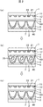


Classifications
-
- H—ELECTRICITY
- H01—ELECTRIC ELEMENTS
- H01J—ELECTRIC DISCHARGE TUBES OR DISCHARGE LAMPS
- H01J11/00—Gas-filled discharge tubes with alternating current induction of the discharge, e.g. alternating current plasma display panels [AC-PDP]; Gas-filled discharge tubes without any main electrode inside the vessel; Gas-filled discharge tubes with at least one main electrode outside the vessel
- H01J11/20—Constructional details
- H01J11/34—Vessels, containers or parts thereof, e.g. substrates
- H01J11/40—Layers for protecting or enhancing the electron emission, e.g. MgO layers
-
- H—ELECTRICITY
- H01—ELECTRIC ELEMENTS
- H01J—ELECTRIC DISCHARGE TUBES OR DISCHARGE LAMPS
- H01J11/00—Gas-filled discharge tubes with alternating current induction of the discharge, e.g. alternating current plasma display panels [AC-PDP]; Gas-filled discharge tubes without any main electrode inside the vessel; Gas-filled discharge tubes with at least one main electrode outside the vessel
- H01J11/10—AC-PDPs with at least one main electrode being out of contact with the plasma
- H01J11/12—AC-PDPs with at least one main electrode being out of contact with the plasma with main electrodes provided on both sides of the discharge space
-
- H—ELECTRICITY
- H01—ELECTRIC ELEMENTS
- H01J—ELECTRIC DISCHARGE TUBES OR DISCHARGE LAMPS
- H01J11/00—Gas-filled discharge tubes with alternating current induction of the discharge, e.g. alternating current plasma display panels [AC-PDP]; Gas-filled discharge tubes without any main electrode inside the vessel; Gas-filled discharge tubes with at least one main electrode outside the vessel
- H01J11/20—Constructional details
- H01J11/34—Vessels, containers or parts thereof, e.g. substrates
- H01J11/38—Dielectric or insulating layers
-
- H—ELECTRICITY
- H01—ELECTRIC ELEMENTS
- H01J—ELECTRIC DISCHARGE TUBES OR DISCHARGE LAMPS
- H01J9/00—Apparatus or processes specially adapted for the manufacture, installation, removal, maintenance of electric discharge tubes, discharge lamps, or parts thereof; Recovery of material from discharge tubes or lamps
- H01J9/02—Manufacture of electrodes or electrode systems
Landscapes
- Engineering & Computer Science (AREA)
- Physics & Mathematics (AREA)
- Plasma & Fusion (AREA)
- Manufacturing & Machinery (AREA)
- Gas-Filled Discharge Tubes (AREA)
- Manufacture Of Electron Tubes, Discharge Lamp Vessels, Lead-In Wires, And The Like (AREA)
Description
Claims (6)
- 第1の放電電極と第2の放電電極を覆って誘電体層が形成され、前記誘電体層を覆って保護膜が形成された前面基板と、アドレス電極を覆って誘電体層が形成され、前記誘電体層の上に隔壁が形成された背面基板とが、周辺に形成されたシール材によってシールされたプラズマディスプレイパネルであって、
前記保護膜の上には、SiO2、Al2O3、TiO2、MgO、ZrOのいずれかの金属酸化物と、Tb、La、Ce、Eu,Yb、Y、Scの希土類金属のいずれか、あるいは、Mg,Ca、Sr、Baのアルカリ土類金属のいずれか、あるいは、K、Naのアルカリ金属のいずれかの金属とによって構成され、かつ、膜厚が10nm〜500nmの不活性膜が形成され、
前記不活性膜は、プラズマ放電に曝される部分においては全部または一部が除去されていることを特徴とするプラズマディスプレイパネル。 - 前記金属酸化物の量をxとし、前記金属の量をyとした場合、y/(x+y)は0.5mol%〜50mol%であることを特徴とする請求項1に記載のプラズマディスプレイパネル。
- 前記保護膜は、SrO、CaO、BaOのいずれか、あるいは、これらのいずれかを含む混合物であることを特徴とする請求項1に記載のプラズマディスプレイパネル。
- 第1の放電電極と第2の放電電極を覆って誘電体層が形成され、前記誘電体層を覆って保護膜が形成され、前記保護膜の上に不活性膜が形成された前面基板と、アドレス電極を覆って誘電体層が形成され、前記誘電体層の上に隔壁が形成された背面基板とが、周辺に形成されたシール材によってシールされたプラズマディスプレイパネルの製造方法であって、
前記不活性膜は、SiO2、Al2O3、TiO2、MgO、ZrOのいずれかの金属酸化物と、Tb、La、Ce、Eu,Yb、Y、Scの希土類金属のいずれか、あるいは、Mg,Ca、Sr、Baのアルカリ土類金属のいずれか、あるいは、K、Naのアルカリ金属のいずれかの金属を、膜厚が10nm〜500nmとなるように蒸着によって同時成膜し、
前記不活性膜はエージング工程において、プラズマ放電に曝される部分の全部または一部において除去されることを特徴とするプラズマディスプレイパネルの製造方法。 - 前記蒸着は前記金属酸化物と前記金属を同一のハースに載置した蒸着材料を電子ビーム加熱によって加熱することを特徴とする請求項4に記載のプラズマディスプレイパネルの製造方法。
- 前記蒸着は前記金属酸化物と前記金属を別々のハースに載置し、前記金属酸化物と前記金属を別々に加熱、制御することによって行われることを特徴とする請求項4に記載のプラズマディスプレイパネルの製造方法。
Applications Claiming Priority (1)
| Application Number | Priority Date | Filing Date | Title |
|---|---|---|---|
| PCT/JP2008/003524 WO2010061425A1 (ja) | 2008-11-28 | 2008-11-28 | プラズマディスプレイパネルおよびその製造方法 |
Publications (2)
| Publication Number | Publication Date |
|---|---|
| JPWO2010061425A1 JPWO2010061425A1 (ja) | 2012-04-19 |
| JP5113912B2 true JP5113912B2 (ja) | 2013-01-09 |
Family
ID=42225319
Family Applications (1)
| Application Number | Title | Priority Date | Filing Date |
|---|---|---|---|
| JP2010540234A Expired - Fee Related JP5113912B2 (ja) | 2008-11-28 | 2008-11-28 | プラズマディスプレイパネルおよびその製造方法 |
Country Status (3)
| Country | Link |
|---|---|
| US (1) | US8692463B2 (ja) |
| JP (1) | JP5113912B2 (ja) |
| WO (1) | WO2010061425A1 (ja) |
Families Citing this family (1)
| Publication number | Priority date | Publication date | Assignee | Title |
|---|---|---|---|---|
| WO2012124284A1 (ja) * | 2011-03-15 | 2012-09-20 | パナソニック株式会社 | プラズマディスプレイパネル |
Citations (3)
| Publication number | Priority date | Publication date | Assignee | Title |
|---|---|---|---|---|
| JPH10149767A (ja) * | 1996-11-20 | 1998-06-02 | Fujitsu Ltd | プラズマディスプレイパネルの製造方法 |
| JP2000348626A (ja) * | 1999-06-01 | 2000-12-15 | Hitachi Ltd | プラズマディスプレイパネル、それを用いた表示装置及びその製造方法並びに製造装置 |
| JP2008091247A (ja) * | 2006-10-03 | 2008-04-17 | Matsushita Electric Ind Co Ltd | プラズマディスプレイパネル |
Family Cites Families (10)
| Publication number | Priority date | Publication date | Assignee | Title |
|---|---|---|---|---|
| JP2649276B2 (ja) | 1989-08-11 | 1997-09-03 | アルプス電気株式会社 | モード検出装置 |
| JP3563994B2 (ja) | 1999-04-12 | 2004-09-08 | 大日本印刷株式会社 | プラズマディスプレイパネル用前面板ユニットおよびそれを用いたプラズマディスプレイパネル |
| US7378796B2 (en) * | 2003-06-05 | 2008-05-27 | Matsushita Electric Industrial Co., Ltd. | Plasma display panel |
| WO2005098889A1 (ja) * | 2004-04-08 | 2005-10-20 | Matsushita Electric Industrial Co., Ltd. | ガス放電表示パネル |
| EP1808881B1 (en) * | 2004-11-05 | 2012-09-26 | Ulvac, Inc. | Plasma display panel-use protection film and production method for the protection film, plasma display panel and production method therefor |
| KR20070048017A (ko) * | 2005-11-03 | 2007-05-08 | 엘지전자 주식회사 | 플라즈마 디스플레이 패널의 보호막 |
| KR100765513B1 (ko) * | 2006-01-26 | 2007-10-10 | 엘지전자 주식회사 | 플라즈마 디스플레이 패널 및 그의 제조 방법 |
| JP4875976B2 (ja) * | 2006-12-27 | 2012-02-15 | パナソニック株式会社 | プラズマディスプレイパネル |
| JP2009170192A (ja) * | 2008-01-15 | 2009-07-30 | Panasonic Corp | プラズマディスプレイパネル |
| US8049423B2 (en) * | 2008-07-25 | 2011-11-01 | Samsung Sdi Co., Ltd. | Plasma display panel with improved luminance and low power consumption |
-
2008
- 2008-11-28 US US12/863,640 patent/US8692463B2/en not_active Expired - Fee Related
- 2008-11-28 WO PCT/JP2008/003524 patent/WO2010061425A1/ja not_active Ceased
- 2008-11-28 JP JP2010540234A patent/JP5113912B2/ja not_active Expired - Fee Related
Patent Citations (3)
| Publication number | Priority date | Publication date | Assignee | Title |
|---|---|---|---|---|
| JPH10149767A (ja) * | 1996-11-20 | 1998-06-02 | Fujitsu Ltd | プラズマディスプレイパネルの製造方法 |
| JP2000348626A (ja) * | 1999-06-01 | 2000-12-15 | Hitachi Ltd | プラズマディスプレイパネル、それを用いた表示装置及びその製造方法並びに製造装置 |
| JP2008091247A (ja) * | 2006-10-03 | 2008-04-17 | Matsushita Electric Ind Co Ltd | プラズマディスプレイパネル |
Also Published As
| Publication number | Publication date |
|---|---|
| US8692463B2 (en) | 2014-04-08 |
| JPWO2010061425A1 (ja) | 2012-04-19 |
| US20100289726A1 (en) | 2010-11-18 |
| WO2010061425A1 (ja) | 2010-06-03 |
Similar Documents
| Publication | Publication Date | Title |
|---|---|---|
| JPWO2007126061A1 (ja) | プラズマディスプレイパネルとその製造方法 | |
| US8004190B2 (en) | Plasma display panel and method for manufacture of the same | |
| JP4659118B2 (ja) | プラズマディスプレイパネルとその製造方法 | |
| KR100756153B1 (ko) | 플라즈마 디스플레이 패널 | |
| CN100372042C (zh) | 等离子体显示屏及其制造方法 | |
| US20080157672A1 (en) | Plasma display panel and manufacturing method therefor | |
| JP4543852B2 (ja) | プラズマディスプレイパネル | |
| US8222814B2 (en) | Plasma display panel with exposed crystal particles and manufacturing method thereof | |
| JP2004119118A (ja) | プラズマ表示装置およびその製造方法 | |
| JP5113912B2 (ja) | プラズマディスプレイパネルおよびその製造方法 | |
| US20080160346A1 (en) | Plasma display panel and manufacturing method therefor | |
| JP4100187B2 (ja) | プラズマディスプレイパネル | |
| JP2011181413A (ja) | 保護膜、保護膜の製造方法、プラズマディスプレイパネルおよびプラズマディスプレイパネルの製造方法 | |
| JP2008300127A (ja) | プラズマディスプレイパネル | |
| WO2011118152A1 (ja) | プラズマディスプレイパネルの製造方法 | |
| JP4102073B2 (ja) | プラズマディスプレイパネルおよびその製造方法 | |
| JP4360926B2 (ja) | プラズマディスプレイパネル | |
| JP2009217940A (ja) | プラズマディスプレイ装置 | |
| US20040038615A1 (en) | Production method for plasma display panel unit-use panel and production method for plasma display unit | |
| KR20020096015A (ko) | 플라즈마 표시 장치 및 그 제조 방법 | |
| JP2007323922A (ja) | プラズマディスプレイパネル | |
| JP2009283351A (ja) | 保護膜、保護膜の製造方法、プラズマディスプレイパネル及びプラズマディスプレイパネルの製造方法 | |
| JP2007026794A (ja) | 保護層用原材料 | |
| JP2007042654A (ja) | プラズマディスプレイパネル | |
| JP2004265656A (ja) | プラズマディスプレイパネルおよびその製造方法 |
Legal Events
| Date | Code | Title | Description |
|---|---|---|---|
| A131 | Notification of reasons for refusal |
Free format text: JAPANESE INTERMEDIATE CODE: A131 Effective date: 20120124 |
|
| A521 | Request for written amendment filed |
Free format text: JAPANESE INTERMEDIATE CODE: A523 Effective date: 20120308 |
|
| A711 | Notification of change in applicant |
Free format text: JAPANESE INTERMEDIATE CODE: A711 Effective date: 20120319 |
|
| A131 | Notification of reasons for refusal |
Free format text: JAPANESE INTERMEDIATE CODE: A131 Effective date: 20120424 |
|
| A521 | Request for written amendment filed |
Free format text: JAPANESE INTERMEDIATE CODE: A523 Effective date: 20120611 |
|
| TRDD | Decision of grant or rejection written | ||
| A01 | Written decision to grant a patent or to grant a registration (utility model) |
Free format text: JAPANESE INTERMEDIATE CODE: A01 Effective date: 20120918 |
|
| A01 | Written decision to grant a patent or to grant a registration (utility model) |
Free format text: JAPANESE INTERMEDIATE CODE: A01 |
|
| A61 | First payment of annual fees (during grant procedure) |
Free format text: JAPANESE INTERMEDIATE CODE: A61 Effective date: 20121012 |
|
| FPAY | Renewal fee payment (event date is renewal date of database) |
Free format text: PAYMENT UNTIL: 20151019 Year of fee payment: 3 |
|
| R150 | Certificate of patent or registration of utility model |
Free format text: JAPANESE INTERMEDIATE CODE: R150 |
|
| S111 | Request for change of ownership or part of ownership |
Free format text: JAPANESE INTERMEDIATE CODE: R313111 |
|
| R350 | Written notification of registration of transfer |
Free format text: JAPANESE INTERMEDIATE CODE: R350 |
|
| S111 | Request for change of ownership or part of ownership |
Free format text: JAPANESE INTERMEDIATE CODE: R313111 |
|
| R350 | Written notification of registration of transfer |
Free format text: JAPANESE INTERMEDIATE CODE: R350 |
|
| LAPS | Cancellation because of no payment of annual fees |