JP5114773B2 - Surface mount light emitting device - Google Patents
Surface mount light emitting device Download PDFInfo
- Publication number
- JP5114773B2 JP5114773B2 JP2007209973A JP2007209973A JP5114773B2 JP 5114773 B2 JP5114773 B2 JP 5114773B2 JP 2007209973 A JP2007209973 A JP 2007209973A JP 2007209973 A JP2007209973 A JP 2007209973A JP 5114773 B2 JP5114773 B2 JP 5114773B2
- Authority
- JP
- Japan
- Prior art keywords
- light emitting
- peeling
- light
- interface
- emitting element
- Prior art date
- Legal status (The legal status is an assumption and is not a legal conclusion. Google has not performed a legal analysis and makes no representation as to the accuracy of the status listed.)
- Expired - Fee Related
Links
Images


Classifications
-
- H—ELECTRICITY
- H10—SEMICONDUCTOR DEVICES; ELECTRIC SOLID-STATE DEVICES NOT OTHERWISE PROVIDED FOR
- H10H—INORGANIC LIGHT-EMITTING SEMICONDUCTOR DEVICES HAVING POTENTIAL BARRIERS
- H10H20/00—Individual inorganic light-emitting semiconductor devices having potential barriers, e.g. light-emitting diodes [LED]
- H10H20/80—Constructional details
- H10H20/85—Packages
- H10H20/857—Interconnections, e.g. lead-frames, bond wires or solder balls
-
- H—ELECTRICITY
- H10—SEMICONDUCTOR DEVICES; ELECTRIC SOLID-STATE DEVICES NOT OTHERWISE PROVIDED FOR
- H10H—INORGANIC LIGHT-EMITTING SEMICONDUCTOR DEVICES HAVING POTENTIAL BARRIERS
- H10H20/00—Individual inorganic light-emitting semiconductor devices having potential barriers, e.g. light-emitting diodes [LED]
- H10H20/80—Constructional details
- H10H20/85—Packages
- H10H20/852—Encapsulations
-
- H—ELECTRICITY
- H10—SEMICONDUCTOR DEVICES; ELECTRIC SOLID-STATE DEVICES NOT OTHERWISE PROVIDED FOR
- H10W—GENERIC PACKAGES, INTERCONNECTIONS, CONNECTORS OR OTHER CONSTRUCTIONAL DETAILS OF DEVICES COVERED BY CLASS H10
- H10W90/00—Package configurations
- H10W90/701—Package configurations characterised by the relative positions of pads or connectors relative to package parts
- H10W90/751—Package configurations characterised by the relative positions of pads or connectors relative to package parts of bond wires
- H10W90/754—Package configurations characterised by the relative positions of pads or connectors relative to package parts of bond wires between a chip and a stacked insulating package substrate, interposer or RDL
Landscapes
- Led Device Packages (AREA)
Description
本発明は、表面実装型発光装置に関し、特に、基板上に配置したLEDチップを樹脂によって封止した表面実装型LEDに関する。 The present invention relates to a surface-mounted light emitting device, and more particularly to a surface-mounted LED in which an LED chip disposed on a substrate is sealed with a resin.
表面実装型LEDは、例えば特許文献1に記載されているように、基板の上面から側面を経て裏面に回り込むように一対の回路パターンが形成され、基板の上面にLEDチップが搭載されている。LEDチップの底面電極は、一対の回路パターンに導電性接着剤等により電気的に接続され、上面電極は、他方の回路パターンとワイヤボンディング等により電気的に接続される。LEDチップは、ワイヤボンディングや回路パターンの一部と共に、発光波長に対して透明な樹脂により埋め込まれ、封止される。 For example, as described in Patent Document 1, a surface-mounted LED has a pair of circuit patterns formed so as to wrap around from the upper surface of the substrate to the back surface through the side surface, and the LED chip is mounted on the upper surface of the substrate. The bottom electrode of the LED chip is electrically connected to a pair of circuit patterns by a conductive adhesive or the like, and the top electrode is electrically connected to the other circuit pattern by wire bonding or the like. The LED chip is embedded and sealed with a resin transparent to the emission wavelength together with a part of the wire bonding and the circuit pattern.
このような表面実装型LEDは、他の電子部品等と共に、実装基板上に実装することができる。実装には、はんだリフロー法が一般的に用いられる。はんだリフロー時には、全体が高温に加熱されるため、表面実装型LEDの封止樹脂の熱膨張係数と、回路パターン11の熱膨張係数との差によって、回路パターン11と封止樹脂との界面に熱応力が生じる。この熱応力により、LEDチップを回路パターンの上方に持ち上げる力が働き、LEDチップと回路パターンとが剥離し、電気的導通を不良にすることがある。
Such a surface-mounted LED can be mounted on a mounting substrate together with other electronic components. A solder reflow method is generally used for mounting. At the time of solder reflow, since the whole is heated to a high temperature, the interface between the
これを防ぐために、特許文献1に記載の技術では、LEDチップの下に、回路パターンが形成されていない部分を設け、基板を構成する絶縁物が露出されるようにしている。LEDチップは回路パターンに搭載されるため、露出した絶縁物とLEDチップの底面との間には回路パターンの高さ分の間隙が生じ、この間隙に封止樹脂が回りこみ、基板と封止樹脂とが密着する。樹脂と絶縁物(基板)との密着力は、樹脂と金属(回路パターン)との密着力よりも強いため、はんだリフロー時の加熱により封止樹脂と回路パターンとの間に熱応力が加わっても、LEDチップと回路パターンとの剥離を防止することができる。 In order to prevent this, in the technique described in Patent Document 1, a portion where a circuit pattern is not formed is provided under the LED chip so that an insulator constituting the substrate is exposed. Since the LED chip is mounted on the circuit pattern, a gap corresponding to the height of the circuit pattern is generated between the exposed insulator and the bottom surface of the LED chip. The resin comes into close contact. Since the adhesion between the resin and the insulator (substrate) is stronger than the adhesion between the resin and the metal (circuit pattern), thermal stress is applied between the sealing resin and the circuit pattern due to heating during solder reflow. In addition, peeling between the LED chip and the circuit pattern can be prevented.
特許文献1に記載の技術は、LEDチップと基板との密着性を向上させる技術であるが、はんだリフロー時に生じる熱応力は、封止樹脂とLEDチップとの界面においても生じている。このため、封止樹脂がLEDチップとの界面から剥がれる界面剥離を生じる。 The technique described in Patent Document 1 is a technique for improving the adhesion between the LED chip and the substrate, but thermal stress generated during solder reflow is also generated at the interface between the sealing resin and the LED chip. For this reason, interface peeling which peels the sealing resin from the interface with the LED chip occurs.
封止樹脂とLEDチップとの界面で剥離が生じると、剥離部分に微小な空間が生じ、LEDチップから発光された輝度低下の原因となる。通常LEDチップは直方体形状であるため、周囲の樹脂との界面の応力は角の部分に集中し、角の部分から剥離しやすい。一旦剥離が生じると、その部分の接着力が弱まるため、応力が剥離箇所で放出されやすくなり、剥離の面積が広がっていく。 When peeling occurs at the interface between the sealing resin and the LED chip, a minute space is formed in the peeling portion, which causes a decrease in luminance emitted from the LED chip. Usually, since the LED chip has a rectangular parallelepiped shape, the stress at the interface with the surrounding resin is concentrated on the corner portion and easily peeled off from the corner portion. Once delamination occurs, the adhesive strength of the portion is weakened, so that stress is easily released at the delamination site, and the area of delamination increases.
本発明の目的は、LEDチップ表面での剥離を防止することのできる表面実装型LEDを提供することにある。 An object of the present invention is to provide a surface-mounted LED that can prevent peeling on the surface of an LED chip.
上記目的を達成するために、本発明によれば、以下のような表面実装型発光装置が提供される。すなわち、第1の態様の表面実装型発光装置は、基板と、基板上に配置された一対の回路パターンと、発光素子とを有し、一対の回路パターンのうち一方は、発光素子を搭載する素子搭載領域を備え、他方は、発光素子にワイヤにより接続されるワイヤ接続領域を備えている。一対の回路パターンには、素子搭載領域およびワイヤ接続領域よりも厚い、厚膜部が設けられている。これにより、装置を加熱した場合に、厚膜部と封止樹脂との界面において、発光素子と封止樹脂との界面よりも早く界面剥離を生じさせることが可能であり、これにより封止樹脂の応力を放出させ、発光素子と封止樹脂との界面剥離を防止できる。 In order to achieve the above object, according to the present invention, the following surface mount type light emitting device is provided. That is, the surface-mount light-emitting device according to the first aspect includes a substrate, a pair of circuit patterns disposed on the substrate, and a light-emitting element, and one of the pair of circuit patterns mounts the light-emitting element. An element mounting area is provided, and the other is provided with a wire connection area connected to the light emitting element by a wire. The pair of circuit patterns are provided with thick film portions that are thicker than the element mounting region and the wire connection region. As a result, when the apparatus is heated, it is possible to cause interface peeling at the interface between the thick film portion and the sealing resin faster than the interface between the light emitting element and the sealing resin. Can be released, and the interface peeling between the light emitting element and the sealing resin can be prevented.
上述厚膜部の外形は、角部を有することが好ましい。これにより、厚膜部の角部に熱膨張応力が集中するため、封止樹脂の剥離がより生じやすくなり、発光素子と樹脂との界面での剥離を防止できる。 The outer shape of the thick film portion preferably has a corner portion. Thereby, since thermal expansion stress concentrates on the corners of the thick film portion, the sealing resin is more easily peeled off, and peeling at the interface between the light emitting element and the resin can be prevented.
厚膜部は、例えば、素子搭載領域およびワイヤ接続領域のうち、厚い方の膜厚の2倍以上の厚さに設定することが望ましい。また、例えば、厚膜部の厚さを、例えば発光素子の高さ以上の厚さに設定することが望ましい。 For example, it is desirable that the thick film portion is set to have a thickness that is twice or more of the thicker one of the element mounting region and the wire connection region. Further, for example, it is desirable to set the thickness of the thick film portion to a thickness equal to or higher than the height of the light emitting element, for example.
また、第2の態様の表面実装型発光装置は、基板と、基板上に配置された一対の回路パターンと、発光素子とを有し、一方の回路パターンは、発光素子を搭載する素子搭載領域を備え、他方の回路パターンは、発光素子にワイヤにより接続されるワイヤ接続領域を備えている。基板上には、発光素子と樹脂との界面よりも先に界面剥離を引き起こすための剥離誘起構造体が配置されている。剥離誘起構造体は、発光素子よりも高さの大きい半導体製物体である。これにより、装置を加熱した場合に、半導体製物体と封止樹脂との界面において、発光素子と封止樹脂との界面よりも早く、界面剥離を生じさせることが可能であり、発光素子と封止樹脂との界面剥離を防止できる。 The surface-mount light-emitting device according to the second aspect includes a substrate, a pair of circuit patterns disposed on the substrate, and a light-emitting element, and one circuit pattern is an element mounting region on which the light-emitting element is mounted. The other circuit pattern includes a wire connection region connected to the light emitting element by a wire. On the substrate, a peeling inducing structure for causing interface peeling is arranged before the interface between the light emitting element and the resin. The exfoliation inducing structure is a semiconductor object having a height higher than that of the light emitting element. As a result, when the apparatus is heated, it is possible to cause interface peeling at the interface between the semiconductor object and the sealing resin faster than the interface between the light emitting element and the sealing resin. Interfacial peeling with the stop resin can be prevented.
本発明によれば、はんだリフロー時に発光装置を加熱した場合に、発光素子と封止樹脂との界面で剥離が生じるよりも早いタイミングで、厚膜部と封止樹脂との界面において界面剥離を生じさせることが可能であり、発光素子と封止樹脂との界面剥離を防止できる。これにより、発光素子の輝度低下を防止できる。 According to the present invention, when the light emitting device is heated during solder reflow, the interface peeling is performed at the interface between the thick film portion and the sealing resin at a timing earlier than the peeling occurs at the interface between the light emitting element and the sealing resin. It is possible to prevent the interface peeling between the light emitting element and the sealing resin. Thereby, the brightness | luminance fall of a light emitting element can be prevented.
本発明の一実施の形態の表面実装型LEDについて図面を用いて説明する。
(第1の実施の形態)
本実施の形態の表面実装型LEDの構造を図1を用いて説明する。(ただし、図1では、封止樹脂16内部に配置された物の形状を明確に示すため、樹脂16内の物の外形を実線で描いている。)図1のように、表面実装型LEDは、基板10と、基板10の上面に配置された一対の回路パターン11,12と、LEDチップ13とを有している。回路パターン12は、基板10の上面にチップ搭載領域22を備え、LEDチップ13は、この領域に搭載されている。回路パターン11は、基板10の上面に、ボンディング領域21と、他の部分よりも厚く形成された厚膜金属層部15とを備えている。厚膜金属層部15の詳しい構成および作用については後述する。回路パターン11、12はそれぞれ、基板10の上面のみならず、側面を通って裏面に回り込むように形成され、基板10の裏面側から給電可能な構成になっている。
A surface-mounted LED according to an embodiment of the present invention will be described with reference to the drawings.
(First embodiment)
The structure of the surface-mounted LED of this embodiment will be described with reference to FIG. (However, in FIG. 1, in order to clearly show the shape of the object disposed inside the
LEDチップ13は、直方体形状であり、図示していないが下面電極および上面電極を備えている。下面電極は、導電性接着剤により回路パターン12のチップ搭載領域22に接着され、これにより電気的に接続されている。上面電極には、ボンディングワイヤ14の一端がボンディング接続されている。ボンディングワイヤ14の他端は、回路パターン11のボンディング領域22に接続されている。
The
基板10の上面は、封止樹脂16によって封止されている。封止樹脂16は、LEDチップ13、ボンディングワイヤ14、回路パターン11のボンディング領域21、および、回路パターン12のチップ搭載領域22を覆っている。封止樹脂16の材質は、LEDチップ13の発光する光に対して透明なものであって、はんだリフロー時の加熱(一例として250℃程度)に耐えられるものを用いる。封止樹脂16としては、具体的には熱硬化樹脂、光硬化性樹脂や低融点ガラスなどを用いることができる。特にエポキシ樹脂、シリコーン樹脂、エポキシ基を有するポリジメチルシロキサン誘導体、オキセタン樹脂、アクリル樹脂、シクロオレフィン樹脂等の熱硬化樹脂が好ましい。これら樹脂は、1種または2種以上を混合して用いることができる。
The upper surface of the
回路パターン11、12は、LEDの回路パターンに一般的に用いられる金属材料によって形成することができ、単層構造であっても多層構造であってもよい。
The
本実施の形態では、LEDチップ13と封止樹脂16の熱膨張率の差により、はんだリフロー時にLEDチップ13と封止樹脂16との界面に剥離が生じるのを防止するため、LEDチップ13よりも先に界面剥離を生じる構造として、厚膜金属層部15を設けている。具体的には、図1のように、回路パターン11の一部の領域を、他の部分よりも厚く形成することにより厚膜金属層部15としている。厚膜金属層部15は、金属材料からなるため、LEDチップ13を構成する半導体材料よりも、封止樹脂16との熱膨張率の差が大きい。よって、加熱により厚膜金属層部15と封止樹脂15との界面に生じる歪みは、LEDチップ13において生じる歪みよりも大きくなり、図2に示すように、LEDチップ13より先に、厚膜金属層部15において界面剥離部25を生じさせることができる。(ただし、図2にておいも、封止樹脂16内部に配置された物の形状を明確に示すため、樹脂16内の物の外形を実線で描いている。)はんだリフロー時に、厚膜金属層部15においてLEDチップ13より先に界面剥離を生じた場合、封止樹脂16の熱膨張応力は当該界面剥離部25において放出され、LEDチップ13においては剥離が生じないか、生じたとしても光学特性(輝度等)に影響を与えない程度の軽微な剥離に抑制することができる。
In the present embodiment, in order to prevent peeling at the interface between the
厚膜金属層部15の位置は、封止樹脂16内のLEDチップ13から離れた位置、例えば封止樹脂16の辺縁部に配置することが望ましい。厚膜金属層部15と封止樹脂16との界面で界面剥離を生じさせるため、界面剥離部25の光学的な変化が、LEDチップ13から発せられた光に影響を与えないようにするためである。
The position of the thick
厚膜金属層部15の形状は、封止樹脂16との間に生じる膨張応力を大きくするため、封止樹脂16の膨張を妨げる高さ(厚さ)があることが望ましく、少なくとも、チップ搭載領域22の厚さおよびボンディング領域21のうちの厚い方の厚さよりも厚いことが望ましい。具体的には、後述のように、チップ搭載領域22の厚さおよびボンディング領域21のうちの厚い方の厚さの1.6倍以上が望ましく、2.0倍以上であることがさらに望ましい。LEDチップ13の高さ以上である場合には特に望ましい。
The thickness of the thick film
また、膨張応力を1点に集中させて剥離を生じやすくするために、厚膜金属層部15の形状は、直方体や立方体のように角部がある形状が好ましい。
Further, in order to concentrate the expansion stress at one point and easily cause peeling, the shape of the
厚膜金属層部15は、単層膜であっても多層膜であってもよく、回路パターン11の形成に一般に用いられる層構成および成膜方法により形成することができる。例えば、メッキ法により成膜することができる。多層膜構造とする場合、そのうちの1以上の層を厚膜金属層部15部分のみ厚く形成することにより、回路パターン11の他の部分と厚膜金属層部15とを同時に形成することができる。例えば、成膜時に他の部分をレジストで被覆することにより、厚膜金属層部15に他の部分より厚い膜を形成することができる。
The thick
ここで、厚膜金属層部15の厚さが、チップ搭載領域22の厚さおよびボンディング領域21の厚さよりもどれくらい厚ければ、LEDチップ13よりも先に界面剥離を生じさせることが可能であるかを調べるために以下の実験を行った。
Here, if the thickness of the thick
表面実装型LEDの構造は、図1の構造とした。回路パターン11、12は、最表面をAuとするAu/Ni/Cuの積層金属膜により形成した。封止樹脂16は、エポキシ樹脂を用いた。チップ搭載領域22の厚さを50μm、ボンディング領域21の厚さを50μmとした。厚膜金属層部15の膜厚が、チップ搭載領域22およびボンディング領域21の厚さ(50μm)の1.5倍(75μm)、1.6倍(80μm)、2倍(100μm)の3つの試料を用意し、同一の湿度環境にて封止樹脂16に一定量吸湿させた後に、所定温度(260℃)まで加熱し、LEDチップ13に剥離が生じるかどうかを観察した。その結果を表1に示す。
The structure of the surface-mounted LED is the structure shown in FIG. The
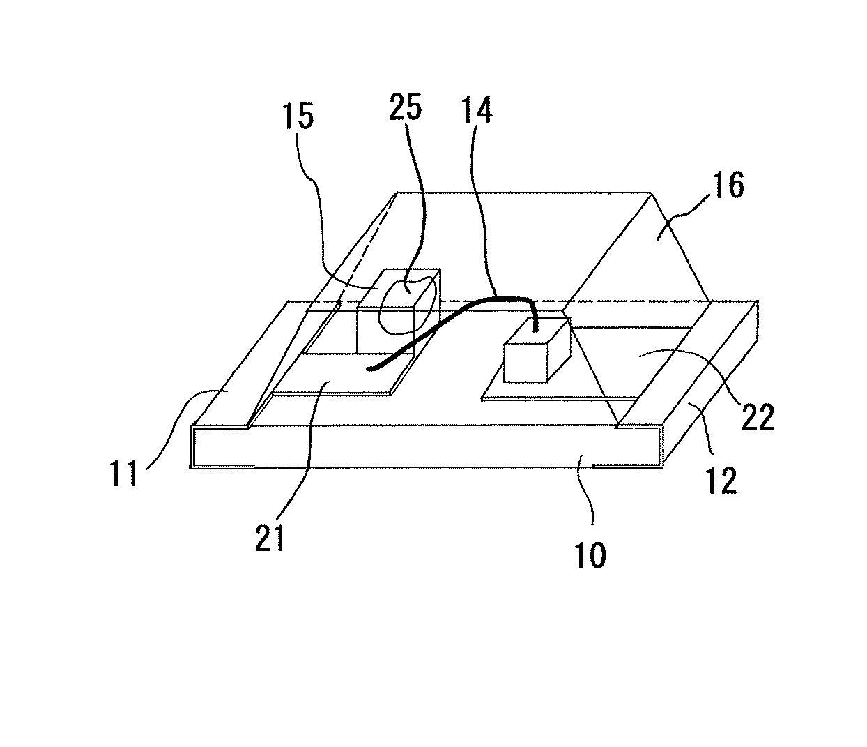
表1から明らかなように、厚膜金属層部15を配置し、その膜厚を厚くすることにより、LEDチップ13と封止樹脂16の界面の剥離を防止できることが確認できた。なお、表1において、試料1、2、3ともに、厚膜金属層部15と封止樹脂16の界面では、剥離が生じていた。
As can be seen from Table 1, it was confirmed that peeling of the interface between the
また、試料1、2、3において、LEDチップ13と封止樹脂16の界面に剥離が生じるまで徐々に温度を上げて、剥離開始温度を調べたところ、試料1(75μm)が最も低く、試料2(80μm)、試料3(100μm)の順に高温であった。これにより、厚膜金属層部15が厚いほど、剥離開始温度が高くなることが確認できた。
In Samples 1, 2, and 3, the temperature was gradually raised until peeling occurred at the interface between the
以上のことから、厚膜金属層部15の厚さが、チップ搭載領域22およびボンディング領域21の厚さの1.6倍以上である場合、LEDチップ13における界面剥離による輝度低下を防止でき、2倍以上である場合、LEDチップ13における界面剥離を防止でき、さらに望ましいことが確認された。
From the above, when the thickness of the thick film
上述のように、本実施の形態によれば、回路パターン11の一部を厚く形成した厚膜金属層部15を設けるという簡単な構成によって、はんだリフロー時のLEDチップ13と封止樹脂16との界面剥離を防止することができる。これにより、LEDの輝度低下を防止でき、高性能な表面実装型LEDを提供することができる。
As described above, according to the present embodiment, the
(第2の実施の形態)
第2の実施の形態の表面実装型LEDは、第1の実施の形態の厚膜金属層部15に代えて、LEDチップ13と封止樹脂16との界面よりも先に界面剥離を引き起こすための剥離誘起構造体として、半導体製のダミー構造物を搭載する。半導体製のダミー構造物の搭載位置は、厚膜金属層部15と同様である。ただし、半導体製のダミー構造物は、同じ半導体のLEDチップ13と熱膨張率が同程度であるため、その高さが、LEDチップ13よりも大きいものを用いる。また、半導体製ダミー構造物は、上面積と側面積の和が、LEDチップ13よりも大きいことが望ましい。
(Second Embodiment)
The surface-mounted LED according to the second embodiment causes interface peeling before the interface between the
このように、高さの大きい半導体製ダミー構造物は、封止樹脂16の膨張をLEDチップ13よりも妨げる作用が大きいため、同程度の熱膨張率であっても、先に界面剥離を生じる。これにより、ダミー構造物に生じた界面剥離部分において、封止樹脂16の膨張応力が緩和され、LEDチップ13における界面剥離を防止できる。
As described above, since the semiconductor dummy structure having a large height has a larger effect of preventing the expansion of the sealing
半導体製のダミー構造物としては、例えば、LEDチップを用いることができる。 As the semiconductor dummy structure, for example, an LED chip can be used.
10…基板、11、12…回路パターン、13…LEDチップ、14…ボンディングワイヤ、15…厚膜金属層部、16…封止樹脂、21…ボンディング領域、22…LED搭載領域、25…界面剥離。
DESCRIPTION OF
Claims (5)
前記一対の回路パターンのうち一方は、前記発光素子を搭載する素子搭載領域を備え、他方は、前記発光素子にワイヤにより接続されるワイヤ接続領域を備え、
前記基板上には、前記発光素子と樹脂との界面よりも先に界面剥離を引き起こすための剥離誘起構造体が配置され、
該剥離誘起構造体として、前記一対の回路パターンには、前記素子搭載領域および前記ワイヤ接続領域のうち厚い方の膜厚の1.6倍以上の厚さを有し、金属材料から成る厚膜部が設けられていることを特徴とする表面実装型発光装置。 A substrate, a pair of circuit patterns disposed on the substrate, a light emitting element, and a resin that seals the light emitting element;
One of the pair of circuit patterns includes an element mounting area for mounting the light emitting element, and the other includes a wire connection area connected to the light emitting element by a wire,
On the substrate, a peeling inducing structure for causing interface peeling before the interface between the light emitting element and the resin is disposed,
As the delamination-inducing structure, the pair of circuit patterns has a thickness of 1.6 times or more of the thicker one of the element mounting region and the wire connection region, and is a thick film made of a metal material A surface-mounted light emitting device characterized in that a portion is provided.
Priority Applications (2)
| Application Number | Priority Date | Filing Date | Title |
|---|---|---|---|
| JP2007209973A JP5114773B2 (en) | 2007-08-10 | 2007-08-10 | Surface mount light emitting device |
| US12/187,597 US7750361B2 (en) | 2007-08-10 | 2008-08-07 | Surface mount light emitting apparatus |
Applications Claiming Priority (1)
| Application Number | Priority Date | Filing Date | Title |
|---|---|---|---|
| JP2007209973A JP5114773B2 (en) | 2007-08-10 | 2007-08-10 | Surface mount light emitting device |
Publications (2)
| Publication Number | Publication Date |
|---|---|
| JP2009044082A JP2009044082A (en) | 2009-02-26 |
| JP5114773B2 true JP5114773B2 (en) | 2013-01-09 |
Family
ID=40430874
Family Applications (1)
| Application Number | Title | Priority Date | Filing Date |
|---|---|---|---|
| JP2007209973A Expired - Fee Related JP5114773B2 (en) | 2007-08-10 | 2007-08-10 | Surface mount light emitting device |
Country Status (2)
| Country | Link |
|---|---|
| US (1) | US7750361B2 (en) |
| JP (1) | JP5114773B2 (en) |
Families Citing this family (5)
| Publication number | Priority date | Publication date | Assignee | Title |
|---|---|---|---|---|
| USD609653S1 (en) | 2008-10-07 | 2010-02-09 | Kabushiki Kaisha Toshiba | Light receiving and emitting device |
| JP2014135471A (en) * | 2012-12-10 | 2014-07-24 | Nitto Denko Corp | Light emitting device, light emitting device assembly, and substrate with electrode |
| USD753612S1 (en) * | 2012-09-07 | 2016-04-12 | Cree, Inc. | Light emitter device |
| TWD161897S (en) * | 2013-02-08 | 2014-07-21 | 晶元光電股份有限公司 | Portion of light-emitting diode |
| USD847102S1 (en) | 2013-02-08 | 2019-04-30 | Epistar Corporation | Light emitting diode |
Family Cites Families (27)
| Publication number | Priority date | Publication date | Assignee | Title |
|---|---|---|---|---|
| JP3672280B2 (en) * | 1996-10-29 | 2005-07-20 | 株式会社シチズン電子 | Manufacturing method of electronic component with through-hole electrode |
| JP3673621B2 (en) * | 1997-07-30 | 2005-07-20 | ローム株式会社 | Chip light emitting device |
| JPH1146018A (en) * | 1997-07-28 | 1999-02-16 | Citizen Electron Co Ltd | Surface mount type light emitting diode |
| JP4174858B2 (en) * | 1998-07-06 | 2008-11-05 | 日亜化学工業株式会社 | Light emitting diode |
| JP2000124506A (en) * | 1998-10-15 | 2000-04-28 | Rohm Co Ltd | Semiconductor light emitting device |
| JP2000188425A (en) * | 1998-12-22 | 2000-07-04 | Nichia Chem Ind Ltd | Light emitting diode |
| JP2001036140A (en) * | 1999-07-16 | 2001-02-09 | Stanley Electric Co Ltd | Antistatic surface mount LED |
| JP2002124703A (en) * | 2000-08-09 | 2002-04-26 | Rohm Co Ltd | Chip type light emitting device |
| JP4097949B2 (en) * | 2001-04-20 | 2008-06-11 | シャープ株式会社 | Spatial optical transmission system |
| JP4045781B2 (en) * | 2001-08-28 | 2008-02-13 | 松下電工株式会社 | Light emitting device |
| JP4211359B2 (en) * | 2002-03-06 | 2009-01-21 | 日亜化学工業株式会社 | Manufacturing method of semiconductor device |
| JP4085899B2 (en) * | 2003-06-30 | 2008-05-14 | 日立エーアイシー株式会社 | LIGHT EMITTING DEVICE SUBSTRATE AND LIGHT EMITTING DEVICE |
| JP4282392B2 (en) * | 2003-07-11 | 2009-06-17 | 株式会社東芝 | Optical semiconductor device and manufacturing method thereof |
| JP4788109B2 (en) * | 2003-10-28 | 2011-10-05 | パナソニック電工株式会社 | Semiconductor light emitting device and manufacturing method thereof |
| JP2005197329A (en) * | 2004-01-05 | 2005-07-21 | Stanley Electric Co Ltd | Surface mount semiconductor device and lead frame structure thereof |
| JP2005347401A (en) * | 2004-06-01 | 2005-12-15 | Meiko:Kk | Optical element chip parts |
| JP4359195B2 (en) * | 2004-06-11 | 2009-11-04 | 株式会社東芝 | Semiconductor light emitting device, manufacturing method thereof, and semiconductor light emitting unit |
| JP2006093672A (en) * | 2004-08-26 | 2006-04-06 | Toshiba Corp | Semiconductor light emitting device |
| WO2006059828A1 (en) * | 2004-09-10 | 2006-06-08 | Seoul Semiconductor Co., Ltd. | Light emitting diode package having multiple molding resins |
| JP4626258B2 (en) * | 2004-10-18 | 2011-02-02 | 日亜化学工業株式会社 | Light emitting diode |
| JP2006190888A (en) * | 2005-01-07 | 2006-07-20 | Stanley Electric Co Ltd | Surface mount type LED |
| JP4711715B2 (en) * | 2005-03-30 | 2011-06-29 | 株式会社東芝 | Semiconductor light emitting device and semiconductor light emitting unit |
| TW200717866A (en) * | 2005-07-29 | 2007-05-01 | Toshiba Kk | Semiconductor light emitting device |
| JP4835104B2 (en) * | 2005-10-24 | 2011-12-14 | 日亜化学工業株式会社 | Semiconductor light emitting device |
| JP2007142044A (en) * | 2005-11-16 | 2007-06-07 | Stanley Electric Co Ltd | Semiconductor light emitting device and surface light source using the same |
| JP2007212915A (en) * | 2006-02-13 | 2007-08-23 | Seiko Epson Corp | Photoelectric composite substrate and electronic device |
| TWM302123U (en) * | 2006-06-13 | 2006-12-01 | Lighthouse Technology Co Ltd | The stand structure of light-emitting diode |
-
2007
- 2007-08-10 JP JP2007209973A patent/JP5114773B2/en not_active Expired - Fee Related
-
2008
- 2008-08-07 US US12/187,597 patent/US7750361B2/en not_active Expired - Fee Related
Also Published As
| Publication number | Publication date |
|---|---|
| JP2009044082A (en) | 2009-02-26 |
| US20090065796A1 (en) | 2009-03-12 |
| US7750361B2 (en) | 2010-07-06 |
Similar Documents
| Publication | Publication Date | Title |
|---|---|---|
| JP5340583B2 (en) | Semiconductor light emitting device | |
| KR101044200B1 (en) | Rigid-Flexible Circuit Boards and Manufacturing Method Thereof | |
| KR102332362B1 (en) | Ultra-thin embedded semiconductor device package and method of manufacturing therof | |
| JP4516320B2 (en) | LED board | |
| JPWO2007116544A1 (en) | Composite substrate and method for manufacturing composite substrate | |
| JP2020161697A (en) | Semiconductor light emitting device | |
| JPWO2007110985A1 (en) | Composite substrate and method for manufacturing composite substrate | |
| JP2009044082A (en) | Surface mount light emitting device | |
| JPWO2007132612A1 (en) | Composite substrate and manufacturing method thereof | |
| JP2015192095A (en) | Led light-emitting device and method of manufacturing led light-emitting device | |
| JP5691573B2 (en) | Manufacturing method of module parts | |
| CN103124468A (en) | Metal copper clad laminate and method of manufacturing metal core printed circuit board using the same | |
| JP2011100793A5 (en) | Semiconductor package and manufacturing method thereof | |
| CN100499187C (en) | Light-emitting diode | |
| JP2008091814A (en) | Circuit board and circuit board manufacturing method | |
| JP2002222998A (en) | Optical semiconductor device | |
| JPWO2017014127A1 (en) | LED mounting board | |
| JP2011003818A (en) | Mold package | |
| KR101842938B1 (en) | Method of manufacturing a circuit board having a cavity | |
| JP2016100352A (en) | Printed wiring board and manufacturing method of the same | |
| JPWO2015118951A1 (en) | Resin multilayer board and component module | |
| WO2012165111A1 (en) | Method for producing multi-layer substrate and multi-layer substrate | |
| WO2013145390A1 (en) | Flexible printed circuit board and fabrication process for same | |
| JP5269468B2 (en) | Semiconductor light emitting device | |
| JP2008159671A (en) | Printed wiring board and electronic device |
Legal Events
| Date | Code | Title | Description |
|---|---|---|---|
| A621 | Written request for application examination |
Free format text: JAPANESE INTERMEDIATE CODE: A621 Effective date: 20100719 |
|
| A131 | Notification of reasons for refusal |
Free format text: JAPANESE INTERMEDIATE CODE: A131 Effective date: 20120228 |
|
| A977 | Report on retrieval |
Free format text: JAPANESE INTERMEDIATE CODE: A971007 Effective date: 20120229 |
|
| A521 | Request for written amendment filed |
Free format text: JAPANESE INTERMEDIATE CODE: A523 Effective date: 20120427 |
|
| A131 | Notification of reasons for refusal |
Free format text: JAPANESE INTERMEDIATE CODE: A131 Effective date: 20120626 |
|
| A521 | Request for written amendment filed |
Free format text: JAPANESE INTERMEDIATE CODE: A523 Effective date: 20120822 |
|
| TRDD | Decision of grant or rejection written | ||
| A01 | Written decision to grant a patent or to grant a registration (utility model) |
Free format text: JAPANESE INTERMEDIATE CODE: A01 Effective date: 20120918 |
|
| A01 | Written decision to grant a patent or to grant a registration (utility model) |
Free format text: JAPANESE INTERMEDIATE CODE: A01 |
|
| A61 | First payment of annual fees (during grant procedure) |
Free format text: JAPANESE INTERMEDIATE CODE: A61 Effective date: 20120925 |
|
| R150 | Certificate of patent or registration of utility model |
Ref document number: 5114773 Country of ref document: JP Free format text: JAPANESE INTERMEDIATE CODE: R150 Free format text: JAPANESE INTERMEDIATE CODE: R150 |
|
| FPAY | Renewal fee payment (event date is renewal date of database) |
Free format text: PAYMENT UNTIL: 20151026 Year of fee payment: 3 |
|
| R250 | Receipt of annual fees |
Free format text: JAPANESE INTERMEDIATE CODE: R250 |
|
| R250 | Receipt of annual fees |
Free format text: JAPANESE INTERMEDIATE CODE: R250 |
|
| R250 | Receipt of annual fees |
Free format text: JAPANESE INTERMEDIATE CODE: R250 |
|
| R250 | Receipt of annual fees |
Free format text: JAPANESE INTERMEDIATE CODE: R250 |
|
| R250 | Receipt of annual fees |
Free format text: JAPANESE INTERMEDIATE CODE: R250 |
|
| R250 | Receipt of annual fees |
Free format text: JAPANESE INTERMEDIATE CODE: R250 |
|
| R250 | Receipt of annual fees |
Free format text: JAPANESE INTERMEDIATE CODE: R250 |
|
| R250 | Receipt of annual fees |
Free format text: JAPANESE INTERMEDIATE CODE: R250 |
|
| LAPS | Cancellation because of no payment of annual fees |