JP5114839B2 - 電界効果トランジスタ - Google Patents
電界効果トランジスタ Download PDFInfo
- Publication number
- JP5114839B2 JP5114839B2 JP2005309350A JP2005309350A JP5114839B2 JP 5114839 B2 JP5114839 B2 JP 5114839B2 JP 2005309350 A JP2005309350 A JP 2005309350A JP 2005309350 A JP2005309350 A JP 2005309350A JP 5114839 B2 JP5114839 B2 JP 5114839B2
- Authority
- JP
- Japan
- Prior art keywords
- field effect
- effect transistor
- gate electrode
- conductive region
- region
- Prior art date
- Legal status (The legal status is an assumption and is not a legal conclusion. Google has not performed a legal analysis and makes no representation as to the accuracy of the status listed.)
- Expired - Fee Related
Links
- 230000005669 field effect Effects 0.000 title claims description 80
- 239000000758 substrate Substances 0.000 claims description 4
- 230000007423 decrease Effects 0.000 claims description 2
- 239000012535 impurity Substances 0.000 claims 1
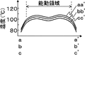
- 238000009826 distribution Methods 0.000 description 30
- 230000000694 effects Effects 0.000 description 10
- 239000004065 semiconductor Substances 0.000 description 5
- 230000015556 catabolic process Effects 0.000 description 4
- 230000020169 heat generation Effects 0.000 description 4
- 238000002955 isolation Methods 0.000 description 4
- 238000000034 method Methods 0.000 description 4
- 230000006378 damage Effects 0.000 description 3
- 238000000605 extraction Methods 0.000 description 3
- 150000004767 nitrides Chemical class 0.000 description 3
- 230000006866 deterioration Effects 0.000 description 2
- 238000005468 ion implantation Methods 0.000 description 2
- 238000004519 manufacturing process Methods 0.000 description 2
- 238000007796 conventional method Methods 0.000 description 1
- 230000002542 deteriorative effect Effects 0.000 description 1
- 239000000463 material Substances 0.000 description 1
Images



Landscapes
- Junction Field-Effect Transistors (AREA)
Description
前記一領域内に設けられた導電性を有する能動領域と、
前記能動領域のゲート電極の延在方向中央部に設けられる非導電領域とを含み、
前記各ゲート電極に対するゲート電極の延在方向における前記非導電領域が占める割合が、前記ゲート電極の配列方向における端部よりも中央部分において大きいことを特徴としている。
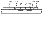
図1は本発明の第一の実施形態の電界効果トランジスタ(FET)について、電極と能動層部分の平面構成を説明するため透視して示す平面図であり、図2は、図1のFETのb−b'断面図である。
本発明の第二の実施形態は、能動領域を、非導電領域の周囲に連続的に設けることで、能動領域において、並設した複数の単位電界効果トランジスタに対して、端部の単位電界効果トランジスタほど非導電領域を小さくした結果、両端の1本または数本の単位電界効果トランジスタに設ける非導電領域の長さを0(ゼロ)、すなわち両端の1本または数本の電界効果トランジスタに対しては非導電領域を設けない構造としたものである。
第一の実施形態および第二の実施形態においては、ゲート電極の配列方向における中央部分から端部にかけて徐々に小さくなるようにする態様、例えば能動領域の中央付近に設ける非導電領域の形状を楕円形とする態様を説明してきたが、各ゲート電極に対するゲート電極の延在方向における非導電領域が占める割合が、ゲート電極の配列方向における端部よりも中央部分において大きくなるような態様であれば、これに限定されない。
図5に示すように、電極配置は第一および第二の実施形態でも説明したような櫛形電極構造であることが好ましい。すなわち、能動領域401においては、所定の間隔で並べられたゲート電極402を複数個配置するとともに、これら複数のゲート電極402間にソース電極403およびドレイン電極404を各々交互に配置する。各々のゲート電極402はバス配線405によりゲート引き出し電極406と接続され、同様にソース電極403およびドレイン電極404は各々引き出し電極407、408に集められ、接続されている。
102、302、402、502、702 ゲート電極
103、303、403、503、703 ソース電極
104、304、404、504、704 ドレイン電極
105、305、405、505、705 バス配線
106、306、406、506、706 ゲート引き出し電極
107、307、407、507、707 ソース引き出し電極
108、308、408、508、708 ドレイン引き出し電極
309、409、509、709 非導電領域
409a、409b、409c 非導電領域
Claims (2)
- 基板上の一領域内に並列配置された複数のゲート電極と、
前記一領域内に設けられ、不純物がドープされたことにより導電性を有する能動領域と、
前記能動領域のゲート電極の延在方向中央部に設けられ、不純物がドープされていない非導電領域とを含み、
前記各ゲート電極に対するゲート電極の延在方向における前記非導電領域が占める割合が、前記ゲート電極の配列方向における端部よりも中央部分において大きく、
前記能動領域が、前記非導電領域の周囲に連続的に設けられていることを特徴とする電界効果トランジスタ。 - 請求項1に記載の電界効果トランジスタにおいて、
前記各ゲート電極に対するゲート電極の延在方向における前記非導電領域が占める割合は、前記ゲート電極の配列方向における中央部分から端部にかけて徐々に小さくなることを特徴とする電界効果トランジスタ。
Priority Applications (1)
| Application Number | Priority Date | Filing Date | Title |
|---|---|---|---|
| JP2005309350A JP5114839B2 (ja) | 2005-10-25 | 2005-10-25 | 電界効果トランジスタ |
Applications Claiming Priority (1)
| Application Number | Priority Date | Filing Date | Title |
|---|---|---|---|
| JP2005309350A JP5114839B2 (ja) | 2005-10-25 | 2005-10-25 | 電界効果トランジスタ |
Publications (2)
| Publication Number | Publication Date |
|---|---|
| JP2007123304A JP2007123304A (ja) | 2007-05-17 |
| JP5114839B2 true JP5114839B2 (ja) | 2013-01-09 |
Family
ID=38146864
Family Applications (1)
| Application Number | Title | Priority Date | Filing Date |
|---|---|---|---|
| JP2005309350A Expired - Fee Related JP5114839B2 (ja) | 2005-10-25 | 2005-10-25 | 電界効果トランジスタ |
Country Status (1)
| Country | Link |
|---|---|
| JP (1) | JP5114839B2 (ja) |
Families Citing this family (1)
| Publication number | Priority date | Publication date | Assignee | Title |
|---|---|---|---|---|
| JP5728842B2 (ja) * | 2010-07-27 | 2015-06-03 | 住友電気工業株式会社 | 半導体装置 |
Family Cites Families (3)
| Publication number | Priority date | Publication date | Assignee | Title |
|---|---|---|---|---|
| JP2914411B2 (ja) * | 1992-03-30 | 1999-06-28 | 日本電気株式会社 | 電界効果トランジスタ |
| JPH08162475A (ja) * | 1994-12-02 | 1996-06-21 | Murata Mfg Co Ltd | 電界効果トランジスタ |
| JP3147048B2 (ja) * | 1997-09-12 | 2001-03-19 | 日本電気株式会社 | 半導体装置 |
-
2005
- 2005-10-25 JP JP2005309350A patent/JP5114839B2/ja not_active Expired - Fee Related
Also Published As
| Publication number | Publication date |
|---|---|
| JP2007123304A (ja) | 2007-05-17 |
Similar Documents
| Publication | Publication Date | Title |
|---|---|---|
| JP5797082B2 (ja) | 熱スペーサを有する半導体デバイス | |
| JP5106041B2 (ja) | 半導体装置 | |
| US10361271B2 (en) | Semiconductor device and method of manufacturing the same | |
| JP2002531940A (ja) | 電界効果半導体装置 | |
| US7019361B2 (en) | Semiconductor device and method of fabricating the same | |
| JP6356803B2 (ja) | 絶縁ゲートバイポーラトランジスタ | |
| CN103650141A (zh) | 超结半导体装置 | |
| JP2001028425A (ja) | 半導体装置及びその製造方法 | |
| JP2002540602A (ja) | トレンチゲート電界効果型素子を備えた電子装置 | |
| CN110120392A (zh) | 碳化硅半导体装置 | |
| JP2025120428A (ja) | 半導体スイッチングデバイス | |
| JP4966351B2 (ja) | 半導体装置 | |
| JP2008244295A (ja) | 半導体装置 | |
| US7495286B2 (en) | High-voltage semiconductor device structure | |
| US10460931B2 (en) | Semiconductor transistor having superlattice structures | |
| JP5114839B2 (ja) | 電界効果トランジスタ | |
| US9882043B2 (en) | Semiconductor device with trench termination structure | |
| JP2002110988A (ja) | 半導体装置 | |
| KR102030465B1 (ko) | 레터럴 타입의 전력 반도체 소자 | |
| CN100470832C (zh) | 半导体器件 | |
| KR102030463B1 (ko) | 레터럴 타입의 전력 반도체 소자 | |
| US20150364585A1 (en) | Power semiconductor device | |
| CN105097890A (zh) | 线型架构的功率半导体元件 | |
| JP7810487B2 (ja) | 半導体スイッチングデバイス | |
| CN113471272B (zh) | 半导体装置 |
Legal Events
| Date | Code | Title | Description |
|---|---|---|---|
| A621 | Written request for application examination |
Free format text: JAPANESE INTERMEDIATE CODE: A621 Effective date: 20080919 |
|
| A977 | Report on retrieval |
Free format text: JAPANESE INTERMEDIATE CODE: A971007 Effective date: 20120307 |
|
| A131 | Notification of reasons for refusal |
Free format text: JAPANESE INTERMEDIATE CODE: A131 Effective date: 20120403 |
|
| A521 | Written amendment |
Free format text: JAPANESE INTERMEDIATE CODE: A523 Effective date: 20120518 |
|
| TRDD | Decision of grant or rejection written | ||
| A01 | Written decision to grant a patent or to grant a registration (utility model) |
Free format text: JAPANESE INTERMEDIATE CODE: A01 Effective date: 20120918 |
|
| A01 | Written decision to grant a patent or to grant a registration (utility model) |
Free format text: JAPANESE INTERMEDIATE CODE: A01 |
|
| A61 | First payment of annual fees (during grant procedure) |
Free format text: JAPANESE INTERMEDIATE CODE: A61 Effective date: 20121001 |
|
| R150 | Certificate of patent or registration of utility model |
Free format text: JAPANESE INTERMEDIATE CODE: R150 |
|
| FPAY | Renewal fee payment (event date is renewal date of database) |
Free format text: PAYMENT UNTIL: 20151026 Year of fee payment: 3 |
|
| LAPS | Cancellation because of no payment of annual fees |