JP5116653B2 - BANDPASS FILTER, RADIO COMMUNICATION MODULE AND RADIO COMMUNICATION DEVICE USING THE SAME - Google Patents
BANDPASS FILTER, RADIO COMMUNICATION MODULE AND RADIO COMMUNICATION DEVICE USING THE SAME Download PDFInfo
- Publication number
- JP5116653B2 JP5116653B2 JP2008326987A JP2008326987A JP5116653B2 JP 5116653 B2 JP5116653 B2 JP 5116653B2 JP 2008326987 A JP2008326987 A JP 2008326987A JP 2008326987 A JP2008326987 A JP 2008326987A JP 5116653 B2 JP5116653 B2 JP 5116653B2
- Authority
- JP
- Japan
- Prior art keywords
- resonance
- electrode
- resonators
- resonator
- input
- Prior art date
- Legal status (The legal status is an assumption and is not a legal conclusion. Google has not performed a legal analysis and makes no representation as to the accuracy of the status listed.)
- Expired - Fee Related
Links
Images




Landscapes
- Control Of Motors That Do Not Use Commutators (AREA)
Description
本発明は、バンドパスフィルタならびにそれを用いた無線通信モジュールおよび無線通信機器に関するものであり、特に、広帯域化が可能で通過帯域の設計の自由度が大きい2つの通過帯域を有するバンドパスフィルタならびにそれを用いた無線通信モジュールおよび無線通信機器に関するものである。 The present invention relates to a band-pass filter, a wireless communication module and a wireless communication device using the same, and more particularly, a band-pass filter having two pass bands that can be broadened and has a high degree of freedom in designing a pass band, and The present invention relates to a wireless communication module and a wireless communication device using the same.
通信機器等の電子装置においては、特定の周波数の電気信号のみを通過させるバンドパスフィルタが用いられており、特に、同一の共振周波数を有する2つの共振器が電磁気的に結合された共振系における偶モード共振および奇モード共振を利用して、偶モード共振周波数および奇モード共振周波数を含む通過帯域を形成したバンドパスフィルタが広く用いられている。このようなバンドパスフィルタにおいては、2つの共振器間の電磁気的な結合の強さに応じて偶モード共振周波数と奇モード共振周波数との差が変化し、これによって通過帯域の幅が決定される(例えば、特許文献1を参照。)。
しかしながら、上述した従来のバンドパスフィルタは、偶モード共振および奇モード共振の2つの共振ピークを利用して通過帯域を形成するため広帯域化には限界があった。また、同一の共振周波数を有する3つの共振器が電磁気的に結合された共振系における3つの共振モードによる3つの共振ピークを利用して通過帯域を形成したバンドパスフィルタも知られており、このようなバンドパスフィルタは更なる広帯域化が可能であるが、3つの共振ピークの周波数をそれぞれ任意に設定することは困難であり、通過帯域の設計の自由度が小さいものであった。 However, the above-described conventional band-pass filter has a limit in widening the band because the pass band is formed using two resonance peaks of even mode resonance and odd mode resonance. Also known is a bandpass filter in which a pass band is formed by using three resonance peaks in three resonance modes in a resonance system in which three resonators having the same resonance frequency are electromagnetically coupled. Such a bandpass filter can be further broadened, but it is difficult to arbitrarily set the frequencies of the three resonance peaks, and the degree of freedom in designing the passband is small.
また、デュアルモードの通信装置等においては、2つの通信帯域をそれぞれ通過帯域とする2つのバンドパスフィルタが用いられており、通信装置の小型化を妨げていた。 Further, in a dual mode communication device or the like, two band pass filters each having two communication bands as pass bands are used, which hinders miniaturization of the communication device.
本発明はこのような従来の技術における問題点に鑑みて案出されたものであり、その目的は、広帯域化が可能で通過帯域の設計の自由度が大きい2つの通過帯域を備えるバンドパスフィルタならびにそれを用いた無線通信モジュールおよび無線通信機器を提供することにある。 The present invention has been devised in view of such problems in the prior art, and an object of the present invention is to provide a band-pass filter having two pass bands that can be widened and has a high degree of freedom in designing the pass band. And providing a wireless communication module and a wireless communication device using the same.
本発明のバンドパスフィルタは、複数の誘電体層が積層されてなる積層体と、該積層体の上面および下面の少なくとも一方に配置された接地電極と、前記積層体の第1の層間に相互に電磁界結合するように横並びに順次配置された、それぞれ一方端が接地されて第1乃至第3の共振器を構成する帯状の第1乃至第3の共振電極と、前記積層体の第2の層間に相互に電磁界結合するように横並びに配置された、それぞれ一方端が接地されて第4および第5の共振器を構成する帯状の第4および第5の共振電極と、前記積層体の前記第1および第2の層間の間に位置する層間に配置された、前記第1および第4の共振電極と対向して電磁界結合する帯状の第1の入出力結合電極と、前記積層体の前記第1および第2の層間の間に位置する層間に配置された、前記第2および第5の共振電極と対向して電磁界結合する帯状の第2の入出力結合電極と、前記積層体の前記第1の層間を間に挟んで前記第1の入出力結合電極が配置された層間および前記第2の入出力結合電極が配置された層間と反対側に位置する層間に配置された、自身を介して前記第1および第3の共振電極を電磁界結合させる共振器結合電極とを備え、前記第1および第2の共振器の共振周波数は互いに等しく且つ前記第3の共振器の共振周波数と異なる周波数に設定されており、前記第4および第5の共振器の共振周波数は互いに等しく且つ前記第1乃至第3の共振器の共振周波数と異なる周波数に設定されており、前記第1乃至第3の共振器を用いて第1の通過帯域を形成するとともに前記第4および第5の共振器を用いて第2の通過帯域を形成することを特徴とするものである。 The band-pass filter of the present invention includes a laminated body in which a plurality of dielectric layers are laminated, a ground electrode disposed on at least one of an upper surface and a lower surface of the laminated body, and a first layer of the laminated body. Are arranged side by side so as to be electromagnetically coupled to each other, and each of the first to third resonance electrodes in the form of first to third resonators, each of which is grounded at one end thereof, and the second of the laminate. 4th and 5th resonance electrodes, which are arranged side by side so as to be electromagnetically coupled to each other between the layers, and constitute one of the fourth and fifth resonators with one end grounded, and the laminate A band-shaped first input / output coupling electrode disposed between the first and second layers and electromagnetically coupled to face the first and fourth resonance electrodes; and the laminated layer Between the first and second layers of the body The second input / output coupling electrode in the form of a strip that is electromagnetically coupled to face the second and fifth resonance electrodes, and the first input layer sandwiching the first layer of the laminate. The first and third resonance electrodes are disposed in an electromagnetic field through the layers disposed between the layer where the output coupling electrode is disposed and the layer located on the opposite side of the layer where the second input / output coupling electrode is disposed. A resonator coupling electrode to be coupled, wherein the resonance frequencies of the first and second resonators are set to be equal to each other and different from the resonance frequency of the third resonator; The resonance frequencies of the resonators are set equal to each other and different from the resonance frequencies of the first to third resonators, and a first passband is formed using the first to third resonators. And the fourth and fifth resonators It is intended to and forming a second pass band are.
また、本発明のバンドパスフィルタは、上記構成において、前記第1乃至第3の共振電極は、それぞれの接地される側が互い違いになるように配置されており、前記共振器結合電極を介した前記第1および第3の共振電極の電磁界結合は主に容量性の結合とされており、前記第1および第2の共振器の共振周波数は前記第3の共振器の共振周波数よりも高く設定されていることを特徴とするものである。 In the band-pass filter of the present invention, in the above configuration, the first to third resonance electrodes are arranged so that the grounded sides are staggered, and the band-pass filter is arranged with the resonator coupling electrode interposed therebetween. The electromagnetic coupling of the first and third resonant electrodes is mainly capacitive coupling, and the resonant frequency of the first and second resonators is set higher than the resonant frequency of the third resonator. It is characterized by being.
本発明の無線通信モジュールは、上記各構成のいずれかのバンドパスフィルタを備えることを特徴とするものである。 A wireless communication module according to the present invention includes any one of the bandpass filters having the above-described configurations.
本発明の無線通信機器は、アンテナと、該アンテナに接続された上記各構成のいずれかのバンドパスフィルタを含むRF部と、該RF部に接続されたベースバンド部とを備えることを特徴とするものである。 A wireless communication device of the present invention includes an antenna, an RF unit including the bandpass filter of any of the above-described configurations connected to the antenna, and a baseband unit connected to the RF unit. To do.
本発明のバンドパスフィルタは、相互に電磁界結合するように横並びに順次配置されて第1乃至第3の共振器を構成する第1乃至第3の共振電極と、第1および第3の共振電極を電磁界結合させる共振器結合電極とを備え、第1および第2の共振器の共振周波数は互いに等しく且つ第3の共振器の共振周波数と異なる周波数に設定されており、第1乃至第3の共振器を用いて第1の通過帯域を形成する。 The band-pass filter according to the present invention includes first to third resonance electrodes that are disposed side by side and sequentially so as to be electromagnetically coupled to each other to form first to third resonators, and first and third resonances. And a resonator coupling electrode for electromagnetically coupling the electrodes, wherein the resonance frequencies of the first and second resonators are set to be equal to each other and different from the resonance frequency of the third resonator, The first passband is formed using three resonators.
このような構成を備える本発明のバンドパスフィルタによれば、隣り合う互いに共振周波数が等しい第1および第2の共振器が電磁界結合することにより、偶モードおよび奇モードの2つの共振ピークが生じる。また、第1および第2の共振器と異なる共振周波数に設定された第3の共振器が第2の共振器と直接電磁界結合するとともに共振器結合電極を介して第1の共振器と電磁界結合することにより3つ目の共振ピークが生じる。この3つの共振ピークを用いて第1の通過帯域を形成することができるので、第1の通過帯域が広いバンドパスフィルタを得ることができる。また、3つの共振ピークの周波数を任意に設定することができるので、第1の通過帯域の設計の自由度が大きいバンドパスフィルタを得ることができる。 According to the bandpass filter of the present invention having such a configuration, the first and second resonators having the same resonance frequency adjacent to each other are electromagnetically coupled, so that two resonance peaks of the even mode and the odd mode are generated. Arise. In addition, the third resonator set at a different resonance frequency from the first and second resonators is directly electromagnetically coupled to the second resonator and electromagnetically coupled to the first resonator via the resonator coupling electrode. A third resonance peak is generated by the field coupling. Since the first passband can be formed using these three resonance peaks, a bandpass filter having a wide first passband can be obtained. In addition, since the frequencies of the three resonance peaks can be set arbitrarily, a bandpass filter having a high degree of freedom in designing the first passband can be obtained.
また、本発明のバンドパスフィルタによれば、第4および第5の共振器を構成する第4および第5の共振電極と、第1および第4の共振電極と対向して電磁界結合する帯状の第1の入出力結合電極と、第2および第5の共振電極と対向して電磁界結合する帯状の第2の入出力結合電極とを備え、第4および第5の共振器の共振周波数は互いに等しく且つ第1乃至第3の共振器の共振周波数と異なる周波数に設定されており、第4および第5の共振器を用いて第2の通過帯域を形成する。 In addition, according to the bandpass filter of the present invention, the fourth and fifth resonance electrodes constituting the fourth and fifth resonators, and the band-like shape that is electromagnetically coupled to face the first and fourth resonance electrodes. A first input / output coupling electrode and a band-like second input / output coupling electrode facing the second and fifth resonance electrodes and electromagnetically coupled to each other, and the resonance frequencies of the fourth and fifth resonators Are set to be equal to each other and different from the resonance frequencies of the first to third resonators, and form the second passband using the fourth and fifth resonators.
このような構成を備える本発明のバンドパスフィルタによれば、第1乃至第3の共振器を用いて形成される第1の通過帯域に加えて、第4および第5の共振器を用いて形成される第2の通過帯域を備えるため、2つの通過帯域を有するバンドパスフィルタを得ることができる。また、第1の入出力結合電極は第1および第4の共振電極と対向して電磁界結合し、第2の入出力結合電極は第2および第5の共振電極と対向して電磁界結合することから、2つの通過帯域を形成する2つの共振系と入出力とのインピーダンス整合を広い周波数帯域に渡って良好に保つことができるので、2つの広い通過帯域を備えるバンドパスフィルタを得ることが可能となる。 According to the bandpass filter of the present invention having such a configuration, in addition to the first passband formed using the first to third resonators, the fourth and fifth resonators are used. Since the second passband is formed, a bandpass filter having two passbands can be obtained. The first input / output coupling electrode is electromagnetically coupled to face the first and fourth resonance electrodes, and the second input / output coupling electrode is electromagnetically coupled to face the second and fifth resonance electrodes. As a result, impedance matching between the two resonance systems forming the two pass bands and the input / output can be maintained well over a wide frequency band, so that a bandpass filter having two wide pass bands can be obtained. Is possible.
また、本発明のバンドパスフィルタによれば、第1乃至第3の共振電極は、それぞれの接地される側が互い違いになるように配置されており、共振器結合電極を介した第1および第3の共振電極の電磁界結合は主に容量性の結合とされており、第1および第2の共振器の共振周波数が第3の共振器の共振周波数よりも高く設定されているときには、第1乃至第3の共振器同士の電磁界結合が全て主に容量性の結合となり、第1の共振器から直接第2の共振器へ伝達される電気信号と第1の共振器から第3の共振器を介して第2の共振器へ伝達される信号との間において、3つの共振ピークの間の周波数では位相反転が生じず、3つの共振ピークの外側の周波数で位相反転が生じるので、第1の通過帯域において、3つの共振ピークを含む通過帯域内には減衰極がなく、3つの共振ピークの外側の通過帯域外に減衰極を有する優れた通過特性を有するバンドパスフィルタを得ることができる。 According to the bandpass filter of the present invention, the first to third resonance electrodes are arranged so that the grounded sides are staggered, and the first and third resonance electrodes are interposed via the resonator coupling electrodes. The electromagnetic coupling of the resonant electrodes is mainly capacitive coupling. When the resonant frequency of the first and second resonators is set higher than the resonant frequency of the third resonator, The electromagnetic coupling between the third to third resonators is mainly capacitive coupling, and the electric signal transmitted directly from the first resonator to the second resonator and the third resonance from the first resonator. Since the phase inversion does not occur at the frequency between the three resonance peaks and the signal is transmitted to the second resonator through the resonator, the phase inversion occurs at the frequency outside the three resonance peaks. Pass including three resonance peaks in one passband No attenuation pole in the region, it is possible to obtain a band-pass filter having an excellent pass characteristics having three outer passband attenuation pole of the resonance peak.
本発明の無線通信モジュールおよび本発明の無線通信機器によれば、広帯域な第1の通過帯域および第2の通過帯域を有する本発明のバンドパスフィルタを通信信号の濾波に用いることにより、バンドパスフィルタを通過する通信信号の減衰を小さくすることができるので、小型で高性能な無線通信モジュールおよび無線通信機器を得ることができる。 According to the wireless communication module of the present invention and the wireless communication device of the present invention, the bandpass filter of the present invention having the first passband and the second passband having a wide band is used for filtering the communication signal. Since attenuation of the communication signal passing through the filter can be reduced, a small and high-performance wireless communication module and wireless communication device can be obtained.
以下、本発明のバンドパスフィルタならびにそれを用いた無線通信モジュールおよび無線通信機器を添付の図面を参照しつつ詳細に説明する。 Hereinafter, a bandpass filter of the present invention, a wireless communication module and a wireless communication device using the same will be described in detail with reference to the accompanying drawings.
(実施の形態の第1の例)
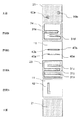
図1は本発明のバンドパスフィルタの実施の形態の第1の例を模式的に示す外観斜視図である。図2は図1に示すバンドパスフィルタの例の模式的な分解斜視図である。図3は図1に示すバンドパスフィルタの例の上下面および層間を模式的に示す平面図である。図4は図1に示すバンドパスフィルタの例のQ−Q’線断面図である。
(First example of embodiment)
FIG. 1 is an external perspective view schematically showing a first example of an embodiment of the bandpass filter of the present invention. FIG. 2 is a schematic exploded perspective view of the example of the bandpass filter shown in FIG. FIG. 3 is a plan view schematically showing upper and lower surfaces and layers of the example of the bandpass filter shown in FIG. FIG. 4 is a cross-sectional view taken along the line QQ ′ of the example of the bandpass filter shown in FIG.
本例のバンドパスフィルタは、図1〜図4に示すように、複数の誘電体層11が積層されてなる積層体10と、積層体10の上面および下面のほぼ全面に配置された接地電極21と、積層体10の層間Aに相互に電磁界結合するように横並びに順次配置された、それぞれ一方端が接地されて第1乃至第3の共振器を構成する帯状の第1乃至第3の共振電極31a,31b,31cと、積層体10の層間Bに相互に電磁界結合するように横並びに配置された、それぞれ一方端が接地されて第4および第5の共振器を構成する帯状の第4および第5の共振電極31d,31eと、積層体10の層間Aおよび層間Bの間に位置する層間Cに配置された、第1および第4の共振電極31a,31dと対向して電磁界結合する帯状の第1の入出力結合電極40aと、第2および第5の共振電極31b,31eと対向して電磁界結合する帯状の第2の入出力結合電極40bと、積層体10の層間Aを間に挟んで層間Cと反対側に位置する層間Dに配置された、自身を介して第1および第3の共振電極を電磁界結合させる共振器結合電極43とを備えている。また、積層体10の上面には第1の入出力端子電極60aおよび第2の入出力端子電極60bが接地電極21と間隔を開けて配置されており、それぞれ貫通導体50を介して第1の入出力結合電極40aおよび第2の入出力結合電極40bに接続されている。そして、積層体10の層間Aには、第1乃至第3の共振電極31a,31b,31cの周囲を囲むように第1の環状接地電極23が配置されており、第1乃至第3の共振電極31a,31b,31cの一方端がそれぞれ接続されている。また、積層体10の層間Bには、第4および第5の共振電極31d,31eの周囲を囲むように第2の環状接地電極24が配置されており、第4および第5の共振電極31d,31eの一方端がそれぞれ接続されている。なお、第1乃至第3の共振電極31a,31b,31cはそれぞれの一方端が互い違いになるように配置されており、第4および第5の共振電極31d,31eはそれぞれの一方端が互い違いになるように配置されている。
As shown in FIGS. 1 to 4, the band-pass filter of this example includes a laminated
また、本例のバンドパスフィルタにおいて、共振器結合電極43は、その一方端が貫通導体50を介して第3の共振電極31cの他方端に接続されており、第3の共振電極31cおよび貫通導体50とともに第3の共振器を構成している。また、共振器結合電極43の他方端は、誘電体層11を介して第1の共振電極31aの他方端と対向しており、第1の共振電極31aと主に容量性の電磁界結合をしている。また、第1および第2の共振器の共振周波数は互いに等しく且つ第3の共振器の共振周波数よりも高くなるように設定されており、第4および第5の共振器の共振周波数は互いに等しく且つ第1乃至第3の共振器の共振周波数よりも高くなるように設定されている。
Further, in the bandpass filter of this example, the
さらに、本例のバンドパスフィルタは、第1の入出力結合電極40aにおいて電気信号が入力または出力される第1の入出力点45aは、第1の共振電極31aとの対向部の中央よりも第1の共振電極31aの他方端に近い側にあり、第4の共振電極31dとの対向部の中央よりも第4の共振電極31dの他方端に近い側にある。また、第2の入出力結合電極40bにおいて電気信号が入力または出力される第2の入出力点45bは、第2の共振電極31bとの対向部の中央よりも第2の共振電極31bの他方端に近い側にあり、第5の共振電極31eとの対向部の中央よりも第5の共振電極31eの他方端に近い側にある。
Further, in the band-pass filter of this example, the first input /
このような構成を備える本例のバンドパスフィルタによれば、例えば、第1の入出力端子電極60aおよび貫通導体50を介して第1の入出力結合電極40aに外部回路からの電気信号が入力されると、第1の入出力結合電極40aと電磁界結合する第1の共振電極31aが励振されるとともに、これと電磁界結合する第2の共振電極31bが共振する。また、第1の共振電極31aが共振すると、共振器結合電極43を介して第1の共振電極31aと電磁界結合する第3の共振電極31cも共振し、そのエネルギーは第3の共振電極31cと電磁界結合する第2の共振電極31bに伝えられる。この2つのルートで第2の共振電極31bに電気信号が伝達され、第2の共振電極31bと電磁界結合する第2の入出力結合電極40bから貫通導体50および第2の入出力端子電極60bを介して外部回路に電気信号が出力される。これによって第1の通過帯域が形成される。また、第1の入出力結合電極40aと電磁界結合する第4の共振電極31dが励振されるとともに、これと電磁界結合する第5の共振電極31eが共振し、第5の共振電極31eと電磁界結合する第2の入出力結合電極40bから貫通導体50および第2の入出力端子電極60bを介して外部回路に電気信号が出力される。これによって第2の通過帯域が形成される。このようにして、本例のバンドパスフィルタは、2つの通過帯域を有するバンドパスフィルタとして機能することができる。
According to the band-pass filter of this example having such a configuration, for example, an electric signal from an external circuit is input to the first input /
また、本例のバンドパスフィルタによれば、隣り合う互いに共振周波数が等しい第1および第2の共振器が電磁界結合することにより、偶モードおよび奇モードの2つの共振ピークが生じる。また、第1および第2の共振器よりも共振周波数が低く設定された第3の共振器が第2の共振器と直接電磁界結合するとともに共振器結合電極43を介して第1の共振器と電磁界結合することにより3つ目の共振ピークが生じる。この3つの共振ピークを用いて第1の通過帯域を形成することができるので、広帯域な第1の通過帯域を有するバンドパスフィルタを得ることができる。また、3つの共振ピークの周波数を任意に設定することができるので、第1の通過帯域の設計の自由度が大きいバンドパスフィルタを得ることができる。
Further, according to the band-pass filter of this example, two adjacent resonance peaks of the even mode and the odd mode are generated by the electromagnetic coupling between the first and second resonators having the same resonance frequency. A third resonator having a resonance frequency lower than that of the first and second resonators is directly electromagnetically coupled to the second resonator, and the first resonator is connected via the
さらに、本例のバンドパスフィルタによれば、第1乃至第3の共振電極31a,31b,31cの接地される側が互い違いになるように配置されてインターデジタル型に電磁界結合しているので、第1の共振電極31aと第2の共振電極31bとの電磁界結合および第2の共振電極31bと第3の共振電極31cとの電磁界結合はどちらも主に容量性の結合になる。そして、第1の共振電極31aと第3の共振電極31cとは共振器結合電極43を介して容量性主体で電磁界結合しているので、第1乃至第3の共振器間の電磁界結合は全て主に容量性の結合となっている。その上で、第1および第2の共振器の共振周波数が第3の共振器の共振周波数よりも高く設定されていることから、第1の共振器から直接第2の共振器へ伝達される電気信号と第1の共振器から第3の共振器を介して第2の共振器へ伝達される信号との間において、3つの共振ピークの間の周波数では位相反転が生じず、3つの共振ピークの外側の周波数で位相反転が生じるので、3つの共振ピークを含む第1の通過帯域内には減衰極がなく、3つの共振ピークの外側の通過帯域外に減衰極を有する優れた通過特性を有するバンドパスフィルタを得ることができる。
Furthermore, according to the bandpass filter of this example, the grounded sides of the first to
(実施の形態の第2の例)
図5は本発明のバンドパスフィルタの実施の形態の第2の例を模式的に示す分解斜視図である。なお、本例においては前述した第1の例と異なる点のみについて説明し、同様の構成要素については同一の参照符号を用いて重複する説明を省略する。
(Second example of embodiment)
FIG. 5 is an exploded perspective view schematically showing a second example of the embodiment of the bandpass filter of the present invention. Note that in this example, only differences from the first example described above will be described, and the same components will be denoted by the same reference numerals, and redundant description will be omitted.
本例のバンドパスフィルタは、図5に示すように、積層体10の層間Bに、第4の共振電極31dを間に挟んで第5の共振電極31eと反対側に第6の共振電極31fが配置されている。第6の共振電極31fは、その一方端が第2の環状接地電極24に接続されて接地されている。また、積層体10の層間Bを間に挟んで層間Cと反対側に位置する層間Eに、第2の共振器結合電極44が配置されており、その一方端が貫通導体50を介して第6の共振電極31fの他方端に接続されており、第6の共振電極31fおよび貫通導体50とともに第6の共振器を構成している。また、第2の共振器結合電極44の他方端は、誘電体層11を介して第5の共振電極31eの他方端と対向しており、第5の共振電極31eと主に容量性の電磁界結合をしている。また、第6の共振器の共振周波は、第1乃至第3の共振器の共振周波数よりは高く、第4および第5の共振器の共振周波数よりは低くなるように設定されており、第4乃至第6の共振器で第2の通過帯域を形成するようにされている。
As shown in FIG. 5, the band-pass filter of this example has a
このような構成を備える本例のバンドパスフィルタによれば、第4および第5の共振器が電磁界結合することにより、偶モードおよび奇モードの2つの共振ピークが生じる。そして、第6の共振器が第4の共振器と直接電磁界結合するとともに第2の共振器結合電極44を介して第5の共振器と電磁界結合することにより3つ目の共振ピークが生じる。この3つの共振ピークを用いて第2の通過帯域を形成することができるので、広帯域な第2の通過帯域を有するバンドパスフィルタを得ることができる。また、3つの共振ピークの周波数を任意に設定することができるので、第2の通過帯域の設計の自由度が大きいバンドパスフィルタを得ることができる。
According to the band-pass filter of this example having such a configuration, the fourth and fifth resonators are electromagnetically coupled to generate two resonance peaks of an even mode and an odd mode. The sixth resonator is directly electromagnetically coupled to the fourth resonator and electromagnetically coupled to the fifth resonator via the second
さらに、本例のバンドパスフィルタによれば、第4乃至第6の共振電極31d,31e,31fの接地される側が互い違いになるように配置されてインターデジタル型に電磁界結合しているので、第4の共振電極31dと第5の共振電極31eとの電磁界結合および第4の共振電極31dと第6の共振電極31fとの電磁界結合はどちらも主に容量性の結合になる。そして、第5の共振電極31eと第6の共振電極31fとが第2の共振器結合電極44を介して主に容量性の結合をしているので、第4乃至第6の共振器間の電磁界結合は全て主に主に容量性の結合となっている。その上で、第4および第5の共振器の共振周波数が第6の共振器の共振周波数よりも高く設定されていることから、第4の共振器から直接第5の共振器へ伝達される電気信号と第4の共振器から第6の共振器を介して第5の共振器へ伝達される信号との間において、3つの共振ピークの間の周波数では位相反転が生じず、3つの共振ピークの外側の周波数で位相反転が生じるので、3つの共振ピークを含む第2の通過帯域内には減衰極がなく、3つの共振ピークの外側の通過帯域外に減衰極を有する優れた通過特性を有するバンドパスフィルタを得ることができる。
Furthermore, according to the bandpass filter of this example, the grounded sides of the fourth to
(実施の形態の第3の例)
図6は本発明のバンドパスフィルタの実施の形態の第3の例を模式的に示す外観斜視図である。図7は図6に示すバンドパスフィルタの例の模式的な分解斜視図である。図8は図6に示すバンドパスフィルタの例の上下面および層間を模式的に示す平面図である。なお、本例においては前述した第1の例と異なる点のみについて説明し、同様の構成要素については同一の参照符号を用いて重複する説明を省略する。
(Third example of embodiment)
FIG. 6 is an external perspective view schematically showing a third example of the embodiment of the bandpass filter of the present invention. FIG. 7 is a schematic exploded perspective view of the example of the bandpass filter shown in FIG. FIG. 8 is a plan view schematically showing the upper and lower surfaces and the layers of the example of the bandpass filter shown in FIG. Note that in this example, only differences from the first example described above will be described, and the same components will be denoted by the same reference numerals, and redundant description will be omitted.
本例のバンドパスフィルタにおいては、図6〜図8に示すように、第1の入出力端子電極60aおよび第2の入出力端子電極60bが積層体10の対向する2側面に分かれて配置されており、積層体10の他の2側面には接地電極21に接続される接地端子電極60cが配置されている。そして、第1の環状接地電極23に代えて第1の共振電極31aおよび第3の共振電極31cの一方端が接続された内層接地電極23aと第2の共振電極31bの一方端が接続された内層接地電極23bが第1の層間に配置されており、内層接地電極23aおよび内層接地電極23bは積層体10の側面に配置された接地端子電極60cに接続されている。
In the bandpass filter of this example, as shown in FIGS. 6 to 8, the first input /
また、本例のバンドパスフィルタにおいては、第1の入出力結合電極40aは、積層体10の層間Aと層間Bとの間に位置する層間Cに配置された第1部分41aと、層間Cと層間Bとの間に位置する層間Fに配置された第2部分42aとの2層に分離されて配置されている。第1部分41aおよび第2部分42aは、それぞれの一方端が積層体10の側面に配置された第1の入出力端子電極60aに接続されており、それぞれの他方端は、それぞれの間に位置する誘電体層11を貫通する貫通導体50によって互いに接続されている。同様に、第2の入出力結合電極40bは、積層体10の層間Cに配置された第1部分41bと、層間Fに配置された第2部分42bとの2層に分離されて配置されている。第1部分41bおよび第2部分42bは、それぞれの一方端が積層体10の側面に配置された第2の入出力端子電極60bに接続されており、それぞれの他方端は、それぞれの間に位置する誘電体層11を貫通する貫通導体50によって互いに接続されている。
In the bandpass filter of this example, the first input /
さらに、本例のバンドパスフィルタにおいては、第2の環状接地電極24が設けられておらず、第4の共振電極31dの一方端は積層体10の側面に配置された接地端子電極60cに接続されており、第5の共振電極31eの一方端は、誘電体層11を貫通する貫通導体50を介して内層接地電極23bに接続されている。そして、第1の共振電極31aの他方端は貫通導体50を介して層間Dに配置された共振器結合電極43の一方端に接続されており、共振器結合電極43の他方端は間に位置する誘電体層11を介して第3の共振電極31cの他方端と対向して主に容量性の電磁界結合をしている。また、層間Dを間に挟んで層間Aと反対側に位置する層間Hには、接地端子電極60cに接続された内層接地電極22aが配置されている。そして、層間Hと積層体10の下面との間に位置する層間Jには、層間Hに配置された内層接地電極22aおよび積層体10の下面に配置された接地電極21と誘電体層11を介して対向する第1の容量電極35aが配置されている。第1の容量電極35aは貫通導体50を介して共振器結合電極43に接続されており、共振器結合電極43および第1の共振電極31aとともに第1の共振器を構成している。
Further, in the band pass filter of this example, the second
またさらに、本例のバンドパスフィルタにおいては、積層体10の層間Hに接地端子電極60cに接続された内層接地電極22bが配置されており、層間Jには、層間Hに配置された内層接地電極22bおよび積層体10の下面に配置された接地電極21と誘電体層11を介して対向する第2の容量電極35bが配置されている。第2の容量電極35bは、貫通導体50および層間Dに配置された接続電極36を介して第2の共振電極31bの他方端に接続されており、貫通導体50,接続電極36および第2の共振電極31bとともに第2の共振器を構成している。
Furthermore, in the band pass filter of this example, the inner
さらにまた、本例のバンドパスフィルタにおいては、積層体10の層間Bと上面との間に位置する層間Eに、接地端子電極60cに接続された内層接地電極22cが配置されている。また、層間Eと積層体10の上面との間に位置する層間Gに、層間Eに配置された内層接地電極22cおよび積層体の上面に配置された接地電極21と誘電体層11を介して対向する第3の容量電極35cが配置されている。第3の容量電極35cは、貫通導体50を介して第3の共振電極31cの他方端に接続されており、貫通導体50および第3の共振電極31cとともに第3の共振器を構成している。
Furthermore, in the band-pass filter of this example, the inner
このような構成を備える本例のバンドパスフィルタによれば、第1の入出力結合電極40aおよび第2の入出力結合電極40bが2層に分離されていることから、第1および第2の共振電極31a,31bならびに第4および第5の共振電極31d,31eと第1の入出力結合電極40aおよび第2の入出力結合電極40bとの間隔を維持したままで、第1および第2の共振電極31a,31bと第4および第5の共振電極31d,31eとの間隔を広げることができる。これにより、第1および第2の共振電極31a,31bならびに第4および第5の共振電極31d,31eと第1の入出力結合電極40aおよび第2の入出力結合電極40bとの電磁界結合を強めることができるので、第1および第2の通過帯域が広い場合においても、通過帯域の全体に渡って入出力インピーダンスが良好に整合された、平坦な通過帯域を有するバンドパスフィルタを得ることができる。
According to the bandpass filter of this example having such a configuration, the first input /
また、本例のバンドパスフィルタによれば、第1の容量電極35aと内層接地電極22aおよび接地電極21との間に生じる静電容量ならびに共振器結合電極43および貫通導体50が有するインダクタンスにより、第1の共振電極31aの長さを短縮することができる。また、第2の容量電極35bと内層接地電極22bおよび接地電極21との間に生じる静電容量ならびに第2の容量電極35b,接続電極36および貫通導体50が有するインダクタンスにより、第2の共振電極31bの長さを短縮することができる。さらに、第3の共振電極31cと内層接地電極22cおよび接地電極21との間に生じる静電容量ならびに第3の容量電極35cおよび貫通導体50が有するインダクタンスにより、第3の共振電極31cの長さを短縮することができる。よって、小型のバンドパスフィルタを得ることができる。
Further, according to the band-pass filter of this example, due to the capacitance generated between the
(実施の形態の第4の例)
図9は本発明のバンドパスフィルタを用いた無線通信モジュール80および無線通信機器85の構成例を示すブロック図である。
(Fourth example of embodiment)
FIG. 9 is a block diagram showing a configuration example of the
本発明の無線通信モジュール80は、例えば、ベースバンド信号が処理されるベースバンド部81と、ベースバンド部81に接続されベースバンド信号の変調後および復調前のRF信号が処理されるRF部82とを備えている。RF部82には前述の本発明のバンドパスフィルタ821が含まれており、ベースバンド信号が変調されてなるRF信号または受信したRF信号における通信帯域以外の信号をバンドパスフィルタ821によって減衰させている。具体的な構成としては、ベースバンド部81にはベースバンドIC 811が配置され、RF部82にはバンドパスフィルタ821とベースバンド部81との間にRF IC 822が配置されている。なお、これらの回路間には別の回路が介在していてもよい。そして、無線通信モジュール80のバンドパスフィルタ821にアンテナ84を接続することによってRF信号の送受信がなされる本発明の無線通信機器85が構成される。
The
このような構成を有する本例の無線通信モジュール80および無線通信機器85によれば、広帯域な第1の通過帯域および第2の通過帯域を有する本発明の821を送信信号および受信信号の濾波に用いることにより、バンドパスフィルタ821を通過する受信信号および送信信号の減衰が少なくなるため、受信感度が向上し、また、送信信号および受信信号の増幅度を小さくできるため増幅回路における消費電力が少なくなる。また、2つの通過帯域の濾波を1つのバンドパスフィルタで行うことができる。よって、受信感度が高く消費電力が少ない小型で高性能の無線通信モジュール80および無線通信機器85を得ることができる。
According to the
本発明のバンドパスフィルタにおいて、誘電体層11の材質としては、例えばエポキシ樹脂等の樹脂や例えば誘電体セラミックス等のセラミックスを用いることができる。例えば、BaTiO3,Pb4Fe2Nb2O12,TiO2等の誘電体セラミック材料と、B2O3,SiO2,Al2O3,ZnO等のガラス材料とからなり、800〜1200℃程度の比較的低い温度で焼成が可能なガラス−セラミック材料が好適に用いられる。また、誘電体層11の厚みとしては、例えば0.01〜0.1mm程度に設定される。
In the band-pass filter of the present invention, as the material of the
前述した各種の電極および貫通導体の材質としては、例えば、Ag,Ag−Pd,Ag−Pt等のAg合金を主成分とする導電材料やCu系,W系,Mo系,Pd系導電材料等が好適に用いられる。各種の電極の厚みは、例えば0.001〜0.2mmに設定される。 Examples of the materials for the various electrodes and through conductors described above include conductive materials mainly composed of Ag alloys such as Ag, Ag-Pd, and Ag-Pt, Cu-based, W-based, Mo-based, and Pd-based conductive materials. Are preferably used. The thickness of various electrodes is set to 0.001 to 0.2 mm, for example.
本発明のバンドパスフィルタは、例えば次のようにして作製することができる。まず、セラミック原料粉末に適当な有機溶剤等を添加・混合して泥漿を作製するとともに、ドクターブレード法によってセラミックグリーンシートを形成する。次に、得られたセラミックグリーンシートにパンチングマシーン等を用いて貫通導体を形成するための貫通孔を形成し、Ag,Ag−Pd,Au,Cu等の導体を含む導体ペーストを充填するとともにセラミックグリーンシートの表面に印刷法を用いて前述したのと同様の導体ペーストを塗布して導体ペースト付きセラミックグリーンシートを作製する。次に、これらの導体ペースト付きセラミックグリーンシートを積層し、ホットプレス装置を用いて圧着し、800℃〜1050℃程度のピーク温度で焼成することにより作製される。 The bandpass filter of the present invention can be manufactured, for example, as follows. First, an appropriate organic solvent or the like is added to and mixed with the ceramic raw material powder to produce a slurry, and a ceramic green sheet is formed by a doctor blade method. Next, a through hole for forming a through conductor is formed on the obtained ceramic green sheet using a punching machine or the like, and a conductive paste containing a conductor such as Ag, Ag-Pd, Au, Cu is filled and the ceramic The same conductive paste as described above is applied to the surface of the green sheet using a printing method to produce a ceramic green sheet with a conductive paste. Next, these ceramic green sheets with a conductive paste are laminated, pressed using a hot press device, and fired at a peak temperature of about 800 ° C. to 1050 ° C.
次に、本発明のバンドパスフィルタの具体例について説明する。 Next, a specific example of the bandpass filter of the present invention will be described.
図6〜図8に示した実施の形態の第3の例のバンドパスフィルタの電気特性を、有限要素法を用いたシミュレーションによって算出した。 The electrical characteristics of the bandpass filter of the third example of the embodiment shown in FIGS. 6 to 8 were calculated by simulation using the finite element method.
本シミュレーションにおいては、第1の共振電極31aは幅が0.34mmで長さが1.6mmの矩形状とした。第2の共振電極31bは幅が0.34mmで長さが1.9mmの矩形状とした。第3の共振電極31cは幅が0.34mmで長さが2.0mmの矩形状とした。第1の容量電極35aは幅が0.29mmで長さが0.7mmの矩形状とした。第2の容量電極35bは幅が0.3mmで長さが1.0mmの矩形状とした。第3の容量電極35cは幅が0.73mmで長さが0.63mmの矩形状とした。第4の共振電極31dは幅が0.15mmで長さが1.5mmの矩形状とした。第5の共振電極31eは幅が0.15mmで長さが1.55mmの矩形状とした。第1の入出力結合電極40aの第1部分41aは幅が0.09mmで長さが1.9mmの矩形状とし、第2部分42aは幅が0.14mmで長さが1.9mmの矩形状とした。第2の入出力結合電極40bの第1部分41bは幅が0.09mmで長さが1.75mmの矩形状とし、第2部分42bは幅が0.09mmで長さが1.75mmの矩形状とした。バンドパスフィルタ全体は幅が2.0mmで長さが2.5mmで高さが0.9mmの直方体状とし、誘電体層11の比誘電率は18.7とした。
In this simulation, the
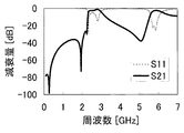
図10はそのシミュレーション結果を示すグラフであり、横軸は周波数,縦軸は減衰量を表しており、バンドパスフィルタの通過特性(S21)および反射特性(S11)を示している。図10に示すグラフによれば、広帯域な2つの通過帯域を備えるとともに、低周波側の第1の通過帯域よりもさらに低周波側に3つの減衰極が形成されており、第1の通過帯域よりも低周波側における減衰量が充分に確保された優れた通過特性が得られていることがわかる。なお、第1の通過帯域に最も近い周波数にある減衰極は、第1〜第3の共振器が全て容量結合し、第1および第2の共振器の共振周波数が等しく且つ第3の共振器の共振周波数よりも高く設定されていることにより生じる減衰極であり、それよりも低周波側の2つの減衰極は、第1の入出力結合電極40aおよび第2の入出力結合電極40bと第3の共振器との容量性の結合ならびに第1の入出力結合電極40aと第2の入出力結合電極40bとの容量性の結合により形成されたものである。このシミュレーション結果により本発明の有効性が確認できた。
FIG. 10 is a graph showing the simulation results, where the horizontal axis represents frequency and the vertical axis represents attenuation, and shows the pass characteristic (S21) and reflection characteristic (S11) of the bandpass filter. According to the graph shown in FIG. 10, there are provided two wide passbands, and three attenuation poles are formed on the lower frequency side than the first passband on the low frequency side. It can be seen that an excellent pass characteristic with sufficient attenuation on the low frequency side is obtained. The attenuation pole located at the frequency closest to the first passband is such that the first to third resonators are all capacitively coupled, the first and second resonators have the same resonance frequency, and the third resonator. The two attenuation poles on the lower frequency side are the first input /
10:積層体
11:誘電体層
21:接地電極
31a:第1の共振電極
31b:第2の共振電極
31c:第3の共振電極
31d:第4の共振電極
31e:第5の共振電極
40a:第1の入出力結合電極
40b:第2の入出力結合電極
43:共振器結合電極
80:無線通信モジュール
81:ベースバンド部
82:RF部
84:アンテナ
85:無線通信機器
10: Laminate
11: Dielectric layer
21: Ground electrode
31a: first resonance electrode
31b: second resonant electrode
31c: third resonant electrode
31d: fourth resonant electrode
31e: Fifth resonance electrode
40a: first input / output coupling electrode
40b: second input / output coupling electrode
43: Resonator coupling electrode
80: Wireless communication module
81: Baseband
82: RF section
84: Antenna
85: Wireless communication equipment
Claims (4)
該積層体の上面および下面の少なくとも一方に配置された接地電極と、
前記積層体の第1の層間に相互に電磁界結合するように横並びに順次配置された、それぞれ一方端が接地されて第1乃至第3の共振器を構成する帯状の第1乃至第3の共振電極と、
前記積層体の第2の層間に相互に電磁界結合するように横並びに配置された、それぞれ一方端が接地されて第4および第5の共振器を構成する帯状の第4および第5の共振電極と、
前記積層体の前記第1および第2の層間の間に位置する層間に配置された、前記第1および第4の共振電極と対向して電磁界結合する帯状の第1の入出力結合電極と、
前記積層体の前記第1および第2の層間の間に位置する層間に配置された、前記第2および第5の共振電極と対向して電磁界結合する帯状の第2の入出力結合電極と、
前記積層体の前記第1の層間を間に挟んで前記第1の入出力結合電極が配置された層間および前記第2の入出力結合電極が配置された層間と反対側に位置する層間に配置された、自身を介して前記第1および第3の共振電極を電磁界結合させる共振器結合電極とを備え、
前記第1および第2の共振器の共振周波数は互いに等しく且つ前記第3の共振器の共振周波数と異なる周波数に設定されており、
前記第4および第5の共振器の共振周波数は互いに等しく且つ前記第1乃至第3の共振器の共振周波数と異なる周波数に設定されており、
前記第1乃至第3の共振器を用いて第1の通過帯域を形成するとともに前記第4および第5の共振器を用いて第2の通過帯域を形成することを特徴とするバンドパスフィルタ。 A laminate in which a plurality of dielectric layers are laminated;
A ground electrode disposed on at least one of the upper surface and the lower surface of the laminate;
The first to third belt-shaped first to third resonators are arranged side by side so as to be electromagnetically coupled to each other between the first layers of the multilayer body, and each end thereof is grounded to form first to third resonators. A resonant electrode;
Band-like fourth and fifth resonances arranged side by side so as to be electromagnetically coupled to each other between the second layers of the multilayer body and having one end grounded to form fourth and fifth resonators, respectively. Electrodes,
A band-shaped first input / output coupling electrode which is disposed between the first and second layers of the laminate and is electromagnetically coupled to face the first and fourth resonance electrodes; ,
A band-shaped second input / output coupling electrode that is disposed between the first and second layers of the laminate and is electromagnetically coupled to face the second and fifth resonance electrodes; ,
Arranged between the layer in which the first input / output coupling electrode is disposed and the layer located on the opposite side of the layer in which the second input / output coupling electrode is disposed with the first layer of the laminate interposed therebetween And a resonator coupling electrode for electromagnetically coupling the first and third resonant electrodes via itself,
The resonance frequencies of the first and second resonators are set to be equal to each other and different from the resonance frequency of the third resonator,
The resonance frequencies of the fourth and fifth resonators are set to be equal to each other and different from the resonance frequencies of the first to third resonators,
A band-pass filter that forms a first passband using the first to third resonators and forms a second passband using the fourth and fifth resonators.
Priority Applications (1)
| Application Number | Priority Date | Filing Date | Title |
|---|---|---|---|
| JP2008326987A JP5116653B2 (en) | 2008-12-24 | 2008-12-24 | BANDPASS FILTER, RADIO COMMUNICATION MODULE AND RADIO COMMUNICATION DEVICE USING THE SAME |
Applications Claiming Priority (1)
| Application Number | Priority Date | Filing Date | Title |
|---|---|---|---|
| JP2008326987A JP5116653B2 (en) | 2008-12-24 | 2008-12-24 | BANDPASS FILTER, RADIO COMMUNICATION MODULE AND RADIO COMMUNICATION DEVICE USING THE SAME |
Publications (2)
| Publication Number | Publication Date |
|---|---|
| JP2010153968A JP2010153968A (en) | 2010-07-08 |
| JP5116653B2 true JP5116653B2 (en) | 2013-01-09 |
Family
ID=42572584
Family Applications (1)
| Application Number | Title | Priority Date | Filing Date |
|---|---|---|---|
| JP2008326987A Expired - Fee Related JP5116653B2 (en) | 2008-12-24 | 2008-12-24 | BANDPASS FILTER, RADIO COMMUNICATION MODULE AND RADIO COMMUNICATION DEVICE USING THE SAME |
Country Status (1)
| Country | Link |
|---|---|
| JP (1) | JP5116653B2 (en) |
Families Citing this family (1)
| Publication number | Priority date | Publication date | Assignee | Title |
|---|---|---|---|---|
| JP7759854B2 (en) * | 2022-07-29 | 2025-10-24 | 三菱電機株式会社 | Multilayer Bandpass Filter |
Family Cites Families (5)
| Publication number | Priority date | Publication date | Assignee | Title |
|---|---|---|---|---|
| JP3911507B2 (en) * | 2004-07-20 | 2007-05-09 | Tdk株式会社 | Multilayer dielectric filter |
| JP2006166136A (en) * | 2004-12-08 | 2006-06-22 | Koa Corp | Laminated band-pass filter |
| JP4849959B2 (en) * | 2006-05-29 | 2012-01-11 | 京セラ株式会社 | BANDPASS FILTER, HIGH FREQUENCY MODULE USING THE SAME, AND RADIO COMMUNICATION DEVICE USING THE SAME |
| JP4818207B2 (en) * | 2006-10-10 | 2011-11-16 | 京セラ株式会社 | BANDPASS FILTER, HIGH FREQUENCY MODULE USING THE SAME, AND RADIO COMMUNICATION DEVICE USING THE SAME |
| JP4610585B2 (en) * | 2006-10-13 | 2011-01-12 | 京セラ株式会社 | BANDPASS FILTER, HIGH FREQUENCY MODULE USING THE SAME, AND RADIO COMMUNICATION DEVICE USING THE SAME |
-
2008
- 2008-12-24 JP JP2008326987A patent/JP5116653B2/en not_active Expired - Fee Related
Also Published As
| Publication number | Publication date |
|---|---|
| JP2010153968A (en) | 2010-07-08 |
Similar Documents
| Publication | Publication Date | Title |
|---|---|---|
| JP5044654B2 (en) | BANDPASS FILTER, RADIO COMMUNICATION MODULE AND RADIO COMMUNICATION DEVICE USING THE SAME | |
| WO2007138783A1 (en) | Bandpass filter, high-frequency module using the same, and radio communication device using them | |
| JP5153246B2 (en) | BANDPASS FILTER, RADIO COMMUNICATION MODULE AND RADIO COMMUNICATION DEVICE USING THE SAME | |
| JP5305809B2 (en) | Demultiplexer and wireless communication module and wireless communication device using the same | |
| JP5300865B2 (en) | BANDPASS FILTER, RADIO COMMUNICATION MODULE AND RADIO COMMUNICATION DEVICE USING THE SAME | |
| US9083070B2 (en) | Electronic component | |
| JP5288903B2 (en) | BANDPASS FILTER, RADIO COMMUNICATION MODULE AND RADIO COMMUNICATION DEVICE USING THE SAME | |
| US8629738B2 (en) | Complex resonator, bandpass filter, and diplexer, and wireless communication module and wireless communication device using same | |
| JP5116653B2 (en) | BANDPASS FILTER, RADIO COMMUNICATION MODULE AND RADIO COMMUNICATION DEVICE USING THE SAME | |
| JP4849959B2 (en) | BANDPASS FILTER, HIGH FREQUENCY MODULE USING THE SAME, AND RADIO COMMUNICATION DEVICE USING THE SAME | |
| JP5288904B2 (en) | BANDPASS FILTER, RADIO COMMUNICATION MODULE AND RADIO COMMUNICATION DEVICE USING THE SAME | |
| JP4889539B2 (en) | BANDPASS FILTER, HIGH FREQUENCY MODULE USING THE SAME, AND RADIO COMMUNICATION DEVICE USING THE SAME | |
| JP4610587B2 (en) | BANDPASS FILTER, RADIO COMMUNICATION MODULE AND RADIO COMMUNICATION DEVICE USING THE SAME | |
| JP2004147300A5 (en) | ||
| JP4610585B2 (en) | BANDPASS FILTER, HIGH FREQUENCY MODULE USING THE SAME, AND RADIO COMMUNICATION DEVICE USING THE SAME | |
| JP2010232779A (en) | Diplexer and wireless communication module and wireless communication device using the same | |
| JP5171710B2 (en) | BANDPASS FILTER, RADIO COMMUNICATION MODULE AND RADIO COMMUNICATION DEVICE USING THE SAME | |
| JP4610584B2 (en) | BANDPASS FILTER, RADIO COMMUNICATION MODULE AND RADIO COMMUNICATION DEVICE USING THE SAME | |
| JP5288885B2 (en) | BANDPASS FILTER, RADIO COMMUNICATION MODULE AND RADIO COMMUNICATION DEVICE USING THE SAME | |
| JP2009206545A (en) | Bandpass filter, and radio communication module and radio communication equipment using the same | |
| JP5224908B2 (en) | BANDPASS FILTER, RADIO COMMUNICATION MODULE AND RADIO COMMUNICATION DEVICE USING THE SAME | |
| JP2009232168A (en) | Diplexer, and wireless communication module and wireless communication device using the same | |
| JP2010199950A (en) | Bandpass filter, and wireless communication module and wireless communication apparatus using the same | |
| JP5409412B2 (en) | Composite filter and wireless communication module and wireless communication device using the same | |
| JP5480037B2 (en) | BANDPASS FILTER, RADIO COMMUNICATION MODULE HAVING THE SAME, AND RADIO COMMUNICATION DEVICE |
Legal Events
| Date | Code | Title | Description |
|---|---|---|---|
| A621 | Written request for application examination |
Free format text: JAPANESE INTERMEDIATE CODE: A621 Effective date: 20110818 |
|
| A977 | Report on retrieval |
Free format text: JAPANESE INTERMEDIATE CODE: A971007 Effective date: 20120910 |
|
| TRDD | Decision of grant or rejection written | ||
| A01 | Written decision to grant a patent or to grant a registration (utility model) |
Free format text: JAPANESE INTERMEDIATE CODE: A01 Effective date: 20120918 |
|
| A01 | Written decision to grant a patent or to grant a registration (utility model) |
Free format text: JAPANESE INTERMEDIATE CODE: A01 |
|
| A61 | First payment of annual fees (during grant procedure) |
Free format text: JAPANESE INTERMEDIATE CODE: A61 Effective date: 20121016 |
|
| R150 | Certificate of patent or registration of utility model |
Free format text: JAPANESE INTERMEDIATE CODE: R150 |
|
| FPAY | Renewal fee payment (event date is renewal date of database) |
Free format text: PAYMENT UNTIL: 20151026 Year of fee payment: 3 |
|
| LAPS | Cancellation because of no payment of annual fees |