JP5116855B2 - ウエハ加熱装置、静電チャック - Google Patents
ウエハ加熱装置、静電チャック Download PDFInfo
- Publication number
- JP5116855B2 JP5116855B2 JP2010540447A JP2010540447A JP5116855B2 JP 5116855 B2 JP5116855 B2 JP 5116855B2 JP 2010540447 A JP2010540447 A JP 2010540447A JP 2010540447 A JP2010540447 A JP 2010540447A JP 5116855 B2 JP5116855 B2 JP 5116855B2
- Authority
- JP
- Japan
- Prior art keywords
- adhesive layer
- filler
- adhesive
- layer
- flat
- Prior art date
- Legal status (The legal status is an assumption and is not a legal conclusion. Google has not performed a legal analysis and makes no representation as to the accuracy of the status listed.)
- Active
Links
Images



Classifications
-
- H—ELECTRICITY
- H10—SEMICONDUCTOR DEVICES; ELECTRIC SOLID-STATE DEVICES NOT OTHERWISE PROVIDED FOR
- H10P—GENERIC PROCESSES OR APPARATUS FOR THE MANUFACTURE OR TREATMENT OF DEVICES COVERED BY CLASS H10
- H10P72/00—Handling or holding of wafers, substrates or devices during manufacture or treatment thereof
- H10P72/70—Handling or holding of wafers, substrates or devices during manufacture or treatment thereof for supporting or gripping
-
- H—ELECTRICITY
- H10—SEMICONDUCTOR DEVICES; ELECTRIC SOLID-STATE DEVICES NOT OTHERWISE PROVIDED FOR
- H10P—GENERIC PROCESSES OR APPARATUS FOR THE MANUFACTURE OR TREATMENT OF DEVICES COVERED BY CLASS H10
- H10P72/00—Handling or holding of wafers, substrates or devices during manufacture or treatment thereof
- H10P72/04—Apparatus for manufacture or treatment
- H10P72/0431—Apparatus for thermal treatment
- H10P72/0432—Apparatus for thermal treatment mainly by conduction
-
- C—CHEMISTRY; METALLURGY
- C23—COATING METALLIC MATERIAL; COATING MATERIAL WITH METALLIC MATERIAL; CHEMICAL SURFACE TREATMENT; DIFFUSION TREATMENT OF METALLIC MATERIAL; COATING BY VACUUM EVAPORATION, BY SPUTTERING, BY ION IMPLANTATION OR BY CHEMICAL VAPOUR DEPOSITION, IN GENERAL; INHIBITING CORROSION OF METALLIC MATERIAL OR INCRUSTATION IN GENERAL
- C23C—COATING METALLIC MATERIAL; COATING MATERIAL WITH METALLIC MATERIAL; SURFACE TREATMENT OF METALLIC MATERIAL BY DIFFUSION INTO THE SURFACE, BY CHEMICAL CONVERSION OR SUBSTITUTION; COATING BY VACUUM EVAPORATION, BY SPUTTERING, BY ION IMPLANTATION OR BY CHEMICAL VAPOUR DEPOSITION, IN GENERAL
- C23C14/00—Coating by vacuum evaporation, by sputtering or by ion implantation of the coating forming material
- C23C14/22—Coating by vacuum evaporation, by sputtering or by ion implantation of the coating forming material characterised by the process of coating
- C23C14/50—Substrate holders
-
- C—CHEMISTRY; METALLURGY
- C23—COATING METALLIC MATERIAL; COATING MATERIAL WITH METALLIC MATERIAL; CHEMICAL SURFACE TREATMENT; DIFFUSION TREATMENT OF METALLIC MATERIAL; COATING BY VACUUM EVAPORATION, BY SPUTTERING, BY ION IMPLANTATION OR BY CHEMICAL VAPOUR DEPOSITION, IN GENERAL; INHIBITING CORROSION OF METALLIC MATERIAL OR INCRUSTATION IN GENERAL
- C23C—COATING METALLIC MATERIAL; COATING MATERIAL WITH METALLIC MATERIAL; SURFACE TREATMENT OF METALLIC MATERIAL BY DIFFUSION INTO THE SURFACE, BY CHEMICAL CONVERSION OR SUBSTITUTION; COATING BY VACUUM EVAPORATION, BY SPUTTERING, BY ION IMPLANTATION OR BY CHEMICAL VAPOUR DEPOSITION, IN GENERAL
- C23C16/00—Chemical coating by decomposition of gaseous compounds, without leaving reaction products of surface material in the coating, i.e. chemical vapour deposition [CVD] processes
- C23C16/44—Chemical coating by decomposition of gaseous compounds, without leaving reaction products of surface material in the coating, i.e. chemical vapour deposition [CVD] processes characterised by the method of coating
- C23C16/458—Chemical coating by decomposition of gaseous compounds, without leaving reaction products of surface material in the coating, i.e. chemical vapour deposition [CVD] processes characterised by the method of coating characterised by the method used for supporting substrates in the reaction chamber
- C23C16/4582—Rigid and flat substrates, e.g. plates or discs
- C23C16/4583—Rigid and flat substrates, e.g. plates or discs the substrate being supported substantially horizontally
- C23C16/4586—Elements in the interior of the support, e.g. electrodes, heating or cooling devices
-
- C—CHEMISTRY; METALLURGY
- C23—COATING METALLIC MATERIAL; COATING MATERIAL WITH METALLIC MATERIAL; CHEMICAL SURFACE TREATMENT; DIFFUSION TREATMENT OF METALLIC MATERIAL; COATING BY VACUUM EVAPORATION, BY SPUTTERING, BY ION IMPLANTATION OR BY CHEMICAL VAPOUR DEPOSITION, IN GENERAL; INHIBITING CORROSION OF METALLIC MATERIAL OR INCRUSTATION IN GENERAL
- C23C—COATING METALLIC MATERIAL; COATING MATERIAL WITH METALLIC MATERIAL; SURFACE TREATMENT OF METALLIC MATERIAL BY DIFFUSION INTO THE SURFACE, BY CHEMICAL CONVERSION OR SUBSTITUTION; COATING BY VACUUM EVAPORATION, BY SPUTTERING, BY ION IMPLANTATION OR BY CHEMICAL VAPOUR DEPOSITION, IN GENERAL
- C23C16/00—Chemical coating by decomposition of gaseous compounds, without leaving reaction products of surface material in the coating, i.e. chemical vapour deposition [CVD] processes
- C23C16/44—Chemical coating by decomposition of gaseous compounds, without leaving reaction products of surface material in the coating, i.e. chemical vapour deposition [CVD] processes characterised by the method of coating
- C23C16/46—Chemical coating by decomposition of gaseous compounds, without leaving reaction products of surface material in the coating, i.e. chemical vapour deposition [CVD] processes characterised by the method of coating characterised by the method used for heating the substrate
-
- H—ELECTRICITY
- H10—SEMICONDUCTOR DEVICES; ELECTRIC SOLID-STATE DEVICES NOT OTHERWISE PROVIDED FOR
- H10P—GENERIC PROCESSES OR APPARATUS FOR THE MANUFACTURE OR TREATMENT OF DEVICES COVERED BY CLASS H10
- H10P50/00—Etching of wafers, substrates or parts of devices
- H10P50/20—Dry etching; Plasma etching; Reactive-ion etching
- H10P50/24—Dry etching; Plasma etching; Reactive-ion etching of semiconductor materials
- H10P50/242—Dry etching; Plasma etching; Reactive-ion etching of semiconductor materials of Group IV materials
-
- H—ELECTRICITY
- H10—SEMICONDUCTOR DEVICES; ELECTRIC SOLID-STATE DEVICES NOT OTHERWISE PROVIDED FOR
- H10P—GENERIC PROCESSES OR APPARATUS FOR THE MANUFACTURE OR TREATMENT OF DEVICES COVERED BY CLASS H10
- H10P72/00—Handling or holding of wafers, substrates or devices during manufacture or treatment thereof
- H10P72/70—Handling or holding of wafers, substrates or devices during manufacture or treatment thereof for supporting or gripping
- H10P72/72—Handling or holding of wafers, substrates or devices during manufacture or treatment thereof for supporting or gripping using electrostatic chucks
-
- Y—GENERAL TAGGING OF NEW TECHNOLOGICAL DEVELOPMENTS; GENERAL TAGGING OF CROSS-SECTIONAL TECHNOLOGIES SPANNING OVER SEVERAL SECTIONS OF THE IPC; TECHNICAL SUBJECTS COVERED BY FORMER USPC CROSS-REFERENCE ART COLLECTIONS [XRACs] AND DIGESTS
- Y10—TECHNICAL SUBJECTS COVERED BY FORMER USPC
- Y10T—TECHNICAL SUBJECTS COVERED BY FORMER US CLASSIFICATION
- Y10T156/00—Adhesive bonding and miscellaneous chemical manufacture
- Y10T156/10—Methods of surface bonding and/or assembly therefor
Landscapes
- Chemical & Material Sciences (AREA)
- Chemical Kinetics & Catalysis (AREA)
- Engineering & Computer Science (AREA)
- Materials Engineering (AREA)
- Mechanical Engineering (AREA)
- Metallurgy (AREA)
- Organic Chemistry (AREA)
- General Chemical & Material Sciences (AREA)
- Container, Conveyance, Adherence, Positioning, Of Wafer (AREA)
- Drying Of Semiconductors (AREA)
- Physical Vapour Deposition (AREA)
- Chemical Vapour Deposition (AREA)
Description
が好ましい。この範囲内とすることにより、第2の接着層11を加圧接着する際に効率よくフィラー15を面方向に沿って平たく並ばせることができる。
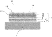
3・・・・ベース部材
5・・・・絶縁層
7・・・・接着層
9・・・・第1の接着層
11・・・第2の接着層
13・・・均熱板
15・・・フィラー
17・・・ヒータ電極
21・・・静電チャック
22・・・セラミック部材
23・・・吸着用電極
Claims (4)
- 上面が平面であるベース部材と、ヒータ電極が埋設されている絶縁層と、該絶縁層の上面に接着された上面がウエハ側となる均熱板と、前記ベース部材の上面に前記絶縁層の下面を接着している、フィラーを含む樹脂からなる接着層とを具備しており、該接着層は、前記ベース部材側の第1の接着層および前記絶縁層に接する第2の接着層の少なくとも2層を有し、前記第2の接着層が含むフィラーは平たい形状であり、該平たい形状のフィラーが前記第2の接着層の面方向に沿って平たく並んでおり、前記第2の接着層における前記フィラーの密度が前記第1の接着層における前記フィラーの密度よりも高いことを特徴とするウエハ加熱装置。
- 前記第2の接着層を平面視したときに前記平たい形状のフィラーの占める面積比率が前記第2の接着層の面積の50〜90%であることを特徴とする請求項1に記載のウエハ加熱装置。
- 前記平たい形状のフィラーが部分的に重なって並んでいることを特徴とする請求項1または請求項2に記載のウエハ加熱装置。
- 請求項1に記載のウエハ加熱装置と、前記均熱板の上面に接着された、吸着電極が埋設されており上面がウエハ載置面となるセラミック部材とを具備することを特徴とする静電チャック。
Priority Applications (1)
| Application Number | Priority Date | Filing Date | Title |
|---|---|---|---|
| JP2010540447A JP5116855B2 (ja) | 2008-11-25 | 2009-11-13 | ウエハ加熱装置、静電チャック |
Applications Claiming Priority (4)
| Application Number | Priority Date | Filing Date | Title |
|---|---|---|---|
| JP2008299080 | 2008-11-25 | ||
| JP2008299080 | 2008-11-25 | ||
| PCT/JP2009/069359 WO2010061740A1 (ja) | 2008-11-25 | 2009-11-13 | ウエハ加熱装置、静電チャックおよびウエハ加熱装置の製造方法 |
| JP2010540447A JP5116855B2 (ja) | 2008-11-25 | 2009-11-13 | ウエハ加熱装置、静電チャック |
Publications (2)
| Publication Number | Publication Date |
|---|---|
| JPWO2010061740A1 JPWO2010061740A1 (ja) | 2012-04-26 |
| JP5116855B2 true JP5116855B2 (ja) | 2013-01-09 |
Family
ID=42225618
Family Applications (1)
| Application Number | Title | Priority Date | Filing Date |
|---|---|---|---|
| JP2010540447A Active JP5116855B2 (ja) | 2008-11-25 | 2009-11-13 | ウエハ加熱装置、静電チャック |
Country Status (5)
| Country | Link |
|---|---|
| US (1) | US20110229837A1 (ja) |
| JP (1) | JP5116855B2 (ja) |
| KR (1) | KR101644495B1 (ja) |
| CN (1) | CN102217054B (ja) |
| WO (1) | WO2010061740A1 (ja) |
Cited By (2)
| Publication number | Priority date | Publication date | Assignee | Title |
|---|---|---|---|---|
| WO2016080262A1 (ja) * | 2014-11-20 | 2016-05-26 | 住友大阪セメント株式会社 | 静電チャック装置 |
| KR101791871B1 (ko) * | 2015-08-31 | 2017-10-31 | 세메스 주식회사 | 정전 척 및 이를 포함하는 기판 처리 장치 |
Families Citing this family (37)
| Publication number | Priority date | Publication date | Assignee | Title |
|---|---|---|---|---|
| JP5557164B2 (ja) * | 2010-03-24 | 2014-07-23 | Toto株式会社 | 静電チャック |
| AU2012301903B2 (en) | 2011-08-30 | 2015-07-09 | Watlow Electric Manufacturing Company | High definition heater system having a fluid medium |
| KR20130025025A (ko) * | 2011-09-01 | 2013-03-11 | 주식회사 코미코 | 정전척 |
| JP6017781B2 (ja) * | 2011-12-07 | 2016-11-02 | 新光電気工業株式会社 | 基板温調固定装置及びその製造方法 |
| US9224626B2 (en) * | 2012-07-03 | 2015-12-29 | Watlow Electric Manufacturing Company | Composite substrate for layered heaters |
| JP6165452B2 (ja) * | 2013-02-01 | 2017-07-19 | 株式会社日立ハイテクノロジーズ | プラズマ処理装置 |
| US9518946B2 (en) | 2013-12-04 | 2016-12-13 | Watlow Electric Manufacturing Company | Thermographic inspection system |
| JP6060889B2 (ja) * | 2013-12-16 | 2017-01-18 | 住友電気工業株式会社 | ウエハ加熱用ヒータユニット |
| DE102014008030A1 (de) * | 2014-05-28 | 2015-12-03 | Berliner Glas Kgaa Herbert Kubatz Gmbh & Co | Verfahren zur Herstellung einer elektrostatischen Haltevorrichtung |
| KR20160015510A (ko) * | 2014-07-30 | 2016-02-15 | 삼성전자주식회사 | 정전척 어셈블리, 이를 구비하는 반도체 제조장치, 및 이를 이용한 플라즈마 처리방법 |
| JP5948513B1 (ja) * | 2014-09-04 | 2016-07-06 | 日本碍子株式会社 | ウエハー保持台及びその製法 |
| JP6321522B2 (ja) * | 2014-11-05 | 2018-05-09 | 日本特殊陶業株式会社 | 加熱装置 |
| US10658222B2 (en) | 2015-01-16 | 2020-05-19 | Lam Research Corporation | Moveable edge coupling ring for edge process control during semiconductor wafer processing |
| JP6008063B1 (ja) * | 2015-03-24 | 2016-10-19 | 住友大阪セメント株式会社 | 静電チャック装置 |
| US9623679B1 (en) * | 2015-11-18 | 2017-04-18 | Xerox Corporation | Electrostatic platen for conductive pet film printing |
| JP6580975B2 (ja) * | 2015-12-18 | 2019-09-25 | 日本特殊陶業株式会社 | 静電チャックの製造方法 |
| JP2018101490A (ja) * | 2016-12-19 | 2018-06-28 | ニチコン株式会社 | ヒーターユニットおよびその製造方法 |
| JP6905399B2 (ja) * | 2017-06-23 | 2021-07-21 | 新光電気工業株式会社 | 基板固定装置 |
| US11837446B2 (en) | 2017-07-31 | 2023-12-05 | Lam Research Corporation | High power cable for heated components in RF environment |
| JP6616363B2 (ja) * | 2017-09-05 | 2019-12-04 | 日本特殊陶業株式会社 | 保持装置 |
| WO2019103722A1 (en) | 2017-11-21 | 2019-05-31 | Lam Research Corporation | Bottom and middle edge rings |
| US10761041B2 (en) | 2017-11-21 | 2020-09-01 | Watlow Electric Manufacturing Company | Multi-parallel sensor array system |
| JP6583897B1 (ja) * | 2018-05-25 | 2019-10-02 | ▲らん▼海精研股▲ふん▼有限公司 | セラミック製静電チャックの製造方法 |
| KR20250100800A (ko) * | 2018-05-31 | 2025-07-03 | 어플라이드 머티어리얼스, 인코포레이티드 | 극도의 균일성의 가열식 기판 지지 조립체 |
| CN118398464A (zh) | 2018-08-13 | 2024-07-26 | 朗姆研究公司 | 可更换和/或可折叠的用于等离子鞘调整的并入边缘环定位和定心功能的边缘环组件 |
| JP6899362B2 (ja) * | 2018-09-19 | 2021-07-07 | 日本特殊陶業株式会社 | 保持装置 |
| US11715652B2 (en) * | 2018-09-28 | 2023-08-01 | Ngk Insulators, Ltd. | Member for semiconductor manufacturing apparatus |
| KR102936833B1 (ko) * | 2019-03-01 | 2026-03-11 | 닛폰 하츠죠 가부시키가이샤 | 스테이지 및 스테이지 제작 방법 |
| JP7233289B2 (ja) * | 2019-04-11 | 2023-03-06 | 日本特殊陶業株式会社 | 保持装置の製造方法 |
| CN115315775A (zh) | 2020-03-23 | 2022-11-08 | 朗姆研究公司 | 衬底处理系统中的中环腐蚀补偿 |
| TWI828988B (zh) * | 2020-06-26 | 2024-01-11 | 日商日本特殊陶業股份有限公司 | 接合體及靜電夾頭 |
| CN116349002A (zh) | 2020-10-05 | 2023-06-27 | 朗姆研究公司 | 用于等离子体处理系统的可移动边缘环 |
| JP7458354B2 (ja) * | 2021-09-15 | 2024-03-29 | 日本特殊陶業株式会社 | 保持装置 |
| CN114388423B (zh) * | 2022-01-18 | 2025-02-18 | 浙江新纳陶瓷新材有限公司 | 一种静电吸盘的组装方法 |
| JP7509814B2 (ja) * | 2022-03-11 | 2024-07-02 | 日本特殊陶業株式会社 | 保持装置 |
| US20240266200A1 (en) * | 2023-02-08 | 2024-08-08 | Applied Materials, Inc. | Electrostatic Chuck |
| CN120236968A (zh) * | 2023-12-28 | 2025-07-01 | 中微半导体设备(上海)股份有限公司 | 一种用于晶圆处理装置的加热器及其制造方法和等离子处理装置 |
Citations (5)
| Publication number | Priority date | Publication date | Assignee | Title |
|---|---|---|---|---|
| JPH07335731A (ja) * | 1994-06-07 | 1995-12-22 | Fujitsu Ltd | 吸着装置およびその製造方法 |
| JP2001203257A (ja) * | 2000-01-20 | 2001-07-27 | Sumitomo Electric Ind Ltd | 半導体製造装置用ウェハ保持体 |
| JP2003273202A (ja) * | 2002-03-19 | 2003-09-26 | Ngk Insulators Ltd | 半導体支持装置 |
| JP2005277074A (ja) * | 2004-03-24 | 2005-10-06 | Kyocera Corp | ウェハ支持部材とその製造方法 |
| JP2006013302A (ja) * | 2004-06-29 | 2006-01-12 | Ngk Insulators Ltd | 基板載置装置及び基板温度調整方法 |
Family Cites Families (5)
| Publication number | Priority date | Publication date | Assignee | Title |
|---|---|---|---|---|
| JP2756075B2 (ja) * | 1993-08-06 | 1998-05-25 | 三菱電機株式会社 | 金属ベース基板およびそれを用いた電子機器 |
| TW492135B (en) * | 2000-05-25 | 2002-06-21 | Tomoegawa Paper Co Ltd | Adhesive sheets for static electricity chuck device, and static electricity chuck device |
| JP2003258065A (ja) * | 2002-02-27 | 2003-09-12 | Kyocera Corp | ウエハ載置ステージ |
| JP2005054157A (ja) * | 2003-08-07 | 2005-03-03 | Seiko Epson Corp | 導電性接着剤及びそれを用いて圧電素子を実装した圧電デバイス |
| JP4046120B2 (ja) * | 2005-01-27 | 2008-02-13 | 三菱電機株式会社 | 絶縁シートの製造方法およびパワーモジュールの製造方法 |
-
2009
- 2009-11-13 CN CN2009801454988A patent/CN102217054B/zh active Active
- 2009-11-13 WO PCT/JP2009/069359 patent/WO2010061740A1/ja not_active Ceased
- 2009-11-13 JP JP2010540447A patent/JP5116855B2/ja active Active
- 2009-11-13 US US13/131,014 patent/US20110229837A1/en not_active Abandoned
- 2009-11-13 KR KR1020117012816A patent/KR101644495B1/ko active Active
Patent Citations (5)
| Publication number | Priority date | Publication date | Assignee | Title |
|---|---|---|---|---|
| JPH07335731A (ja) * | 1994-06-07 | 1995-12-22 | Fujitsu Ltd | 吸着装置およびその製造方法 |
| JP2001203257A (ja) * | 2000-01-20 | 2001-07-27 | Sumitomo Electric Ind Ltd | 半導体製造装置用ウェハ保持体 |
| JP2003273202A (ja) * | 2002-03-19 | 2003-09-26 | Ngk Insulators Ltd | 半導体支持装置 |
| JP2005277074A (ja) * | 2004-03-24 | 2005-10-06 | Kyocera Corp | ウェハ支持部材とその製造方法 |
| JP2006013302A (ja) * | 2004-06-29 | 2006-01-12 | Ngk Insulators Ltd | 基板載置装置及び基板温度調整方法 |
Cited By (4)
| Publication number | Priority date | Publication date | Assignee | Title |
|---|---|---|---|---|
| WO2016080262A1 (ja) * | 2014-11-20 | 2016-05-26 | 住友大阪セメント株式会社 | 静電チャック装置 |
| JPWO2016080262A1 (ja) * | 2014-11-20 | 2017-04-27 | 住友大阪セメント株式会社 | 静電チャック装置 |
| US10079167B2 (en) | 2014-11-20 | 2018-09-18 | Sumitomo Osaka Cement Co., Ltd. | Electrostatic chucking device |
| KR101791871B1 (ko) * | 2015-08-31 | 2017-10-31 | 세메스 주식회사 | 정전 척 및 이를 포함하는 기판 처리 장치 |
Also Published As
| Publication number | Publication date |
|---|---|
| CN102217054A (zh) | 2011-10-12 |
| CN102217054B (zh) | 2013-05-08 |
| WO2010061740A1 (ja) | 2010-06-03 |
| KR101644495B1 (ko) | 2016-08-01 |
| KR20110089336A (ko) | 2011-08-05 |
| US20110229837A1 (en) | 2011-09-22 |
| JPWO2010061740A1 (ja) | 2012-04-26 |
Similar Documents
| Publication | Publication Date | Title |
|---|---|---|
| JP5116855B2 (ja) | ウエハ加熱装置、静電チャック | |
| JP5421402B2 (ja) | ウェハ支持部材 | |
| JP4349952B2 (ja) | ウェハ支持部材とその製造方法 | |
| CN103443914B (zh) | 静电卡盘装置 | |
| JP4749072B2 (ja) | ウェハ保持体 | |
| JP6224171B2 (ja) | 半導体モジュールの製造方法 | |
| JP6008063B1 (ja) | 静電チャック装置 | |
| JP7060084B2 (ja) | 絶縁回路基板用接合体の製造方法および絶縁回路基板用接合体 | |
| CN115734994B (zh) | 粘合剂转移膜及使用粘合剂转移膜制造电源模块基板的方法 | |
| JP2005159018A (ja) | ウェハ支持部材 | |
| JP6572788B2 (ja) | 静電チャック装置 | |
| JP6597437B2 (ja) | 静電チャック装置 | |
| JP5343802B2 (ja) | 静電チャック装置 | |
| JP4614868B2 (ja) | 接合体及びその製造方法 | |
| JP7344759B2 (ja) | 静電チャック装置 | |
| JP2010277809A (ja) | 加熱ヒータおよびそれを備えた装置 | |
| JP2022094466A (ja) | 静電チャック装置 | |
| JP6853443B2 (ja) | パワーモジュール用基板の製造方法 | |
| JP6642170B2 (ja) | 静電チャック装置及びその製造方法 | |
| JP4936877B2 (ja) | 接合体とこれを用いたウェハ支持部材及びウェハの処理方法 | |
| JP2017157607A (ja) | 静電チャック装置 | |
| JP2023044754A (ja) | 接合体の製造方法及び絶縁回路基板の製造方法 | |
| JP2023044755A (ja) | 接合体の製造方法及び絶縁回路基板の製造方法 |
Legal Events
| Date | Code | Title | Description |
|---|---|---|---|
| A131 | Notification of reasons for refusal |
Free format text: JAPANESE INTERMEDIATE CODE: A131 Effective date: 20120313 |
|
| A521 | Request for written amendment filed |
Free format text: JAPANESE INTERMEDIATE CODE: A523 Effective date: 20120507 |
|
| A131 | Notification of reasons for refusal |
Free format text: JAPANESE INTERMEDIATE CODE: A131 Effective date: 20120710 |
|
| A521 | Request for written amendment filed |
Free format text: JAPANESE INTERMEDIATE CODE: A523 Effective date: 20120824 |
|
| TRDD | Decision of grant or rejection written | ||
| A01 | Written decision to grant a patent or to grant a registration (utility model) |
Free format text: JAPANESE INTERMEDIATE CODE: A01 Effective date: 20120918 |
|
| A01 | Written decision to grant a patent or to grant a registration (utility model) |
Free format text: JAPANESE INTERMEDIATE CODE: A01 |
|
| A61 | First payment of annual fees (during grant procedure) |
Free format text: JAPANESE INTERMEDIATE CODE: A61 Effective date: 20121016 |
|
| R150 | Certificate of patent or registration of utility model |
Ref document number: 5116855 Country of ref document: JP Free format text: JAPANESE INTERMEDIATE CODE: R150 Free format text: JAPANESE INTERMEDIATE CODE: R150 |
|
| FPAY | Renewal fee payment (event date is renewal date of database) |
Free format text: PAYMENT UNTIL: 20151026 Year of fee payment: 3 |