JP5117082B2 - Light modulator - Google Patents
Light modulator Download PDFInfo
- Publication number
- JP5117082B2 JP5117082B2 JP2007058796A JP2007058796A JP5117082B2 JP 5117082 B2 JP5117082 B2 JP 5117082B2 JP 2007058796 A JP2007058796 A JP 2007058796A JP 2007058796 A JP2007058796 A JP 2007058796A JP 5117082 B2 JP5117082 B2 JP 5117082B2
- Authority
- JP
- Japan
- Prior art keywords
- optical
- curvature
- optical waveguide
- interaction
- optical modulator
- Prior art date
- Legal status (The legal status is an assumption and is not a legal conclusion. Google has not performed a legal analysis and makes no representation as to the accuracy of the status listed.)
- Expired - Fee Related
Links
- 230000003287 optical effect Effects 0.000 claims description 213
- 230000003993 interaction Effects 0.000 claims description 84
- 239000000758 substrate Substances 0.000 claims description 35
- 230000002452 interceptive effect Effects 0.000 claims description 26
- 230000008859 change Effects 0.000 claims description 4
- 239000004020 conductor Substances 0.000 description 36
- 229910004298 SiO 2 Inorganic materials 0.000 description 9
- 230000000694 effects Effects 0.000 description 8
- 230000001902 propagating effect Effects 0.000 description 8
- 238000000034 method Methods 0.000 description 6
- 238000003780 insertion Methods 0.000 description 5
- 230000037431 insertion Effects 0.000 description 5
- 230000008901 benefit Effects 0.000 description 4
- 238000004891 communication Methods 0.000 description 4
- 238000007796 conventional method Methods 0.000 description 3
- 230000005684 electric field Effects 0.000 description 3
- GQYHUHYESMUTHG-UHFFFAOYSA-N lithium niobate Chemical compound [Li+].[O-][Nb](=O)=O GQYHUHYESMUTHG-UHFFFAOYSA-N 0.000 description 3
- 229910052751 metal Inorganic materials 0.000 description 3
- 239000002184 metal Substances 0.000 description 3
- 230000015572 biosynthetic process Effects 0.000 description 2
- 239000012212 insulator Substances 0.000 description 2
- 230000005693 optoelectronics Effects 0.000 description 2
- 239000010453 quartz Substances 0.000 description 2
- 230000005855 radiation Effects 0.000 description 2
- 239000004065 semiconductor Substances 0.000 description 2
- VYPSYNLAJGMNEJ-UHFFFAOYSA-N silicon dioxide Inorganic materials O=[Si]=O VYPSYNLAJGMNEJ-UHFFFAOYSA-N 0.000 description 2
- WSMQKESQZFQMFW-UHFFFAOYSA-N 5-methyl-pyrazole-3-carboxylic acid Chemical compound CC1=CC(C(O)=O)=NN1 WSMQKESQZFQMFW-UHFFFAOYSA-N 0.000 description 1
- 229910018072 Al 2 O 3 Inorganic materials 0.000 description 1
- 229910013641 LiNbO 3 Inorganic materials 0.000 description 1
- 238000010521 absorption reaction Methods 0.000 description 1
- 238000013459 approach Methods 0.000 description 1
- 238000013461 design Methods 0.000 description 1
- 238000011161 development Methods 0.000 description 1
- 239000003989 dielectric material Substances 0.000 description 1
- 238000009792 diffusion process Methods 0.000 description 1
- 230000007613 environmental effect Effects 0.000 description 1
- 238000005530 etching Methods 0.000 description 1
- 230000006872 improvement Effects 0.000 description 1
- 238000010348 incorporation Methods 0.000 description 1
- 239000000463 material Substances 0.000 description 1
- 239000000203 mixture Substances 0.000 description 1
- 238000012544 monitoring process Methods 0.000 description 1
- 230000009467 reduction Effects 0.000 description 1
- 230000003068 static effect Effects 0.000 description 1
Images


Landscapes
- Optical Modulation, Optical Deflection, Nonlinear Optics, Optical Demodulation, Optical Logic Elements (AREA)
Description
本発明は電気光学効果や熱光学効果を利用して、光導波路に入射した光を変調して光信号パルスとして出射する光変調器に関する。 The present invention utilizes an electro-optical effect or thermal optical effect relates to an optical modulator for emitting an optical signal pulse by modulating light incident on the optical waveguide.
代表的な光変調デバイスとして誘電体材料を用いた光変調器がある。近年、高速、大容量の光通信システムが実用化されているが、このような高速、大容量の光通信システムに組込むための高速、小型、かつ低価格の光変調器の開発が求められている。 There is an optical modulator using a dielectric material as a typical optical modulation device. In recent years, high-speed and large-capacity optical communication systems have been put into practical use, and development of high-speed, small, and low-cost optical modulators for incorporation into such high-speed and large-capacity optical communication systems is required. Yes.
このような要望に応える光変調器として、リチウムナイオベート(LiNbO3)のように電界を印加することにより屈折率が変化する、いわゆる電気光学効果を有する基板(以下、LN基板と略す)に光導波路と進行波電極を形成した進行波電極型リチウムナイオベート光変調器(以下、LN光変調器と略す)がある。このLN光変調器は、その優れたチャーピング特性から2.5Gbit/s、10Gbit/sの大容量光通信システムに適用されている。最近はさらに40Gbit/sの超大容量光通信システムにも適用が検討されている。 As an optical modulator that meets such demands, a light modulator such as lithium niobate (LiNbO 3 ) is used for a substrate having a so-called electro-optical effect (hereinafter abbreviated as an LN substrate) whose refractive index changes by applying an electric field. There is a traveling wave electrode type lithium niobate optical modulator (hereinafter abbreviated as an LN optical modulator) in which a waveguide and a traveling wave electrode are formed. This LN optical modulator is applied to a large capacity optical communication system of 2.5 Gbit / s and 10 Gbit / s because of its excellent chirping characteristics. Recently, application to a 40 Gbit / s ultra-high capacity optical communication system is also being studied.
以下、従来、実用化され、又は提唱されてきたリチウムナイオベートの電気光学効果を利用した各LN光変調器の特徴を順番に説明していく。 Hereinafter, the characteristics of each LN optical modulator using the electro-optic effect of lithium niobate, which has been practically used or proposed, will be described in order.
(第1の従来技術)
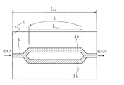
図9は、z−カットLN基板を用いて構成した特許文献1に開示された第1の従来技術のLN光変調器についての斜視図であり、図10は図9のA−A'線における断面図である。
(First prior art)
FIG. 9 is a perspective view of the first prior art LN optical modulator disclosed in
z−カットLN基板1上に光導波路3が形成されている。この光導波路3は、金属Tiを1050℃で約10時間熱拡散して形成した光導波路であり、マッハツェンダ干渉系(あるいは、マッハツェンダ光導波路)を構成している。従って、図9の中にIとして示した光導波路3の高周波電気信号(あるいは、RF電気信号)と光が相互作用する領域(相互作用領域、あるいは相互作用部と言う)には2本の相互作用光導波路3a、3b、つまりマッハツェンダ光導波路の2本のアームが形成されている。
An
この光導波路3の上面にSiO2バッファ層2が形成され、このSiO2バッファ層2の上面に進行波電極4が形成されている。進行波電極4としては、1つの中心導体4aと2つの接地導体4b、4cを有するコプレーナウェーブガイド(CPW)を用いている。なお、通常、進行波電極4はAuにより形成されている。5はz−カットLN基板1を用いて製作したLN変調器に特有の焦電効果に起因する温度ドリフトを抑圧するための導電層であり、通常はSi導電層を用いる。なお、説明の簡単のために、図10においては図9には図示したSi導電層5を省略している。
An SiO 2 buffer layer 2 is formed on the upper surface of the
変調用の高周波(RF)電気信号をこの光変調器の高周波電気信号給電線6を介して中心導体4aと接地導体4bに供給すると、中心導体4aと接地導体4bの間に電界が印加される。z−カットLN基板1は電気光学効果を有するので、この電界により屈折率変化を生じ、2本の相互作用光導波路3a、3bを伝搬する光の位相にずれが発生する。このずれがπになった場合、光導波路3のマッハツェンダ光導波路としての合波部において、高次モードを励振し、光はOFF状態になる。なお、7は高周波電気信号出力線であり、終端抵抗で置き換えても良い。
When a high frequency (RF) electric signal for modulation is supplied to the
図10からわかるように、図9に示した特許文献1の光変調器の特徴としては、1)中心導体4aの幅Sを相互作用光導波路3a、3bの幅とほぼ同じ6μm〜12μm程度としている、2)中心導体4aと接地導体4b、4c間のギャップWを15〜30μmと広くしている、さらに3)相互作用光導波路3a、3bを伝搬する光の中心導体4aと接地導体4b、4cからなる進行波電極4を構成する金属による吸収を抑えるためにのみ使用されてきたSiO2バッファ層2の比誘電率が4〜6と比較的低いことを利用して、SiO2バッファ層2の厚みDを400nm〜1.5μm程度と厚くすることにより、高周波電気信号のマイクロ波等価屈折率nmを低減して、相互作用光導波路3a、3bを導波する光の等価屈折率noに近づけるとともに、特性インピーダンスをなるべく50Ωに近づけている。また、図10に示した第1の従来技術では、特許文献2に開示された進行波電極4の厚みTを厚くすることによりマイクロ波等価屈折率nmをよりいっそう低減して、光の等価屈折率noに近づけている。
As can be seen from FIG. 10, the characteristics of the optical modulator of
こうした構造をとることにより、中心導体4aの幅Sが30μm程度、中心導体4aと接地導体4b、4c間のギャップWが6μm程度、SiO2バッファ層2の厚みDが300nm程度であったそれまでの構造と比べて、光変調帯域、特性インピーダンスなど光変調器としての特性が大幅に改善できた。しかしながら、光変調帯域、駆動電圧、特性インピーダンスなどについてさらに改善された特性が必要となり、次に述べる第2の従来技術として、いわゆるリッジ構造が提案された。
By adopting such a structure, the width S of the
(第2の従来技術)
第1の従来技術をさらに高性能化するために特許文献3、特許文献4に提案されたリッジ構造を第2の従来技術として図11、図12に示す。ここで、8aは中心導体4aの下のリッジ、8bは接地導体4bの下のリッジ、8cは接地導体4cの下のリッジ、9はSiO2バッファ層である。10aはリッジ8a、8b間の空隙、10bはリッジ8a、8c間の空隙である。
(Second prior art)
FIG. 11 and FIG. 12 show the ridge structure proposed in
また、図12において11a、11bは中心導体4aから出て接地導体4b、4cに入る電気力線であり、相互作用光導波路3a、3bに作用してそれらの屈折率を変化させる(あるいは、相互作用光導波路3a、3bを伝搬する光と相互作用するとも言える)。
In FIG. 12,
この第2の従来技術ではz−カットLN基板1に8aや8bなどのリッジが形成されているため、電気力線11aはリッジ8a、8b間の空隙10aを電気力線11bはリッジ8a、8c間の空隙10bを感じる。その結果、高周波電気信号のマイクロ波等価屈折率nmがより低減して、相互作用光導波路3a、3bを導波する光の等価屈折率noに近づく、あるいは特性インピーダンスが50Ωに向かって高くなるという利点がある。さらに、電気力線11a、11bには比誘電率が高い領域に閉じこもる性質があるので、相互作用光導波路3a、3bを伝搬する光との相互作用の効率が高くなり、結果的に駆動電圧を低減できる。通常、リッジ8a、8b、8cの高さHとしては2〜5μm程度、進行波電極の厚みTとしては6〜18μm程度、SiO2バッファ層2の厚みとしては400nm〜1.5μm程度が使用される。
In the second prior art, ridges such as 8a and 8b are formed on the z-
この第2の従来技術により、光変調帯域、駆動電圧、特性インピーダンスなど、光変調器としての基本性能について図10に示した第1の従来技術よりも大幅に改善された特性が実現できた。 With this second conventional technique, characteristics such as an optical modulation band, drive voltage, characteristic impedance, etc., which are significantly improved as compared with the first conventional technique shown in FIG.
しかしながら、この第2の従来技術でもまだ改善すべき余地がある。次にこの点について図13、図14を用いて議論する。高周波における駆動電圧などLN光変調器の重要な特性は高周波電気信号と相互作用光導波路3a、3bを伝搬する光が相互作用する相互作用部Iの長さLintに強く依存する。そして、この相互作用部Iの長さLintはz−カットLN基板1の長さLLNにより決定される。
However, there is still room for improvement in the second prior art. Next, this point will be discussed with reference to FIGS. The important characteristics of the LN optical modulator, such as the driving voltage at high frequency, strongly depend on the length L int of the interaction part I where the high-frequency electrical signal interacts with the light propagating through the interaction
図14には性能を評価する極めて簡単な目安として、相互作用部Iの長さLintに対するVπ(静的な電圧における半波長電圧)を示す。図からわかるように、相互作用部Iの長さLintが長いほどVπは低くなり、性能的に有利になると言える。このVπと相互作用部Iの長さ(相互作用光導波路の長さ、あるいは相互作用長という)LintはよくVπ・Lintとして議論されるように性能指数として重要であり、相互作用長Lintは長いほど駆動電圧を低減するためにも、また設計の自由度を増すためにも有利となる。 FIG. 14 shows Vπ (half-wave voltage at a static voltage) with respect to the length L int of the interaction part I as a very simple guideline for evaluating the performance. As can be seen from the figure, it can be said that the longer the length L int of the interaction part I, the lower Vπ, which is advantageous in terms of performance. This Vπ and the length of the interaction part I (the length of the interaction optical waveguide or the interaction length) L int is important as a figure of merit as often discussed as Vπ · L int , and the interaction length L A longer int is advantageous for reducing the drive voltage and increasing the degree of freedom in design.
これまでのLN光変調器では相互作用部Iの長さLintがパッケージの大きさやウェーハの大きさから制限を受けるため、約20mmから高々40mmと短く、この短い相互作用長がLN光変調器の性能を制限していたと言っても過言ではない。
以上のように、光変調帯域、駆動電圧、特性インピーダンスなどの光変調器としての特性を大幅に改善できた第2の従来技術による光変調器もLN基板の長さによりその相互作用長が制限され、その結果、高周波駆動電圧、特性インピーダンスなどの光変調器としての基本特性が決まっていた。換言すると、LN基板の長さが光変調器の特性を決定していたと言える。 As described above, the optical modulator according to the second prior art which can greatly improve the characteristics as the optical modulator such as the optical modulation band, the driving voltage, and the characteristic impedance is also limited in the interaction length by the length of the LN substrate. As a result, basic characteristics as an optical modulator such as a high-frequency driving voltage and characteristic impedance have been determined. In other words, it can be said that the length of the LN substrate determines the characteristics of the optical modulator.
本発明はこのような事情に鑑みてなされたものであり、小型で、駆動電圧が低く、光変調帯域が広く、特性インピーダンスについて大幅に改善された光変調器を提供することを目的とする。 The present invention has been made in view of such circumstances, and an object of the present invention is to provide an optical modulator that is small in size, has a low driving voltage, has a wide optical modulation band, and is greatly improved in characteristic impedance.
上記課題を解決するために、本発明の請求項1の光変調器は、基板と該基板に形成された光導波路と、高周波電気信号を印加するための電極とを備え、該光導波路は、該電極に高周波電気信号を印加することにより屈折率が変化する2本の相互作用光導波路と、変調された光が出力される出力用光導波路とを含むマッハツェンダ光導波路を構成する光変調器において、前記2本の相互作用光導波路は、ターン数が1回以上の渦巻状に構成されるとともに、少なくとも2つの曲率半径の異なる曲線を挟んで配置されており、最も大きな曲率半径を有する曲線の曲率中心を中心とする円を描いた場合に、該円の中に最も小さな曲率半径を有する曲線の曲率中心が含まれていることを特徴とする。
本発明の請求項2の光変調器は、基板と該基板に形成された光導波路と、高周波電気信号を印加するための電極とを備え、該光導波路は、該電極に高周波電気信号を印加することにより屈折率が変化する2本の相互作用光導波路と、変調された光が出力される出力用光導波路とを含むマッハツェンダ光導波路を構成する光変調器において、前記2本の相互作用光導波路は、少なくとも2つの曲率半径の異なる曲線を挟んで配置されており、最も大きな曲率半径を有する曲線の曲率中心を中心とする円を描いた場合に、該円の中に最も小さな曲率半径を有する曲線の曲率中心が含まれており、前記2本の相互作用光導波路のパターンが、前記2本の相互作用光導波路についてのパターンの全体の配置の中心に対して点対称であることを特徴とする。
In order to solve the above problems, an optical modulator according to
An optical modulator according to
本発明の請求項3の光変調器は、前記2本の相互作用光導波路の屈折率が変化する部分の長さが互いに等しいことを特徴とする。
The optical modulator according to
本発明の請求項4の光変調器は、前記2本の相互作用光導波路が互いに交差していることを特徴とする。
The optical modulator according to
本発明の請求項5の光変調器は、前記2本の相互作用光導波路が互いに交差せず配置されていることを特徴とする。
The optical modulator according to
本発明の請求項6の光変調器は、前記出力用光導波路が前記2本の相互作用光導波路と交差していることを特徴とする。
The optical modulator according to
本発明の請求項7の光変調器は、前記出力用光導波路が前記2本の相互作用光導波路と交差しないように配置されていることを特徴とする。
The optical modulator according to
本発明の請求項8の光変調器は、前記2本の相互作用光導波路の少なくとも一部がリッジ構造であることを特徴とする。 An optical modulator according to an eighth aspect of the present invention is characterized in that at least a part of the two interactive optical waveguides has a ridge structure.
本発明の請求項9の光変調器は、前記2本の相互作用光導波路の近傍の少なくとも一箇所の基板が薄くなっていることを特徴とする。
The optical modulator according to
本発明では、電圧を印加することにより屈折率が変化する相互作用光導波路を曲線形状により構成するので、従来にない極めて小さなチップサイズでも相互作用長を任意に設定できるばかりでなく、極めて長くすることも可能となり、光変調デバイスのモジュールとして大幅な小型化を達成できる。そして相互作用長が長くなれば駆動電圧を低減できるばかりでなく、バッファ層を厚く設定できるので、容易に高周波電気信号と光との速度を整合(速度整合)することできる、特性インピーダンスを50Ωに近くできる、あるいは高周波電気信号の伝搬損失を小さくできるなどの利点が生じる。さらに、中心導体14aと接地導体14b、14cとのギャップも広く設定できるので、特性インピーダンスをさらに50Ωに近くすることが可能となる、また高周波電気信号の伝搬損失もさらに小さくできる。以上のように本発明を適用して相互作用長を長くした結果、光変調器の性能が著しく向上し、低い駆動電圧で高速な光変調が可能となる。あるいは熱光学効果を用いた場合には、極めて少ない発熱量で高効率な光変調が可能となる。
In the present invention, the interaction optical waveguide whose refractive index is changed by applying a voltage is configured by a curved shape, so that the interaction length can be arbitrarily set even with an extremely small chip size which has not been conventionally achieved, and is also made extremely long. It is also possible to achieve a significant reduction in size as a module of an optical modulation device. And if the interaction length is longer, not only can the drive voltage be reduced, but also the buffer layer can be set thick, so that the speed of the high-frequency electrical signal and light can be easily matched (speed matching), and the characteristic impedance is 50Ω. There are advantages such as being close to each other or reducing the propagation loss of the high-frequency electrical signal. Furthermore, since the gap between the
以下、本発明の実施形態について説明するが、図9から図13に示した従来技術と同一の符号は同一機能部に対応しているため、ここでは同一の符号を持つ機能部の説明を省略する。 Hereinafter, embodiments of the present invention will be described. However, since the same reference numerals as those in the related art shown in FIGS. 9 to 13 correspond to the same functional units, description of the functional units having the same reference numerals is omitted here. To do.
(第1の実施形態)
図1に本発明における第1の実施形態の光導波路13を示す。13a、13bは高周波電気信号と光導波路を伝搬する光が相互作用するリッジ構造の相互作用光導波路であり、図1においてz−カットLN基板1の四隅を曲線で、また各辺に対向して直線としてもよいが、説明の簡単のために大部分が曲線により形成されているとする。また、VIIは光導波路3の分岐部、VIIIは光導波路の合波部、13cは出力用光導波路である。なお、相互作用光導波路13a、13bの形状は例えば螺旋や楕円など、円弧以外の曲線でも良いが、ここでは説明を簡単にするために円弧とする。
(First embodiment)
FIG. 1 shows an
ここで、相互作用領域IIでは相互作用光導波路13a、13bが各々半径R1の円の内側と外側に位置している。その結果、相互作用領域IIでは相互作用光導波路13bの方が相互作用光導波路13aよりも長い。そして光導波路の交差部IIIを設けているので、相互作用領域IVでは相互作用光導波路13b、13aが各々曲率半径R2の円の内側と外側に位置している。つまり、領域IVでは相互作用光導波路13aの方が相互作用光導波路13bよりも長くなる。
Here, the interaction region II, the interaction
このように外側の円弧の方が内側の円弧よりも長くなるので、本実施形態では光導波路の交差部IIIを設けることにより、光導波路3の分岐部VIIから合波部VIIIにいたるまでに相互作用光導波路13a、13bの全体としての長さが等しくなるように工夫している。
Since the outer arc is longer than the inner arc in this way, in the present embodiment, by providing the intersection portion III of the optical waveguide, it is possible to reach each other from the branching portion VII to the multiplexing portion VIII of the
相互作用光導波路13a、13bの長さが全体として互いに異なると波長を変えた際に挿入損失が変動する、あるいはこのことと等価であるが、環境温度が変化した場合にも相互作用光導波路13a、13bの光学的な長さの差が変化することになり、やはり挿入損失が変動してしまう。これを避けるために、本実施形態では光導波路の交差部IIIを導入することにより相互作用光導波路13a、13bの光学的な長さを同じにした。そして、図1に示す本発明の第1の実施形態では出力用光導波路13cが相互作用光導波路13a、13bと交差している。
If the lengths of the interaction
また、相互作用領域IIと相互作用領域IVの円弧の中心を各々VとVIとすると、中心Vと中心VIとは一致していても良いし、一致していなくても良い。但し、本発明では、中心を相互作用領域IIの曲線の中心Vとして大きな方の曲率半径R1で全周を描いた円の中に相互作用領域IVの曲線の中心VIが入るように規定している。こうすることにより全体の寸法を小さくすることが可能となる。 Further, if the centers of the arcs of the interaction region II and the interaction region IV are V and VI, respectively, the center V and the center VI may or may not coincide with each other. However, the present invention defines as a center VI curve of the interaction region IV falls within the circle drawn the entire circumference with a radius of curvature R 1 of the larger center as the center V curve of the interaction region II ing. In this way, the overall dimensions can be reduced.
なお、螺旋や円弧以外の曲線のように相互作用光導波路13a、13bの位置とともに、曲率が変わる場合には一部の曲線の曲率半径、あるいは曲線の中心を用いて考えれば良い。また、ここで曲線の中心とはその曲率半径により描いた円弧(もしくは、円)の回転中心を意味している。
When the curvature changes with the position of the interaction
図2では進行波電極14に着目して示している。ここで、14aは中心導体、14b、14cは接地導体である。この図からわかるように、相互作用領域II、光導波路の交差部III、及び相互作用領域IVにわたって、中心導体14aが相互作用光導波路13bの上に形成されている。
In FIG. 2, the traveling
次に、本実施形態により実現することのできる利点について考察する。相互作用領域IIと相互作用領域IVとの間にある接地導体14bの幅(図2中にGWと表記)は、中心導体14aと接地導体14bとのギャップ(15〜30μm)のたかだか数倍と小さいので、相互作用領域IIにおける円弧の曲率半径R1と相互作用領域IVにおける円弧の曲率半径R2とはほぼ等しい(つまり、R1≒R2と近似できる)。つまり、曲率半径R1や曲率半径R2により形成される相互作用領域が例えば360度の円から成っている場合、その長さ(相互作用長)はほぼ2πR1と考えてよい。
Next, advantages that can be realized by this embodiment will be considered. The width of the
図3には曲率半径R1が4mmの場合における相互作用長の全長Ltotalと円のターン数との関係を示す。なお、図中には図9や図13に示した従来技術での相互作用長の範囲(20〜40mm)も示している。図からわかるように、本実施形態のように円の曲率半径R1を4mmと小さくしても、1ターンで25.1mmの相互作用長となるので、本実施形態では従来技術の相互作用長はわずか0.8〜1.6ターンで実現できる。 FIG. 3 shows the relationship between the total length L total of the interaction length and the number of turns of the circle when the curvature radius R 1 is 4 mm. In addition, the range (20-40 mm) of the interaction length in the prior art shown in FIG. 9 and FIG. 13 is also shown in the figure. As can be seen, even if the radius of curvature R 1 of a circle as in the present embodiment is as small as 4 mm, since the interaction length of 25.1mm in one turn, the interaction length of the prior art in this embodiment Can be realized with only 0.8 to 1.6 turns.
よって、相互作用光導波路13a、13bが構成する円弧(あるいは、曲線)の中心角は250度以上、さらには図1のように360度以上、さらには多重のターンとすることが望ましい。そうすることによりLN光変調器のチップのサイズを大きくすることなく、相互作用長を自由に設定できるとともに、相互作用長の長さを著しく長くすることも可能となる。その結果、本発明の効果を著しく発揮できる。
Therefore, it is desirable that the central angle of the arc (or curve) formed by the interactive
つまり、前述のように円を多重のターンとしても各々の円の半径はほとんど変わらないので、極めて長い相互作用長を容易に実現できる。例えば5ターンとすることにより120mmもの長さの相互作用長を得ることが可能となる。この場合も円の曲率半径R1は4mmと小さいので、光変調器のチップのサイズも8.5mmx8.5mm、あるいは9mmx9mm程度と小さくて良い。 In other words, as described above, even if a circle is made into multiple turns, the radius of each circle hardly changes, so that an extremely long interaction length can be easily realized. For example, an interaction length as long as 120 mm can be obtained by setting 5 turns. In this case the radius of curvature R 1 of the circle also are 4mm and small size of the chip of the optical modulator may be 8.5mmx8.5mm or as small as about 9Mmx9mm,.
従来技術による光変調器のチップを用いて光変調器モジュールを製作するとその幅は12〜14mm強で長さは75〜100mm程度であった。従って、本発明の光変調器のチップを用いて光変調器モジュールを製作すると、従来技術による光変調器モジュールと幅はほぼ同じで、長さは12〜15mm程度と短くなり、従来技術による変調器のモジュールの長さと比較して約1/5〜1/7と大幅な小型化を図ることが可能となる。 When an optical modulator module is manufactured using a chip of an optical modulator according to the prior art, the width is slightly over 12 to 14 mm and the length is about 75 to 100 mm. Accordingly, when an optical modulator module is manufactured using the optical modulator chip of the present invention, the width is almost the same as the conventional optical modulator module and the length is as short as about 12 to 15 mm. As compared with the length of the module of the vessel, it becomes possible to achieve a significant downsizing of about 1/5 to 1/7.
さらに図3で説明したように、相互作用長が長くなれば駆動電圧に対して有利となるのでバッファ層を厚く設定できる。従って、容易に高周波電気信号と光との速度を整合(速度整合)することできる、特性インピーダンスを50Ωに近くできる、あるいは高周波電気信号の伝搬損失を小さくできるなどの利点が生じる。その上、中心導体14aと接地導体14b、14cとのギャップも広く設定できるので、特性インピーダンスをさらに50Ωに近くすることが可能となる、また高周波電気信号の伝搬損失もさらに小さくできる。
Further, as described with reference to FIG. 3, if the interaction length is longer, it is advantageous for the driving voltage, so that the buffer layer can be set thick. Therefore, there are advantages that the speed of the high-frequency electric signal and the light can be easily matched (speed matching), the characteristic impedance can be close to 50Ω, or the propagation loss of the high-frequency electric signal can be reduced. In addition, since the gap between the
以上の結果、光変調器の性能が著しく向上し、低い駆動電圧で高速な光変調が可能となる。なお、交差部IIIのように光導波路同士が交差する箇所において生じる挿入損失の増加は0.2dB、あるいはそれ以下であるので大きな問題とはならない。 As a result, the performance of the optical modulator is remarkably improved, and high-speed optical modulation is possible with a low driving voltage. It should be noted that the increase in insertion loss that occurs at the location where the optical waveguides intersect like the intersection III is 0.2 dB or less, which is not a big problem.
なお、以上の説明においては、円弧の曲率の半径は4mmとして説明したが、これは一例であってそれ以上でも良いし、逆に2mmあるいは3mm程度でも良い。そして、チップサイズはわずか4mmx4mm、あるいは6mmx6mm程度と小さいにもかかわらず従来にない高性能なLN光変調器を実現できる。 In the above description, the radius of curvature of the arc has been described as 4 mm. However, this is only an example and may be more than that, or conversely, may be about 2 mm or 3 mm. And although the chip size is as small as 4 mm × 4 mm or 6 mm × 6 mm, an unprecedented high-performance LN optical modulator can be realized.
(第2の実施形態)
図4に本発明の第2の実施形態を示す。本実施形態では図1に示した第1の実施形態における光導波路の交差部III、即ち相互作用光導波路13a、13bの長さを同じにするために設けた光導波路の交差部は存在しない。前述のように、円の外側の相互作用光導波路13bは円の内側の相互作用光導波路13aよりも長くなる。そこで、進行波電極14を主眼として示した図5からわかるように、領域IXにおいて中心導体14aから出てくる電気力線が相互作用光導波路13bに作用しないように、中心導体14aを相互作用光導波路13bの直上からずらして配置している。これにより高周波電気信号と光が相互作用する長さを相互作用光導波路13aと13bにおいて等しくしている。こうすることにより、LN光変調器としての適切なチャープ特性を確保できる。
(Second Embodiment)
FIG. 4 shows a second embodiment of the present invention. In the present embodiment, there is no crossing portion of the optical waveguide provided in order to make the lengths of the intersections III of the optical waveguides, that is, the interaction
(第3の実施形態)
図6には本発明の第3の実施形態を示す。この実施形態では、相互作用領域IVの曲線の中心VIと相互作用領域IIの曲線の中心Vは一致しており、相互作用光導波路13a、13bの全体のパターンはこの曲線の中心VIとVに対して点対称な構造となっている。
(Third embodiment)
FIG. 6 shows a third embodiment of the present invention. In this embodiment, the center VI of the curve of the interaction region IV and the center V of the curve of the interaction region II coincide with each other, and the entire pattern of the interaction
こうすることにより、相互作用領域IIと相互作用領域IVにおける円弧の曲率半径R1と相互作用領域IVにおける円弧の曲率半径R2が等しくなり(R1=R2)、その結果、相互作用光導波路13a、13bの長さが等しくなる。
By doing so, the radius of curvature R 1 of the arc in the interaction region II and the interaction region IV is equal to the radius of curvature R 2 of the arc in the interaction region IV (R 1 = R 2 ). The lengths of the
そして、相互作用光導波路13a、13bは互いに交差することはないので、光の挿入損失が最も低くなる。
Since the interaction
また、この実施形態でも相互作用領域IVの曲線の中心VIは曲率半径R1で全周を描いた円の中に入っている、あるいは相互作用光導波路13a、13bで形づくられている曲線のうち、最小の曲率半径からなる曲線の円周上の中心X、XIの外側に、さらに曲線からなる相互作用光導波路13a、13bが存在するなどの本発明の特徴を有している。
The center VI curve of the interaction region IV in this embodiment of the curve being shaped by the radius of curvature R 1 at is contained within a circle depicting the entire circumference or the interaction
なお、本発明の全ての実施形態について言えることであるが、出力光導波路13cは相互作用光導波路13a、13bと図6のように交差していなくても良いし、あるいは交差していても良いことは言うまでもない。
As can be said for all embodiments of the present invention, the output
(第4の実施形態)
図7には本発明の第4の実施形態として、図1と図2に示した本発明の第1の実施形態を用いて電気的終端の搭載法を示す。ここで、15は光変調器モジュールの筐体である。16は進行波電極14に接続された電気的終端であり、17は金属板やメタライズした絶縁体板からなる搭載板である。電気的終端16は高周波電気信号をジュール熱に変換するので発熱する。そこで、z−カットLN基板1の上に搭載せずに、図7のように別体の搭載板17を設けることにより、その熱がz−カットLN基板1に伝わらないようにした。つまり、搭載板17は放熱板の役割も兼ねている。なお、搭載板17が進行波電極14を伝搬する高周波電気信号に影響しないように、搭載板17の裏面と進行波電極14の上面には例えばミリオーダーと充分な距離を設けている。
(Fourth embodiment)
FIG. 7 shows a mounting method of an electrical termination using the first embodiment of the present invention shown in FIGS. 1 and 2 as a fourth embodiment of the present invention. Here, 15 is a housing of the optical modulator module.
(第5の実施形態)
図8には本発明の第5の実施形態として、同じく図1と図2に示した本発明の第1の実施形態を用いて電気的終端16の別の搭載法を示す。ここで、絶縁体からなる搭載板18に形成した電気的線路19a、19b、19cを介して電気的終端16は進行波電極14と接続されている。この方法でも、電気的終端16において発生した熱はz−カットLN基板1に伝わることはなく、筐体15に放熱されている。なお、この第5の実施形態においても、搭載板18が進行波電極14を伝搬する高周波電気信号に影響しないように、搭載板18の裏面と進行波電極14の上面にはミリオーダーの充分な距離を設けている。
(Fifth embodiment)
FIG. 8 shows another mounting method of the
(各実施形態)
以上において光変調器を例にとり説明したが、本発明は光の入力、あるいは光の出力が2本以上の光導波路からなる光スイッチなど、その他の光変調デバイスにも適用可能である。また光導波路の形成法としてはTi熱拡散法の他にプロトン交換法など光導波路の各種形成法を適用できるし、バッファ層としてAl2O3等のSiO2以外の各種材料も適用可能である。
(Each embodiment)
Although the optical modulator has been described above as an example, the present invention can be applied to other optical modulation devices such as an optical switch in which light input or light output is composed of two or more optical waveguides. In addition to the Ti thermal diffusion method, various optical waveguide formation methods such as a proton exchange method can be applied as the optical waveguide formation method, and various materials other than SiO 2 such as Al 2 O 3 can be applied as the buffer layer. .
また、DCバイアス制御に使用するモニタPDへの放射光は例えば図1において、光導波路の合波部VIIIから放射される2つの放射光をLN基板の異なる辺から出射されるように設計しておけば、2つの放射光が互いに干渉することがないので安定したモニタリングが可能である。 Further, the radiation light to the monitor PD used for DC bias control is designed so that, for example, in FIG. 1, two radiation lights radiated from the multiplexing part VIII of the optical waveguide are emitted from different sides of the LN substrate. If this is done, stable monitoring is possible because the two emitted lights do not interfere with each other.
また、z−カットLN基板について説明したが、x−カット、y−カット、あるいはそれらを混合したカットなどその他のカットのLN基板でも良いし、リチウムタンタレート基板、さらには石英基板、半導体基板などその他の基板でも良い。 Also, the z-cut LN substrate has been described, but other cut LN substrates such as x-cut, y-cut, or a mixture of them may be used, a lithium tantalate substrate, a quartz substrate, a semiconductor substrate, or the like. Other substrates may be used.
以上の実施形態としては、リッジ構造を用いて説明した。その理由は、リッジ構造は光変調器としての性能が優れているだけでなく、ミリメートルオーダーの曲率半径で曲げても挿入損失の増加が極めて小さいからである。曲率を大きくしても良いのであれば、あるいは光導波路としてある程度の強い閉じ込めがあればリッジ構造でなくても良いことは言うまでもない。また、光は螺旋や円弧を形成する曲率の外側方向に放射され易いので、曲率の外側に対応する相互作用光導波路の少なくとも一部の基板をエッチングすることにより、いわば片側だけリッジ構造としても良いことは言うまでもない。また、相互作用光導波路の大部分を曲線として説明したが、曲線と直線の組み合わせとしても良いことは言うまでもない。 The above embodiment has been described using the ridge structure. The reason is that the ridge structure not only has excellent performance as an optical modulator, but also increases the insertion loss very little even when bent at a radius of curvature of the order of millimeters. Needless to say, if the curvature may be increased, or if there is some strong confinement as an optical waveguide, the ridge structure is not necessary. Further, since light is likely to be radiated in the outward direction of the curvature forming the spiral or arc, it is possible to form a ridge structure only on one side by etching at least a part of the substrate of the interaction optical waveguide corresponding to the outside of the curvature. Needless to say. Although most of the interactive optical waveguide has been described as a curve, it goes without saying that a combination of a curve and a straight line may be used.
電極構成としては構造が対称なCPW電極を用いた構成について説明したが、構造が非対称なCPW電極でも良いし、さらには非対称コプレーナストリップ(ACPS)あるいは対称コプレーナストリップ(CPS)など、その他の構成でも良い。 As the electrode configuration, a configuration using a CPW electrode having a symmetrical structure has been described. However, a CPW electrode having an asymmetrical structure may be used. good.
さらに、本発明の適用範囲は電圧を印加して屈折率を変化させる、いわゆる誘電体や半導体における電気光学効果を用いて高速で動作する光変調器のみではない。電圧を印加することにより電流を流し、基板上に形成したヒータにより発熱させて、その熱で光導波路の屈折率を変える、いわゆる熱光学効果を用いた光デバイスにも適用可能である。こうした熱光学効果を用いた光デバイスとして、例えば石英光導波路(Planar Lightwave Circuit: PLC)がある。本発明を使用することにより、熱と光との相互作用長が長くなるので、低い発熱量で動作させることが可能となり、低電力化を達成できる。 Furthermore, the scope of application of the present invention is not limited to an optical modulator that operates at high speed using an electro-optic effect in a so-called dielectric or semiconductor that changes a refractive index by applying a voltage. The present invention can also be applied to an optical device using a so-called thermo-optic effect in which a current is applied by applying a voltage and heat is generated by a heater formed on a substrate and the refractive index of the optical waveguide is changed by the heat. As an optical device using such a thermo-optic effect, for example, there is a quartz optical waveguide (PLC). By using the present invention, since the interaction length between heat and light becomes long, it is possible to operate with a low calorific value, and low power can be achieved.
以上のように、本発明により超小型化が達成できるとともに、相互作用長を長くとることが可能となるので、駆動電圧が低く、結果的に光変調帯域、特性インピーダンスなどについて大幅に改善された光変調器を提供できる。 As described above, according to the present invention, it is possible to achieve ultra-miniaturization and to increase the interaction length, so that the driving voltage is low, and as a result, the light modulation band, characteristic impedance, etc. are greatly improved. An optical modulator can be provided.
1:z−カットLN基板(基板)
2、9:SiO2バッファ層
3、13:マッハツェンダ光導波路(光導波路)
3a、3b、13a、13b:相互作用光導波路
13c:出力用光導波路
4、14:進行波電極(電極)
4a、14a:中心導体
4b、4c、14b、14c:接地導体
5:Si導電層
6:高周波(RF)電気信号給電線
7:高周波(RF)電気信号出力線
8a:中心導体4aの下のリッジ
8b:接地導体4bの下のリッジ
8c:接地導体4cの下のリッジ
10a、10b:リッジ間の空隙
12a、12b:電気力線
15:筐体
16:電気的終端
17、18:搭載板
R1、R2:曲率半径
VI:中心
1: z-cut LN substrate (substrate)
2, 9: SiO 2 buffer layer 3, 13: Mach-Zehnder optical waveguide (optical waveguide)
3a, 3b, 13a, 13b: interaction
4a, 14a:
Claims (9)
前記2本の相互作用光導波路は、ターン数が1回以上の渦巻状に構成されるとともに、少なくとも2つの曲率半径の異なる曲線を挟んで配置されており、最も大きな曲率半径を有する曲線の曲率中心を中心とする円を描いた場合に、該円の中に最も小さな曲率半径を有する曲線の曲率中心が含まれていることを特徴とする光変調器。 A substrate, an optical waveguide formed on the substrate, and an electrode for applying a high-frequency electrical signal, the optical waveguide having two mutual refractive indexes that change when a high-frequency electrical signal is applied to the electrode. In the optical modulator constituting the Mach-Zehnder optical waveguide including the working optical waveguide and the output optical waveguide from which the modulated light is output,
The two interaction optical waveguides, Rutotomoni number of turns is constructed spiral of one or more times, it is disposed across the at least two radii of curvature different curves, the curvature of the curve having the greatest radius of curvature An optical modulator characterized in that when a circle centered at the center is drawn, the center of curvature of a curve having the smallest radius of curvature is included in the circle .
前記2本の相互作用光導波路は、少なくとも2つの曲率半径の異なる曲線を挟んで配置されており、最も大きな曲率半径を有する曲線の曲率中心を中心とする円を描いた場合に、該円の中に最も小さな曲率半径を有する曲線の曲率中心が含まれており、
前記2本の相互作用光導波路のパターンが、前記2本の相互作用光導波路についてのパターンの全体の配置の中心に対して点対称であることを特徴とする光変調器。 A substrate, an optical waveguide formed on the substrate, and an electrode for applying a high-frequency electrical signal, the optical waveguide having two mutual refractive indexes that change when a high-frequency electrical signal is applied to the electrode. In the optical modulator constituting the Mach-Zehnder optical waveguide including the working optical waveguide and the output optical waveguide from which the modulated light is output,
The two interactive optical waveguides are arranged with at least two curves having different radii of curvature, and when a circle centered on the center of curvature of the curve having the largest radius of curvature is drawn, Contains the center of curvature of the curve with the smallest radius of curvature,
The optical modulator characterized in that the pattern of the two interactive optical waveguides is point-symmetric with respect to the center of the overall arrangement of the patterns for the two interactive optical waveguides .
Priority Applications (1)
| Application Number | Priority Date | Filing Date | Title |
|---|---|---|---|
| JP2007058796A JP5117082B2 (en) | 2007-03-08 | 2007-03-08 | Light modulator |
Applications Claiming Priority (1)
| Application Number | Priority Date | Filing Date | Title |
|---|---|---|---|
| JP2007058796A JP5117082B2 (en) | 2007-03-08 | 2007-03-08 | Light modulator |
Publications (2)
| Publication Number | Publication Date |
|---|---|
| JP2008224740A JP2008224740A (en) | 2008-09-25 |
| JP5117082B2 true JP5117082B2 (en) | 2013-01-09 |
Family
ID=39843489
Family Applications (1)
| Application Number | Title | Priority Date | Filing Date |
|---|---|---|---|
| JP2007058796A Expired - Fee Related JP5117082B2 (en) | 2007-03-08 | 2007-03-08 | Light modulator |
Country Status (1)
| Country | Link |
|---|---|
| JP (1) | JP5117082B2 (en) |
Families Citing this family (5)
| Publication number | Priority date | Publication date | Assignee | Title |
|---|---|---|---|---|
| FR2950708B1 (en) * | 2009-09-29 | 2012-03-09 | Univ Paris Sud | COMPACT OPTICAL MODULATOR WITH HIGH FLOW IN SEMICONDUCTOR ON INSULATION. |
| JP7447559B2 (en) | 2020-03-05 | 2024-03-12 | 富士通オプティカルコンポーネンツ株式会社 | Optical devices and optical transceivers |
| CN115128844B (en) * | 2021-10-20 | 2025-04-04 | 赛丽科技(苏州)有限公司 | A thermo-optical phase shifter |
| WO2024048747A1 (en) * | 2022-08-31 | 2024-03-07 | 日本電信電話株式会社 | Planar light wave circuit-type lattice filter and optical transmission module using same |
| CN121477511A (en) * | 2026-01-12 | 2026-02-06 | 上海图灵智算量子科技有限公司 | A traveling-wave electrode structure, an electro-optic modulator, and a quantum computer |
Family Cites Families (16)
| Publication number | Priority date | Publication date | Assignee | Title |
|---|---|---|---|---|
| JPH0823611B2 (en) * | 1989-09-21 | 1996-03-06 | 日本電気株式会社 | Optical delay circuit |
| JP2736158B2 (en) * | 1990-08-22 | 1998-04-02 | 日立電線株式会社 | Optical waveguide and optical amplifier |
| JPH06235832A (en) * | 1993-02-09 | 1994-08-23 | Tokai Rubber Ind Ltd | Optical waveguide |
| JPH07167664A (en) * | 1993-12-14 | 1995-07-04 | Nippondenso Co Ltd | Optical waveguide device |
| JPH08285611A (en) * | 1995-04-12 | 1996-11-01 | Nippondenso Co Ltd | Photointegrated circuit for gyro |
| JPH0954291A (en) * | 1995-08-11 | 1997-02-25 | Nippon Telegr & Teleph Corp <Ntt> | Optical phase shifter and optical switch using the same |
| JPH0961760A (en) * | 1995-08-29 | 1997-03-07 | Nippon Telegr & Teleph Corp <Ntt> | Optical waveguide polling method |
| US5953468A (en) * | 1996-11-01 | 1999-09-14 | Mendez R&D Associates | Scalable, quantized, delay-line array based on nested, generalized spirals |
| JPH1164654A (en) * | 1997-08-15 | 1999-03-05 | Nippon Telegr & Teleph Corp <Ntt> | Optical waveguide |
| FR2822304A1 (en) * | 2001-03-16 | 2002-09-20 | Teem Photonics | Optical amplifier for telecommunications includes multiplexer combining pump signal with signal prior to amplification |
| JP3962227B2 (en) * | 2001-07-04 | 2007-08-22 | 日本電信電話株式会社 | Waveguide type optical signal processing circuit |
| JP2003131051A (en) * | 2001-08-16 | 2003-05-08 | Nec Corp | Optical device |
| JP3786865B2 (en) * | 2001-11-29 | 2006-06-14 | 株式会社フジクラ | Optical delay circuit and manufacturing method thereof |
| JP2003315752A (en) * | 2002-04-24 | 2003-11-06 | Fujitsu Ltd | Chromatic dispersion compensation filter |
| JP2004287093A (en) * | 2003-03-20 | 2004-10-14 | Fujitsu Ltd | Optical waveguide, optical device, and method of manufacturing optical waveguide |
| JP4485218B2 (en) * | 2004-02-06 | 2010-06-16 | 富士通オプティカルコンポーネンツ株式会社 | Light modulator |
-
2007
- 2007-03-08 JP JP2007058796A patent/JP5117082B2/en not_active Expired - Fee Related
Also Published As
| Publication number | Publication date |
|---|---|
| JP2008224740A (en) | 2008-09-25 |
Similar Documents
| Publication | Publication Date | Title |
|---|---|---|
| JP5113102B2 (en) | Light modulation device | |
| US7088875B2 (en) | Optical modulator | |
| US7925123B2 (en) | Optical control device | |
| US7912326B2 (en) | Optical control device | |
| US7095926B2 (en) | Optical device | |
| US7394950B2 (en) | Optical modulator | |
| EP2133733B1 (en) | Optical Modulator based on the electro-optic effect | |
| JP5117082B2 (en) | Light modulator | |
| JP4151798B2 (en) | Light modulator | |
| JP5010559B2 (en) | Light modulator | |
| JP2014123032A (en) | Optical modulator | |
| CN118295158A (en) | Slit-based lithium niobate thin film modulator | |
| CA2417298A1 (en) | Optical modulation device having excellent electric characteristics for effectively restricting thermal drift and method for manufacturing the same | |
| JPH05264937A (en) | Light control device | |
| US6980706B2 (en) | Waveguide optical modulator | |
| JP3654992B2 (en) | Light control element | |
| KR20040017535A (en) | Low voltage optical modulator using substrate with low dielectric constant | |
| JP4926423B2 (en) | Light modulator | |
| JP5010408B2 (en) | Light modulator | |
| JP5162196B2 (en) | Light modulator | |
| JP4922086B2 (en) | Light modulator | |
| JP2007025369A (en) | Optical modulator | |
| JP2014153537A (en) | Optical modulator | |
| JP2009015118A (en) | Optical modulator | |
| JP2008077036A (en) | Optical modulator |
Legal Events
| Date | Code | Title | Description |
|---|---|---|---|
| A621 | Written request for application examination |
Free format text: JAPANESE INTERMEDIATE CODE: A621 Effective date: 20100115 |
|
| A131 | Notification of reasons for refusal |
Free format text: JAPANESE INTERMEDIATE CODE: A131 Effective date: 20120327 |
|
| A521 | Written amendment |
Free format text: JAPANESE INTERMEDIATE CODE: A523 Effective date: 20120528 |
|
| A131 | Notification of reasons for refusal |
Free format text: JAPANESE INTERMEDIATE CODE: A131 Effective date: 20120612 |
|
| A521 | Written amendment |
Free format text: JAPANESE INTERMEDIATE CODE: A523 Effective date: 20120801 |
|
| A131 | Notification of reasons for refusal |
Free format text: JAPANESE INTERMEDIATE CODE: A131 Effective date: 20120821 |
|
| A521 | Written amendment |
Free format text: JAPANESE INTERMEDIATE CODE: A523 Effective date: 20120928 |
|
| TRDD | Decision of grant or rejection written | ||
| A01 | Written decision to grant a patent or to grant a registration (utility model) |
Free format text: JAPANESE INTERMEDIATE CODE: A01 Effective date: 20121016 |
|
| A01 | Written decision to grant a patent or to grant a registration (utility model) |
Free format text: JAPANESE INTERMEDIATE CODE: A01 |
|
| A61 | First payment of annual fees (during grant procedure) |
Free format text: JAPANESE INTERMEDIATE CODE: A61 Effective date: 20121017 |
|
| R150 | Certificate of patent (=grant) or registration of utility model |
Free format text: JAPANESE INTERMEDIATE CODE: R150 |
|
| FPAY | Renewal fee payment (prs date is renewal date of database) |
Free format text: PAYMENT UNTIL: 20151026 Year of fee payment: 3 |
|
| LAPS | Cancellation because of no payment of annual fees |