JP5117445B2 - Optical connector - Google Patents
Optical connector Download PDFInfo
- Publication number
- JP5117445B2 JP5117445B2 JP2009132381A JP2009132381A JP5117445B2 JP 5117445 B2 JP5117445 B2 JP 5117445B2 JP 2009132381 A JP2009132381 A JP 2009132381A JP 2009132381 A JP2009132381 A JP 2009132381A JP 5117445 B2 JP5117445 B2 JP 5117445B2
- Authority
- JP
- Japan
- Prior art keywords
- base plate
- substrate
- optical connector
- microlens
- positioning pin
- Prior art date
- Legal status (The legal status is an assumption and is not a legal conclusion. Google has not performed a legal analysis and makes no representation as to the accuracy of the status listed.)
- Expired - Fee Related
Links
- 230000003287 optical effect Effects 0.000 title claims description 82
- 239000000758 substrate Substances 0.000 claims description 64
- 230000007613 environmental effect Effects 0.000 claims description 10
- 229910052751 metal Inorganic materials 0.000 claims description 9
- 239000002184 metal Substances 0.000 claims description 9
- 239000000463 material Substances 0.000 claims description 6
- 238000006073 displacement reaction Methods 0.000 claims description 3
- 230000007423 decrease Effects 0.000 claims description 2
- 230000008878 coupling Effects 0.000 description 7
- 238000010168 coupling process Methods 0.000 description 7
- 238000005859 coupling reaction Methods 0.000 description 7
- 239000004593 Epoxy Substances 0.000 description 6
- 239000011521 glass Substances 0.000 description 6
- 229910001220 stainless steel Inorganic materials 0.000 description 6
- 239000010935 stainless steel Substances 0.000 description 6
- 230000008602 contraction Effects 0.000 description 4
- 230000000694 effects Effects 0.000 description 4
- 229910052782 aluminium Inorganic materials 0.000 description 3
- XAGFODPZIPBFFR-UHFFFAOYSA-N aluminium Chemical compound [Al] XAGFODPZIPBFFR-UHFFFAOYSA-N 0.000 description 3
- 230000005540 biological transmission Effects 0.000 description 3
- 239000002131 composite material Substances 0.000 description 3
- 239000011347 resin Substances 0.000 description 3
- 229920005989 resin Polymers 0.000 description 3
- 238000000034 method Methods 0.000 description 2
- 230000000149 penetrating effect Effects 0.000 description 2
- 230000001174 ascending effect Effects 0.000 description 1
- 230000006866 deterioration Effects 0.000 description 1
- 238000005516 engineering process Methods 0.000 description 1
- 238000004519 manufacturing process Methods 0.000 description 1
- 238000000926 separation method Methods 0.000 description 1
Images



Landscapes
- Optical Couplings Of Light Guides (AREA)
Description
本発明は、光伝送路中に備えられる光コネクタに係り、特に、ベースプレートに備えられる第1のマイクロレンズの光軸と、基板に備えられる第2のマイクロレンズの光軸とを合致させる手段に関する。 The present invention relates to an optical connector provided in an optical transmission line, and more particularly to means for matching an optical axis of a first microlens provided in a base plate with an optical axis of a second microlens provided in a substrate. .
一般に、互いに連結される第1及び第2の部材を簡易に位置決めする手段としては、いずれか一方の部材に複数の位置決めピンを植設すると共に、他方の部材に前記位置決めピンを嵌合可能なピン係合孔を開設し、当該ピン係合孔内に前記位置決めピンを嵌合するという手段が用いられる(例えば、特許文献1の図1参照。)。 In general, as means for easily positioning the first and second members connected to each other, a plurality of positioning pins can be implanted in one member and the positioning pin can be fitted to the other member. A means for opening a pin engagement hole and fitting the positioning pin into the pin engagement hole is used (see, for example, FIG. 1 of Patent Document 1).
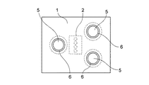
図8及び図9は、特許文献1に記載の技術を応用した光コネクタの一例を示す平面図及び側面図であって、これらの図に示すように、本例の光コネクタは、ベースプレート1と、当該ベースプレート1に備えられた第1のマイクロレンズ群2と、図示しない光変調器(E/O)及び光復調器(O/E)等が実装された基板3と、当該基板3に備えられた第2のマイクロレンズ群4と、基板3上に接着等により取り付けられて、第2のマイクロレンズ群4の周囲に配置された複数本(図8の例では、3本)の位置決めピン5とを有している。なお、第1乃至第2のマイクロレンズ群2,4を構成する各レンズは、コリメータレンズである。ベースプレート1には、位置決めピン5の設定部と対応する位置に、位置決めピン5を嵌合可能なピン係合孔6が開設されており、当該ピン係合孔6内に位置決めピン5を嵌合することによって、第1のマイクロレンズ群2を構成する各マイクロレンズの光軸と、第2のマイクロレンズ群4を構成する各マイクロレンズの光軸とを合致させている。これにより、第1のマイクロレンズ群2を構成する各マイクロレンズと、第2のマイクロレンズ群4を構成する各マイクロレンズとの間の光結合損失を防止できて、良好な光伝送効率を実現することができる。
8 and 9 are a plan view and a side view showing an example of an optical connector to which the technology described in
ところで、上記構成の光コネクタは、ベースプレート1についてはステンレスやアルミニウム等の金属板をもって形成され、基板3についてはガラスエポキシ等の複合材や樹脂材料をもって形成されるのが普通である。このため、製造時に、所定の温度条件(例えば、常温)で、第1のマイクロレンズ群2を構成する各マイクロレンズの光軸と、第2のマイクロレンズ群4を構成する各マイクロレンズの光軸とを厳密に合致したとしても、環境温度が変化して、ベースプレート1と基板3とがそれぞれの線膨張係数に応じた量だけ面方向に伸縮した場合には、各マイクロレンズの光軸がずれ、光結合損失を生じるという問題がある。
By the way, in the optical connector having the above-described configuration, the
本発明は、かかる技術的課題を解決するためになされたものであり、その目的は、環境温度の変化に応じて、線膨張係数が異なる材料からなるベースプレートと基板とが伸縮した場合にも、これらの各部材に備えられた各マイクロレンズの光軸ずれ、ひいてはこれに起因する光結合損失の発生を防止することができる光コネクタを提供することにある。 The present invention has been made in order to solve such a technical problem, and its purpose is that even when a base plate and a substrate made of materials having different linear expansion coefficients expand and contract according to changes in environmental temperature, An object of the present invention is to provide an optical connector capable of preventing the optical axis shift of each microlens provided in each of these members, and hence the occurrence of optical coupling loss resulting therefrom.
本発明は、前記課題を解決するため、ベースプレートと、当該ベースプレートに備えられた第1のマイクロレンズと、前記ベースプレートとは線膨張係数が異なる材料にて形成された基板と、当該基板に備えられた第2のマイクロレンズと、当該第2のマイクロレンズの周囲に配置されて、前記基板上に取り付けられた複数本の位置決めピンと、前記ベースプレートに開設され、前記位置決めピンと協働して前記第1のマイクロレンズの光軸と前記第2のマイクロレンズの光軸とを合致させるピン係合孔とを備えた光コネクタにおいて、前記位置決めピンの先端部は、前記位置決めピンの先端側に至るに従って直径が小さくなるテーパ面又は半球面に形成され、前記ピン係合孔は、前記位置決めピンの先端部と係合したときに、前記テーパ面に沿う方向又は前記半球面の接線に沿う方向の分力を生じる形状に形成され、前記ベースプレートは、前記ピン係合孔内に前記位置決めピンの先端部を挿入し、かつ前記ベースプレートの上面側から前記基板側に弾性力を付与することによって、前記位置決めピン及び前記基板と一体化されており、環境温度が変化したとき、前記テーパ面に沿う方向又は前記半球面の接線に沿う方向の分力により、前記ベースプレートと前記基板との線膨張係数の差に応じた変位量だけ、前記弾性力に抗して、前記基板から離隔する方向に変位するという構成にした。 In order to solve the above problems, the present invention includes a base plate, a first microlens provided in the base plate, a substrate formed of a material having a linear expansion coefficient different from that of the base plate, and the substrate. A second microlens, a plurality of positioning pins disposed around the second microlens and mounted on the substrate, and provided in the base plate, and in cooperation with the positioning pins, the first microlens. In the optical connector provided with a pin engaging hole for matching the optical axis of the microlens and the optical axis of the second microlens, the distal end portion of the positioning pin has a diameter as it reaches the distal end side of the positioning pin. Is formed into a tapered surface or a hemispherical surface, and the pin engaging hole is engaged with the tip end portion of the positioning pin when the tapered surface is formed. The base plate is formed in a shape that generates a component force in a direction along or along a tangent line of the hemispherical surface, and the base plate inserts the tip end portion of the positioning pin into the pin engaging hole, and the upper side of the base plate By applying elastic force to the substrate side, it is integrated with the positioning pin and the substrate, and when the environmental temperature changes, the component force in the direction along the taper surface or the tangential line of the hemisphere The base plate and the substrate are displaced in the direction away from the substrate against the elastic force by the amount of displacement corresponding to the difference in linear expansion coefficient.
かかる構成によると、環境温度の変化に起因して、ベースプレートと基板とが、その線膨張係数に応じた伸縮量だけ伸縮した場合、位置決めピンとピン係合孔との間に作用するテーパ面に沿う方向又は半球面の接線に沿う方向の分力が増加するので、ベースプレートが、これに付与される弾性力に抗して基板から離隔する方向に変位する。したがって、ベースプレートと基板との間に伸縮差が生じた場合にも、ベースプレートと基板とが面方向に関して相対的に変位せず、ベースプレートに備えられた第1のマイクロレンズと基板に備えられた第2のマイクロレンズとの光軸ずれを防止することができる。 According to such a configuration, when the base plate and the substrate expand and contract by an amount of expansion and contraction corresponding to the linear expansion coefficient due to a change in environmental temperature, the taper surface that acts between the positioning pin and the pin engagement hole is aligned. Since the component force in the direction or the direction along the tangent line of the hemisphere increases, the base plate is displaced in a direction away from the substrate against the elastic force applied thereto. Therefore, even when an expansion / contraction difference occurs between the base plate and the substrate, the base plate and the substrate are not relatively displaced with respect to the surface direction, and the first microlens provided on the base plate and the first micro lens provided on the substrate are provided. It is possible to prevent the optical axis from being shifted with respect to the second microlens.
また、本発明は、前記ベースプレートに弾性力を付与するための手段として、前記位置決めピンの頂部に螺合されるボルトと、当該ボルトの頭部と前記ベースプレートの上面との間に配置されるスプリングワッシャとを用いるという構成にした。 Further, according to the present invention, as means for applying an elastic force to the base plate, a bolt screwed to the top of the positioning pin, and a spring disposed between the head of the bolt and the upper surface of the base plate It was configured to use a washer.
かかる構成によると、ボルトの締付トルクを加減することにより、ベースプレートに付与される弾性力を種々加減することができるので、ベースプレートに付与される弾性力が異なる各種の光コネクタを容易に製造することができる。 According to such a configuration, by adjusting the bolt tightening torque, various elastic forces applied to the base plate can be adjusted. Therefore, various optical connectors having different elastic forces applied to the base plate can be easily manufactured. be able to.
また、本発明は、前記ベースプレートに弾性力を付与するための手段として、両端部を前記ベースプレートと前記基板とにそれぞれ係合する、金属板からなるクリップ部材を用いるという構成にした。 In the present invention, as a means for applying an elastic force to the base plate, a clip member made of a metal plate that engages both ends with the base plate and the substrate is used.
かかる構成によると、所要のばね定数を有するクリップ部材をベースプレートと基板とに係合するだけで光コネクタの組立を行うことができるので、光コネクタの製造を容易なものにすることができる。 According to such a configuration, since the optical connector can be assembled only by engaging the clip member having a required spring constant with the base plate and the substrate, the optical connector can be easily manufactured.
また、本発明は、前記ベースプレートに弾性力を付与するための手段として、前記ベースプレートの上面に接する上部材と、前記基板の下面に接する下部材とからなり、前記ベースプレートと前記基板との間に弾性力を付与した状態で一体に結合される筐体を用いるという構成にした。 Further, the present invention includes an upper member that is in contact with the upper surface of the base plate and a lower member that is in contact with the lower surface of the substrate, as means for applying an elastic force to the base plate, and between the base plate and the substrate. A case is used in which a casing that is integrally coupled with an elastic force applied is used.
かかる構成によると、ベースプレートに弾性力を付与するための特別な部品を用意する必要がないので、部品点数の減少及び組み立て工程の簡略化を図ることができて、光コネクタの低コスト化を図ることができる。 According to such a configuration, it is not necessary to prepare a special part for applying an elastic force to the base plate, so that the number of parts can be reduced and the assembly process can be simplified, and the cost of the optical connector can be reduced. be able to.
本発明の光コネクタは、環境温度が変化したとき、ベースプレートが基板から離隔する方向に変位するという構成にしたので、ベースプレートに備えられた第1のマイクロレンズと基板に備えられた第2のマイクロレンズとの光軸ずれを防止でき、光結合損失の発生による光伝送効率の劣化を防止することができる。 Since the optical connector of the present invention is configured such that when the environmental temperature changes, the base plate is displaced in a direction away from the substrate, the first microlens provided on the base plate and the second microlens provided on the substrate are arranged. The optical axis deviation from the lens can be prevented, and the deterioration of the optical transmission efficiency due to the occurrence of optical coupling loss can be prevented.
まず、本発明に係る光コネクタの第1実施形態を、図1乃至図4に基づいて説明する。本例の光コネクタは、位置決めピンの先端部の形状をテーパ面としたこと、並びにベースプレートに弾性力を付与するための手段として、ボルト7及びスプリングワッシャ8を用いたことを特徴とする。
First, a first embodiment of an optical connector according to the present invention will be described with reference to FIGS. The optical connector of this example is characterized in that the shape of the tip portion of the positioning pin is a tapered surface, and the
図1乃至図3に示すように、本例の光コネクタも、基本的な構成に関しては、図6及び図7に示した従来例に係る光コネクタと同じであり、ベースプレート1と、当該ベースプレート1に備えられた第1のマイクロレンズ群2と、図示しない光変調器(E/O)及び光復調器(O/E)等が実装された基板3と、当該基板3に備えられた第2のマイクロレンズ群4と、基板3上に接着等により取り付けられて、第2のマイクロレンズ群4の周囲に配置された複数本(図6の例では、3本)の位置決めピン5とを有している。また、ベースプレート1には、位置決めピン5の設定部と対応する位置に、位置決めピン5を嵌合可能なピン係合孔6が開設されており、当該ピン係合孔6内に位置決めピン5を嵌合することによって、第1のマイクロレンズ群2を構成する各マイクロレンズ2a〜2dの光軸と、第2のマイクロレンズ群4を構成する各マイクロレンズ4a〜4dの光軸とを合致させている。ベースプレート1は、ステンレスやアルミニウム等の金属板をもって形成され、基板3は、ガラスエポキシ等の複合材や樹脂材料をもって形成されている。また、各マイクロレンズ2a〜2d,4a〜4dとしては、コリメータレンズが用いられる。
As shown in FIGS. 1 to 3, the optical connector of this example is the same as the optical connector according to the conventional example shown in FIGS. 6 and 7 with respect to the basic configuration, and includes a
本実施形態においては、図2及び図3に示すように、位置決めピン5の先端部が先端側に至るに従って直径が一様に減少するテーパ面になっており、ピン係合孔6も、これと同一傾斜のテーパ面になっている。位置決めピン5には、その頂面に貫通するねじ孔5aが開設されており、このねじ孔5aには、ベースプレート1のピン係合孔6を貫通したボルト7が螺合される。ボルト7とベースプレート1との間には、スプリングワッシャ8が介設されており、ボルト7は、スプリングワッシャ8がその弾性限を超えて締め付けられない範囲の所要のトルクでベースプレート1に締め付けられる。したがって、ベースプレート1は、上向き(図2に示す矢印Yの向き)の力を受けたとき、スプリングワッシャ8の弾性力に抗して、基板3から離隔する方向に変位することができる。
In this embodiment, as shown in FIGS. 2 and 3, the tip of the
上述のように、本例の光コネクタは、ベースプレート1がステンレスやアルミニウム等の金属板をもって形成され、基板3がガラスエポキシ等の複合材や樹脂材料をもって形成されているので、環境温度が変化した場合、ベースプレート1と基板3とは、それぞれ固有の線膨張係数に応じた異なる伸縮量だけ伸縮し、面方向の長さ寸法に相違を生じる。本例の光コネクタは、位置決めピン5の先端部がテーパ面になっており、ピン係合孔6も、これと同一傾斜のテーパ面になっているので、ベースプレート1と位置決めピン5との間に、ベースプレート1と基板3の伸縮量の差に応じた水平方向の力Fhが作用した場合、図4に示すように、ベースプレート1と位置決めピン5の接触部に、テーパ面に沿った上向きの分力Faと、テーパ面に垂直な方向の分力Fbとを生じ、その合力である垂直上向きのベースプレート上昇力Fvが発生する。これにより、ベースプレート1は、基板3から離隔する方向に変位し、ベースプレート1と基板3とが面方向に相対的に変位することがない。
As described above, in the optical connector of this example, the
ベースプレート1の変位について、図3を基にさらに詳細に説明すると、環境温度が高くなった場合には、ガラスエポキシ等で形成された基板3の伸び量が金属等で形成されたベースプレート1の伸び量よりも大きくなり、図3に矢印イで示すように、基板3がベースプレート1に対して右方向に相対的に変位するので、位置決めピン5のテーパ面5bがピン係合孔6の外側部分6aに強く接触する。これにより、図3に矢印ハで示すように、ベースプレート1が、位置決めピン5のテーパ面6aに沿って押し上げられる。一方、環境温度が低くなった場合には、ガラスエポキシ等で形成された基板3の収縮量が金属等で形成されたベースプレート1の収縮量よりも大きくなり、図3に矢印ロで示すように、基板3がベースプレート1に対して左方向に相対的に変位するので、位置決めピン5のテーパ面6aがピン係合孔6の内側部分5cに強く接触する。これにより、この場合にも、図3に矢印ハで示すように、ベースプレート1が、位置決めピン5のテーパ面6aに沿って押し上げられる。
The displacement of the
したがって、第1のマイクロレンズ群2を構成する各マイクロレンズ2a〜2dの光軸と、第2のマイクロレンズ群4を構成する各マイクロレンズ4a〜4dの光軸とのずれをなくすことができて、これに起因する光結合損失を解消することができる。また、マイクロレンズ2a〜2d,4a〜4dとしては、コリメータレンズが用いられているので、ベースプレート1が基板3から離隔する方向に変位した場合にも、これに起因する光結合損失を解消することができる。また、上述したように、環境温度が高くなった場合にも、低くなった場合にも、ベースプレートに設けられた第1のマイクロレンズ群2と基板に設けられた第2のマイクロレンズ群4とは、離隔する方向に変位するので、これら第1のマイクロレンズ群2と第2のマイクロレンズ群4との距離を最小に設定することができ、光コネクタの薄型化を図ることができる。
Accordingly, it is possible to eliminate the deviation between the optical axes of the
次に、本発明に係る光コネクタの第2実施形態を、図5に基づいて説明する。本例の光コネクタは、位置決めピン5の先端部の形状を球面状としたことを特徴とする。その他については、第1実施形態に係る光コネクタと同じであるので、対応する部分に同一の符号を付して説明を省略する。
Next, a second embodiment of the optical connector according to the present invention will be described with reference to FIG. The optical connector of this example is characterized in that the shape of the tip of the
本例の光コネクタは、第1実施形態に係る光コネクタと同様の効果を奏するほか、位置決めピン5の先端部の形状を球面状としたので、位置決めピン5とピン係合孔6との間に作用する摩擦力を低減することができて、位置決めピン5に対するベースプレート1の上下動を円滑なものにすることができる。
The optical connector of this example has the same effect as the optical connector according to the first embodiment, and the shape of the tip of the
次に、本発明に係る光コネクタの第3実施形態を、図6に基づいて説明する。本例の光コネクタは、ベースプレート1と基板3とを、ボルト7ではなく、クリップ9を用いて一体に結合したことを特徴とする。クリップ9は、ステンレスなどの弾性に優れた金属板を用いて、断面形状が略コの字形に形成される。その他については、第1実施形態に係る光コネクタと同じであるので、対応する部分に同一の符号を付して説明を省略する。
Next, a third embodiment of the optical connector according to the present invention will be described with reference to FIG. The optical connector of this example is characterized in that the
本例の光コネクタは、第1実施形態に係る光コネクタと同様の効果を奏するほか、クリップ9を用いてベースプレート1と基板3とを結合したので、ベースプレート1と基板3との組立を容易化できて、光コネクタの製造を容易なものにすることができる。
The optical connector of this example has the same effect as the optical connector according to the first embodiment, and the
次に、本発明に係る光コネクタの第4実施形態を、図7に基づいて説明する。本例の光コネクタは、ベースプレート1の上面に接する上部材11と、基板3の下面に接する下部材12とからなる筐体13を用いて、ベースプレート1と基板3とを一体に結合したことを特徴とする。上部材11及び下部材12は、ステンレスなどの弾性に優れた金属板を用いて形成され、ベースプレート1と基板3との間に弾性力を付与した状態で一体に結合される。その他については、第1実施形態に係る光コネクタと同じであるので、対応する部分に同一の符号を付して説明を省略する。
Next, a fourth embodiment of the optical connector according to the present invention will be described with reference to FIG. The optical connector of this example is obtained by integrally bonding the
本例の光コネクタは、第1実施形態に係る光コネクタと同様の効果を奏するほか、筐体13を用いてベースプレート1と基板3とを一体に結合するので、ベースプレート1に弾性力を付与するための特別な部品を用意する必要がなく、部品点数の減少及び組み立て工程の簡略化を図ることができて、光コネクタの低コスト化を図ることができる。
The optical connector of this example has the same effect as that of the optical connector according to the first embodiment. In addition, since the
なお、前記各実施形態においては、位置決めピン5の本数を3本としたが、2本又は4本以上の数とすることもできる。
In each of the above embodiments, the number of
以下に、具体的な実施例を挙げて、本発明の効果を明らかにする。 Hereinafter, specific examples will be given to clarify the effects of the present invention.
ベースプレート1を線膨張係数が1.7×10−5/℃のステンレスをもって形成し、基板3を線膨張係数が6×10−5/℃のガラスエポキシをもって形成した。また、位置決めピン5の設定ピッチ及びピン係合孔6の開設ピッチを10mmとした。この場合において、環境温度が25℃から85℃まで60℃上昇すると、ベースプレート1については、ピン係合孔6の開設ピッチの増加が10.2μm程度であるのに対して、基板3については、位置決めピン5の設定ピッチの増加が36μm程度になり、ベースプレート1と基板3との間に、25.8μm程度のピッチずれが発生する。なお、実際にマイクロレンズ群2,4の光軸ずれが発生するのは、位置決めピン5の設定ピッチの中間位置であるので、該部におけるピッチずれは、その半分の12.9μm程度になるものと想定される。これは、マイクロレンズ群2,4に14.9%の光結合損失が生じるピッチずれに相当する。一方、本願の構成において、位置決めピン5及びピン係合孔6に形成されるテーパ面のテーパを45°とした場合、ベースプレート1は、基板3から12.9μm程度上方に離隔する方向に変位する。これによって、ベースプレート1に設けられた第1のマイクロレンズ群2と基板3に設けられた第2のマイクロレンズ群4との光軸ずれが防止される。
The
1 ベースプレート
2 第1のマイクロレンズ群
2a〜2d 第1のマイクロレンズ群を構成する各マイクロレンズ
3 基板
4 第2のマイクロレンズ群
4a〜4d 第2のマイクロレンズ群を構成する各マイクロレンズ
5 位置決めピン
5a ねじ孔
6 ピン係合孔
7 ボルト
8 スプリングワッシャ
9 クリップ
11 上部材
12 下部材
13 筐体
DESCRIPTION OF
Claims (4)
前記位置決めピンの先端部は、前記位置決めピンの先端側に至るに従って直径が小さくなるテーパ面又は半球面に形成され、前記ピン係合孔は、前記位置決めピンの先端部と係合したときに、前記テーパ面に沿う方向又は前記半球面の接線に沿う方向の分力を生じる形状に形成され、
前記ベースプレートは、前記ピン係合孔内に前記位置決めピンの先端部を挿入し、かつ前記ベースプレートの上面側から前記基板側に弾性力を付与することによって、前記位置決めピン及び前記基板と一体化されており、環境温度が変化したとき、前記テーパ面に沿う方向又は前記半球面の接線に沿う方向の分力により、前記ベースプレートと前記基板との線膨張係数の差に応じた変位量だけ、前記弾性力に抗して、前記基板から離隔する方向に変位することを特徴とする光コネクタ。 A base plate, a first microlens provided in the base plate, a substrate formed of a material having a linear expansion coefficient different from that of the base plate, a second microlens provided in the substrate, and the second And a plurality of positioning pins mounted on the substrate and provided on the base plate, and in cooperation with the positioning pins, the optical axis of the first microlens and the second microlens. In an optical connector having a pin engagement hole that matches the optical axis of the microlens,
The distal end portion of the positioning pin is formed in a tapered surface or a hemispheric surface whose diameter decreases as it reaches the distal end side of the positioning pin, and the pin engagement hole is engaged with the distal end portion of the positioning pin. It is formed in a shape that produces a component force in a direction along the tapered surface or in a direction along the tangent line of the hemispherical surface,
The base plate is integrated with the positioning pin and the substrate by inserting the tip end portion of the positioning pin into the pin engaging hole and applying an elastic force from the upper surface side of the base plate to the substrate side. When the environmental temperature changes, the component force in the direction along the taper surface or in the direction along the tangent line of the hemispherical surface, the displacement amount corresponding to the difference in linear expansion coefficient between the base plate and the substrate, An optical connector which is displaced in a direction away from the substrate against an elastic force.
Priority Applications (1)
| Application Number | Priority Date | Filing Date | Title |
|---|---|---|---|
| JP2009132381A JP5117445B2 (en) | 2009-06-01 | 2009-06-01 | Optical connector |
Applications Claiming Priority (1)
| Application Number | Priority Date | Filing Date | Title |
|---|---|---|---|
| JP2009132381A JP5117445B2 (en) | 2009-06-01 | 2009-06-01 | Optical connector |
Publications (2)
| Publication Number | Publication Date |
|---|---|
| JP2010277045A JP2010277045A (en) | 2010-12-09 |
| JP5117445B2 true JP5117445B2 (en) | 2013-01-16 |
Family
ID=43424029
Family Applications (1)
| Application Number | Title | Priority Date | Filing Date |
|---|---|---|---|
| JP2009132381A Expired - Fee Related JP5117445B2 (en) | 2009-06-01 | 2009-06-01 | Optical connector |
Country Status (1)
| Country | Link |
|---|---|
| JP (1) | JP5117445B2 (en) |
Family Cites Families (3)
| Publication number | Priority date | Publication date | Assignee | Title |
|---|---|---|---|---|
| JP2006258835A (en) * | 2005-03-15 | 2006-09-28 | Sony Corp | Optical waveguide module, photoelectric conversion device, and optical waveguide member |
| JP4229112B2 (en) * | 2005-11-15 | 2009-02-25 | ヤマハ株式会社 | Manufacturing method of micro lens array |
| JP4690963B2 (en) * | 2006-08-09 | 2011-06-01 | 株式会社日立製作所 | Manufacturing method of multi-channel optical module |
-
2009
- 2009-06-01 JP JP2009132381A patent/JP5117445B2/en not_active Expired - Fee Related
Also Published As
| Publication number | Publication date |
|---|---|
| JP2010277045A (en) | 2010-12-09 |
Similar Documents
| Publication | Publication Date | Title |
|---|---|---|
| US9658423B2 (en) | Springless athermal lens design with flexured spacer | |
| US7884688B2 (en) | Waveguide connector and assembly using deformable convex conductive portions | |
| US7625132B2 (en) | Packaging for a fiber-coupled optical device | |
| US8256972B2 (en) | Fiber optic connector and fiber optic assembly having same | |
| US7869146B2 (en) | Lens module | |
| KR20110034257A (en) | All-in-one camera module | |
| CN102985707A (en) | Lock nut and a fastening unit comprising the same | |
| US20190258019A1 (en) | Optical apparatus and camera module | |
| CN103328809A (en) | Fuel injection valve with improved high pressure interface | |
| JP5117445B2 (en) | Optical connector | |
| JP4214406B2 (en) | Semiconductor device having optical signal input / output mechanism | |
| JP2006330121A (en) | The camera module | |
| TWM616391U (en) | Easy to lock and easy to unlock connector | |
| US20110096515A1 (en) | Electronic device and fabrication method thereof | |
| KR101264552B1 (en) | Cable lead-out structure | |
| CN112384836A (en) | Optical connecting component | |
| JP6852574B2 (en) | Optical module and manufacturing method of optical module | |
| JP2014182202A (en) | Electronic equipment, and optical connector | |
| JP2006330120A (en) | The camera module | |
| KR101514892B1 (en) | Electrical connector and Electrical connector assembly including the same | |
| US9482832B2 (en) | Optical coupling component with metal positioning rods and optical-electrical converting module having same | |
| JP5896462B2 (en) | Optical system unit, camera module | |
| CN211577529U (en) | Optical imaging system | |
| KR101597130B1 (en) | A spring connection | |
| CN116931189A (en) | Optical fiber connector with adjustable sleeve |
Legal Events
| Date | Code | Title | Description |
|---|---|---|---|
| A621 | Written request for application examination |
Free format text: JAPANESE INTERMEDIATE CODE: A621 Effective date: 20110915 |
|
| A977 | Report on retrieval |
Free format text: JAPANESE INTERMEDIATE CODE: A971007 Effective date: 20120910 |
|
| TRDD | Decision of grant or rejection written | ||
| A01 | Written decision to grant a patent or to grant a registration (utility model) |
Free format text: JAPANESE INTERMEDIATE CODE: A01 Effective date: 20121002 |
|
| A01 | Written decision to grant a patent or to grant a registration (utility model) |
Free format text: JAPANESE INTERMEDIATE CODE: A01 |
|
| A61 | First payment of annual fees (during grant procedure) |
Free format text: JAPANESE INTERMEDIATE CODE: A61 Effective date: 20121017 |
|
| R150 | Certificate of patent or registration of utility model |
Free format text: JAPANESE INTERMEDIATE CODE: R150 Ref document number: 5117445 Country of ref document: JP Free format text: JAPANESE INTERMEDIATE CODE: R150 |
|
| FPAY | Renewal fee payment (event date is renewal date of database) |
Free format text: PAYMENT UNTIL: 20151026 Year of fee payment: 3 |
|
| S533 | Written request for registration of change of name |
Free format text: JAPANESE INTERMEDIATE CODE: R313533 |
|
| R350 | Written notification of registration of transfer |
Free format text: JAPANESE INTERMEDIATE CODE: R350 |
|
| LAPS | Cancellation because of no payment of annual fees |