JP5120004B2 - 基板の表面処理方法および半導体パッケージの製造方法 - Google Patents
基板の表面処理方法および半導体パッケージの製造方法 Download PDFInfo
- Publication number
- JP5120004B2 JP5120004B2 JP2008077308A JP2008077308A JP5120004B2 JP 5120004 B2 JP5120004 B2 JP 5120004B2 JP 2008077308 A JP2008077308 A JP 2008077308A JP 2008077308 A JP2008077308 A JP 2008077308A JP 5120004 B2 JP5120004 B2 JP 5120004B2
- Authority
- JP
- Japan
- Prior art keywords
- substrate
- region
- semiconductor package
- surface treatment
- film
- Prior art date
- Legal status (The legal status is an assumption and is not a legal conclusion. Google has not performed a legal analysis and makes no representation as to the accuracy of the status listed.)
- Expired - Fee Related
Links
Images

Classifications
-
- H—ELECTRICITY
- H10—SEMICONDUCTOR DEVICES; ELECTRIC SOLID-STATE DEVICES NOT OTHERWISE PROVIDED FOR
- H10W—GENERIC PACKAGES, INTERCONNECTIONS, CONNECTORS OR OTHER CONSTRUCTIONAL DETAILS OF DEVICES COVERED BY CLASS H10
- H10W72/00—Interconnections or connectors in packages
- H10W72/851—Dispositions of multiple connectors or interconnections
- H10W72/874—On different surfaces
- H10W72/884—Die-attach connectors and bond wires
-
- H—ELECTRICITY
- H10—SEMICONDUCTOR DEVICES; ELECTRIC SOLID-STATE DEVICES NOT OTHERWISE PROVIDED FOR
- H10W—GENERIC PACKAGES, INTERCONNECTIONS, CONNECTORS OR OTHER CONSTRUCTIONAL DETAILS OF DEVICES COVERED BY CLASS H10
- H10W90/00—Package configurations
- H10W90/701—Package configurations characterised by the relative positions of pads or connectors relative to package parts
- H10W90/731—Package configurations characterised by the relative positions of pads or connectors relative to package parts of die-attach connectors
- H10W90/734—Package configurations characterised by the relative positions of pads or connectors relative to package parts of die-attach connectors between a chip and a stacked insulating package substrate, interposer or RDL
-
- H—ELECTRICITY
- H10—SEMICONDUCTOR DEVICES; ELECTRIC SOLID-STATE DEVICES NOT OTHERWISE PROVIDED FOR
- H10W—GENERIC PACKAGES, INTERCONNECTIONS, CONNECTORS OR OTHER CONSTRUCTIONAL DETAILS OF DEVICES COVERED BY CLASS H10
- H10W90/00—Package configurations
- H10W90/701—Package configurations characterised by the relative positions of pads or connectors relative to package parts
- H10W90/751—Package configurations characterised by the relative positions of pads or connectors relative to package parts of bond wires
- H10W90/754—Package configurations characterised by the relative positions of pads or connectors relative to package parts of bond wires between a chip and a stacked insulating package substrate, interposer or RDL
Landscapes
- Drying Of Semiconductors (AREA)
- Encapsulation Of And Coatings For Semiconductor Or Solid State Devices (AREA)
Description
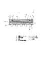
の割合が高くなっているが、表面処理装置20を用いた表面処理によれば、第1の領域に対してアッシングによる表面処理を施すと同時に第2の領域には成膜用ターゲットの組成物質を付着させる成膜処理を施すことで、両領域の面積比に関係なく基板3の表面の略全面において樹脂密着性を向上させることが可能である。
2 半導体装置
3 基板
6 ワイヤ接続用電極
10 レジスト膜
12 封止用の樹脂
20 表面処理装置
21 密閉空間
22 真空チャンバ
23 基板保持ステージ
24 成膜用ターゲット
25 成膜用ターゲット保持部
26 減圧装置
27 放電用ガス供給装置
28 高周波電源部
31 多面取基板
32 有機膜
Claims (10)
- 樹脂が露出する第1の領域と金メッキ膜が露出する第2の領域を表面に有する基板の表面処理方法であって、
真空チャンバ内に基板の表面と成膜用ターゲットとを対向させて配置し、真空チャンバ内に放電用ガスを供給してプラズマを発生させることで前記第1の領域のアッシングと前記成膜用ターゲットのスパッタリングを行い、前記第1の領域の活性化処理と前記第2の領域に前記成膜用ターゲットの組成物質を付着させる成膜処理とを並行して行うことを特徴とする基板の表面処理方法。 - 前記成膜用ターゲットが組成物質にSiO2を含むことを特徴とする請求項1記載の基板の表面処理方法。
- 前記放電用ガスに少なくともアルゴンと酸素を含むことを特徴とする請求項1または2記載の基板の表面処理方法。
- 基板の表面に露出する樹脂がソルダレジストであることを特徴とする請求項1乃至3の何れかに記載の基板の表面処理方法。
- 前記第1の領域に、基板に実装された半導体装置の表面を覆う有機膜を含むことを特徴とする請求項1乃至4の何れかに記載の基板の表面処理方法。
- 樹脂が露出する第1の領域と金メッキ膜が露出する第2の領域を表面に有する基板の表面に半導体装置を実装する工程と、真空チャンバ内に基板の表面と成膜用ターゲットとを間隔をおいて対向配置し、真空チャンバ内に放電用ガスを供給してプラズマを発生させることで前記第1の領域のアッシングと前記成膜用ターゲットのスパッタリングを行い、前記第1の領域の活性化処理と前記第2の領域に前記成膜用ターゲットの組成物質を付着させる成膜処理とを並行して行う表面処理工程と、表面処理された基板の表面を樹脂で封止する工程を含むことを特徴とする半導体パッケージの製造方法。
- 前記成膜用ターゲットが組成物質にSiO2を含むことを特徴とする請求項6に記載の半導体パッケージの製造方法。
- 前記放電用ガスに少なくともアルゴンと酸素を含むことを特徴とする請求項6または7に記載の半導体パッケージの製造方法。
- 前記表面に露出する樹脂がソルダレジストであることを特徴とする請求項6乃至8の何れかに記載の半導体パッケージの製造方法。
- 前記第1の領域に、基板に搭載された半導体装置の表面を覆う有機膜を含むことを特徴とする請求項6乃至9の何れかに記載の半導体パッケージの製造方法。
Priority Applications (1)
| Application Number | Priority Date | Filing Date | Title |
|---|---|---|---|
| JP2008077308A JP5120004B2 (ja) | 2008-03-25 | 2008-03-25 | 基板の表面処理方法および半導体パッケージの製造方法 |
Applications Claiming Priority (1)
| Application Number | Priority Date | Filing Date | Title |
|---|---|---|---|
| JP2008077308A JP5120004B2 (ja) | 2008-03-25 | 2008-03-25 | 基板の表面処理方法および半導体パッケージの製造方法 |
Publications (2)
| Publication Number | Publication Date |
|---|---|
| JP2009231680A JP2009231680A (ja) | 2009-10-08 |
| JP5120004B2 true JP5120004B2 (ja) | 2013-01-16 |
Family
ID=41246727
Family Applications (1)
| Application Number | Title | Priority Date | Filing Date |
|---|---|---|---|
| JP2008077308A Expired - Fee Related JP5120004B2 (ja) | 2008-03-25 | 2008-03-25 | 基板の表面処理方法および半導体パッケージの製造方法 |
Country Status (1)
| Country | Link |
|---|---|
| JP (1) | JP5120004B2 (ja) |
Families Citing this family (1)
| Publication number | Priority date | Publication date | Assignee | Title |
|---|---|---|---|---|
| EP2415891A4 (en) | 2009-04-03 | 2014-11-19 | Kobe Steel Ltd | COLD-ROLLED STEEL PLATE AND METHOD FOR THE PRODUCTION THEREOF |
Family Cites Families (4)
| Publication number | Priority date | Publication date | Assignee | Title |
|---|---|---|---|---|
| JP2681167B2 (ja) * | 1988-10-12 | 1997-11-26 | 株式会社半導体エネルギー研究所 | 電子装置作製方法 |
| JPH1131759A (ja) * | 1997-07-14 | 1999-02-02 | Sony Corp | 吸湿保護膜を有する実装回路基板及び実装回路基板の吸湿保護膜形成方法 |
| JP2001259411A (ja) * | 2000-03-16 | 2001-09-25 | Matsushita Electric Ind Co Ltd | プラズマ処理方法 |
| JP3671879B2 (ja) * | 2001-07-17 | 2005-07-13 | 松下電器産業株式会社 | 電子部品製造方法および電子部品 |
-
2008
- 2008-03-25 JP JP2008077308A patent/JP5120004B2/ja not_active Expired - Fee Related
Also Published As
| Publication number | Publication date |
|---|---|
| JP2009231680A (ja) | 2009-10-08 |
Similar Documents
| Publication | Publication Date | Title |
|---|---|---|
| US8421168B2 (en) | Microelectromechanical systems microphone packaging systems | |
| TWI502654B (zh) | 半導體裝置及包括研磨步驟之半導體裝置的製造方法 | |
| US5909633A (en) | Method of manufacturing an electronic component | |
| US10229870B2 (en) | Packaged semiconductor device with tensile stress and method of making a packaged semiconductor device with tensile stress | |
| JP2004319892A (ja) | 半導体装置の製造方法 | |
| KR20030023571A (ko) | 반도체 칩 표면의 플라즈마 처리에 의한 접착 성능 개선방법 | |
| CN107039292B (zh) | 元件芯片的制造方法、电子部件安装构造体的制造方法 | |
| US7019404B2 (en) | Multilayered circuit substrate, semiconductor device and method of producing same | |
| TW200913194A (en) | Semiconductor package and manufacturing method thereof | |
| CN103855122B (zh) | 包括压缩应力的封装垂直功率器件及其制造方法 | |
| CN108011608A (zh) | 一种应用于声表面波滤波器的晶圆级封装结构及封装工艺 | |
| WO2007099759A1 (ja) | 部品接合方法、部品積層方法および部品接合構造体 | |
| JP2011100793A5 (ja) | 半導体パッケージ及びその製造方法 | |
| JP5120004B2 (ja) | 基板の表面処理方法および半導体パッケージの製造方法 | |
| US20080290514A1 (en) | Semiconductor device package and method of fabricating the same | |
| JP2020004857A (ja) | 半導体装置の製造方法 | |
| CN102446837B (zh) | 包括半导体芯片的器件的制造 | |
| JP3671879B2 (ja) | 電子部品製造方法および電子部品 | |
| JP3427702B2 (ja) | 電子部品のプラズマ処理装置 | |
| JP2006202974A (ja) | 電子装置及びその製造方法 | |
| JPH10340977A (ja) | 電子部品およびその製造方法 | |
| US8093101B2 (en) | Electronic device and method of fabricating the same | |
| KR100824542B1 (ko) | 배선용 봉지층을 이용한 웨이퍼 레벨 패키지 제조방법 | |
| JP2006196619A (ja) | 電子装置及びその製造方法 | |
| JP4462221B2 (ja) | 半導体部品の製造方法 |
Legal Events
| Date | Code | Title | Description |
|---|---|---|---|
| A621 | Written request for application examination |
Free format text: JAPANESE INTERMEDIATE CODE: A621 Effective date: 20100127 |
|
| RD01 | Notification of change of attorney |
Free format text: JAPANESE INTERMEDIATE CODE: A7421 Effective date: 20100215 |
|
| A977 | Report on retrieval |
Free format text: JAPANESE INTERMEDIATE CODE: A971007 Effective date: 20100419 |
|
| A131 | Notification of reasons for refusal |
Free format text: JAPANESE INTERMEDIATE CODE: A131 Effective date: 20120508 |
|
| A521 | Request for written amendment filed |
Free format text: JAPANESE INTERMEDIATE CODE: A523 Effective date: 20120622 |
|
| TRDD | Decision of grant or rejection written | ||
| A01 | Written decision to grant a patent or to grant a registration (utility model) |
Free format text: JAPANESE INTERMEDIATE CODE: A01 Effective date: 20120925 |
|
| A01 | Written decision to grant a patent or to grant a registration (utility model) |
Free format text: JAPANESE INTERMEDIATE CODE: A01 |
|
| A61 | First payment of annual fees (during grant procedure) |
Free format text: JAPANESE INTERMEDIATE CODE: A61 Effective date: 20121008 |
|
| FPAY | Renewal fee payment (event date is renewal date of database) |
Free format text: PAYMENT UNTIL: 20151102 Year of fee payment: 3 |
|
| FPAY | Renewal fee payment (event date is renewal date of database) |
Free format text: PAYMENT UNTIL: 20151102 Year of fee payment: 3 |
|
| LAPS | Cancellation because of no payment of annual fees |