JP5146019B2 - 高周波モジュールとこれを用いた電子機器 - Google Patents
高周波モジュールとこれを用いた電子機器 Download PDFInfo
- Publication number
- JP5146019B2 JP5146019B2 JP2008057452A JP2008057452A JP5146019B2 JP 5146019 B2 JP5146019 B2 JP 5146019B2 JP 2008057452 A JP2008057452 A JP 2008057452A JP 2008057452 A JP2008057452 A JP 2008057452A JP 5146019 B2 JP5146019 B2 JP 5146019B2
- Authority
- JP
- Japan
- Prior art keywords
- shield
- terminal
- substrate
- ground
- conductor
- Prior art date
- Legal status (The legal status is an assumption and is not a legal conclusion. Google has not performed a legal analysis and makes no representation as to the accuracy of the status listed.)
- Expired - Fee Related
Links
Images


Classifications
-
- H—ELECTRICITY
- H10—SEMICONDUCTOR DEVICES; ELECTRIC SOLID-STATE DEVICES NOT OTHERWISE PROVIDED FOR
- H10W—GENERIC PACKAGES, INTERCONNECTIONS, CONNECTORS OR OTHER CONSTRUCTIONAL DETAILS OF DEVICES COVERED BY CLASS H10
- H10W42/00—Arrangements for protection of devices
- H10W42/20—Arrangements for protection of devices protecting against electromagnetic or particle radiation, e.g. light, X-rays, gamma-rays or electrons
-
- H—ELECTRICITY
- H10—SEMICONDUCTOR DEVICES; ELECTRIC SOLID-STATE DEVICES NOT OTHERWISE PROVIDED FOR
- H10W—GENERIC PACKAGES, INTERCONNECTIONS, CONNECTORS OR OTHER CONSTRUCTIONAL DETAILS OF DEVICES COVERED BY CLASS H10
- H10W90/00—Package configurations
- H10W90/701—Package configurations characterised by the relative positions of pads or connectors relative to package parts
- H10W90/721—Package configurations characterised by the relative positions of pads or connectors relative to package parts of bump connectors
- H10W90/724—Package configurations characterised by the relative positions of pads or connectors relative to package parts of bump connectors between a chip and a stacked insulating package substrate, interposer or RDL
Landscapes
- Production Of Multi-Layered Print Wiring Board (AREA)
- Printing Elements For Providing Electric Connections Between Printed Circuits (AREA)
- Shielding Devices Or Components To Electric Or Magnetic Fields (AREA)
- Structure Of Printed Boards (AREA)
Description
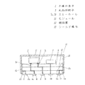
以下、本実施の形態について図面を用いて説明する。図1は本実施の形態におけるモジュールの断面図である。図1において本実施の形態におけるモジュール1では、半導体素子2や水晶振動子3などの複数個の電子部品が基板4の表面に実装され、基板4上に高周波回路が形成されている。基板4の表側にはシールドカバー5(シールド導体の一例として用いた)が装着され、シールドカバー5がこれらの電子部品を覆う構造を有している。なお、本実施の形態において基板4には、4層の多層基板を用いている。
以下、本実施の形態について図面を用いて説明する。図4は、本実施の形態におけるモジュールの断面図である。図4において、図1と同じものには、同じ番号を用いて、その説明は簡略化している。
2 半導体素子
3 水晶振動子
4 基板
5 シールドカバー
5a 脚
6 グランドパターン
7a スルーホール
7b スルーホール
8 グランド端子
9a スルーホール
9b スルーホール
10a 信号端子
10b 信号端子
11 シールド端子
12 接続導体
12a スルーホール
12b 中継パターン
12c 接続部
21 電子機器
22 マザー基板
31 モジュール
32 樹脂層
33 シールド導体
Claims (2)
- 基板と、この基板の表面に電子部品が搭載されて形成された高周波回路と、この高周波回路のグランドと接続されたグランドパターンと、このグランドパターンに対し第1のスルーホールを介して接続されるとともに前記基板の裏面に設けられたグランド端子と、前記基板の裏面に設けられるとともに、前記高周波回路と接続された信号端子と、前記高周波回路を覆う金属製のシールド導体と、前記シールド導体に接続されるとともに、前記基板の裏面に設けられたシールド端子と、前記基板の内層に設けられ、前記シールド導体と前記シールド端子との間を接続する接続導体とを備え、前記グランドパターンおよび前記グランド端子とは共に、前記シールド導体ならびに前記シールド端子と分離されて設けられ、前記シールド端子は、グランド端子と前記信号端子とを囲うように配置されるとともに、複数個のシールド端子が断続して配置されることによって形成され、前記シールド端子同士の間隔は、前記高周波回路における最も高い周波数の波長の4分の1以下の長さとした高周波モジュールにおいて、シールド導体は、基板の側面全周に設けられるとともに、前記接続導体は、前記シールド端子と接続された複数個の第2のスルーホールと、これらの第2のスルーホールに接続された中継パターンと、この中継パターンに接続され、かつ前記シールド導体と接続される接続部を含み、これらの第2のスルーホール同士の間隔は、高周波回路における最も高い周波数の波長の4分の1以下の距離とした高周波モジュール。
- マザー基板と、このマザー基板上に装着された請求項1に記載の高周波モジュールとを備え、前記高周波モジュールの裏面には、隣接したシールド端子の間に設けられた前記シールド端子不形成部を設けるとともに、前記マザー基板には、配線パターンと、グランド端子と信号端子およびシールド端子のそれぞれと対応する位置に設けられた接続ランドが形成され、前記配線パターンは前記マザー基板において前記不形成部に対応する位置を通して配線された電子機器。
Priority Applications (1)
| Application Number | Priority Date | Filing Date | Title |
|---|---|---|---|
| JP2008057452A JP5146019B2 (ja) | 2008-03-07 | 2008-03-07 | 高周波モジュールとこれを用いた電子機器 |
Applications Claiming Priority (1)
| Application Number | Priority Date | Filing Date | Title |
|---|---|---|---|
| JP2008057452A JP5146019B2 (ja) | 2008-03-07 | 2008-03-07 | 高周波モジュールとこれを用いた電子機器 |
Publications (2)
| Publication Number | Publication Date |
|---|---|
| JP2009218258A JP2009218258A (ja) | 2009-09-24 |
| JP5146019B2 true JP5146019B2 (ja) | 2013-02-20 |
Family
ID=41189865
Family Applications (1)
| Application Number | Title | Priority Date | Filing Date |
|---|---|---|---|
| JP2008057452A Expired - Fee Related JP5146019B2 (ja) | 2008-03-07 | 2008-03-07 | 高周波モジュールとこれを用いた電子機器 |
Country Status (1)
| Country | Link |
|---|---|
| JP (1) | JP5146019B2 (ja) |
Families Citing this family (6)
| Publication number | Priority date | Publication date | Assignee | Title |
|---|---|---|---|---|
| JP6508920B2 (ja) | 2014-11-13 | 2019-05-08 | 太陽誘電株式会社 | 弾性波デバイスおよび送受信デバイス |
| WO2018139046A1 (ja) * | 2017-01-27 | 2018-08-02 | 株式会社村田製作所 | インターポーザ基板、回路モジュール、インターポーザ基板の製造方法 |
| CN111033722B (zh) | 2017-09-04 | 2023-12-12 | 株式会社村田制作所 | 高频模块及其制造方法 |
| JP7571649B2 (ja) * | 2021-03-31 | 2024-10-23 | 株式会社デンソー | 電子装置 |
| KR20220164305A (ko) | 2021-06-04 | 2022-12-13 | 삼성전자주식회사 | 전자 장치에서의 쉴드 구조 및 그 동작 방법 |
| JP7632924B1 (ja) | 2024-02-16 | 2025-02-19 | Necプラットフォームズ株式会社 | シールド部品、電子機器、及び、シールド部品の製造方法 |
-
2008
- 2008-03-07 JP JP2008057452A patent/JP5146019B2/ja not_active Expired - Fee Related
Also Published As
| Publication number | Publication date |
|---|---|
| JP2009218258A (ja) | 2009-09-24 |
Similar Documents
| Publication | Publication Date | Title |
|---|---|---|
| JP6753514B2 (ja) | 高周波モジュール | |
| US8102669B2 (en) | Chip package structure with shielding cover | |
| JP5750528B1 (ja) | 部品内蔵回路基板 | |
| US20080003846A1 (en) | Circuit board unit | |
| JP2009218258A (ja) | 高周波モジュール | |
| JP6973667B2 (ja) | 回路基板及び電子機器 | |
| CN110506454B (zh) | 基板间连接构造 | |
| WO2018164159A1 (ja) | モジュール | |
| JP2015176966A (ja) | 電子機器 | |
| EP1594353A1 (en) | High frequency multilayer printed wiring board | |
| JP4692152B2 (ja) | 回路モジュール及びその製造方法 | |
| JP5577716B2 (ja) | 回路モジュール及び回路モジュールの製造方法 | |
| WO2014061202A1 (ja) | コネクタ | |
| JPWO2008010445A1 (ja) | 多層プリント回路基板 | |
| US20220310317A1 (en) | Electronic component module | |
| JPWO2006093155A1 (ja) | 基板間接続コネクタ及び基板間接続コネクタを用いた回路基板装置 | |
| US7414321B2 (en) | Wiring configuration for semiconductor component | |
| JP2014053445A (ja) | 回路基板および複合モジュール | |
| CN101404277A (zh) | 多芯片模块 | |
| JP2006211620A (ja) | フィルタ及びデュプレクサ | |
| JP2008112832A (ja) | 高周波ユニット、及び高周波ユニットの製造方法 | |
| JP5642559B2 (ja) | 電子部品モジュール | |
| US20070089901A1 (en) | Circuit board providing coplanarity of solders and high soldering reliability for semiconductor component | |
| JP2008034672A (ja) | チップ部品の実装方法および電子モジュール | |
| JP2011108719A (ja) | 高周波装置 |
Legal Events
| Date | Code | Title | Description |
|---|---|---|---|
| A621 | Written request for application examination |
Free format text: JAPANESE INTERMEDIATE CODE: A621 Effective date: 20100308 |
|
| RD01 | Notification of change of attorney |
Free format text: JAPANESE INTERMEDIATE CODE: A7421 Effective date: 20100413 |
|
| A977 | Report on retrieval |
Free format text: JAPANESE INTERMEDIATE CODE: A971007 Effective date: 20111031 |
|
| A131 | Notification of reasons for refusal |
Free format text: JAPANESE INTERMEDIATE CODE: A131 Effective date: 20111115 |
|
| A521 | Request for written amendment filed |
Free format text: JAPANESE INTERMEDIATE CODE: A523 Effective date: 20111213 |
|
| A131 | Notification of reasons for refusal |
Free format text: JAPANESE INTERMEDIATE CODE: A131 Effective date: 20120626 |
|
| A521 | Request for written amendment filed |
Free format text: JAPANESE INTERMEDIATE CODE: A523 Effective date: 20120801 |
|
| TRDD | Decision of grant or rejection written | ||
| A01 | Written decision to grant a patent or to grant a registration (utility model) |
Free format text: JAPANESE INTERMEDIATE CODE: A01 Effective date: 20121030 |
|
| A61 | First payment of annual fees (during grant procedure) |
Free format text: JAPANESE INTERMEDIATE CODE: A61 Effective date: 20121112 |
|
| FPAY | Renewal fee payment (event date is renewal date of database) |
Free format text: PAYMENT UNTIL: 20151207 Year of fee payment: 3 |
|
| LAPS | Cancellation because of no payment of annual fees |