JP5152352B2 - 液晶表示用基板及び液晶表示装置 - Google Patents
液晶表示用基板及び液晶表示装置 Download PDFInfo
- Publication number
- JP5152352B2 JP5152352B2 JP2011019833A JP2011019833A JP5152352B2 JP 5152352 B2 JP5152352 B2 JP 5152352B2 JP 2011019833 A JP2011019833 A JP 2011019833A JP 2011019833 A JP2011019833 A JP 2011019833A JP 5152352 B2 JP5152352 B2 JP 5152352B2
- Authority
- JP
- Japan
- Prior art keywords
- liquid crystal
- crystal display
- pattern
- pixel
- display device
- Prior art date
- Legal status (The legal status is an assumption and is not a legal conclusion. Google has not performed a legal analysis and makes no representation as to the accuracy of the status listed.)
- Expired - Fee Related
Links
Images





Classifications
-
- G—PHYSICS
- G02—OPTICS
- G02F—OPTICAL DEVICES OR ARRANGEMENTS FOR THE CONTROL OF LIGHT BY MODIFICATION OF THE OPTICAL PROPERTIES OF THE MEDIA OF THE ELEMENTS INVOLVED THEREIN; NON-LINEAR OPTICS; FREQUENCY-CHANGING OF LIGHT; OPTICAL LOGIC ELEMENTS; OPTICAL ANALOGUE/DIGITAL CONVERTERS
- G02F1/00—Devices or arrangements for the control of the intensity, colour, phase, polarisation or direction of light arriving from an independent light source, e.g. switching, gating or modulating; Non-linear optics
- G02F1/01—Devices or arrangements for the control of the intensity, colour, phase, polarisation or direction of light arriving from an independent light source, e.g. switching, gating or modulating; Non-linear optics for the control of the intensity, phase, polarisation or colour
- G02F1/13—Devices or arrangements for the control of the intensity, colour, phase, polarisation or direction of light arriving from an independent light source, e.g. switching, gating or modulating; Non-linear optics for the control of the intensity, phase, polarisation or colour based on liquid crystals, e.g. single liquid crystal display cells
- G02F1/1323—Arrangements for providing a switchable viewing angle
-
- G—PHYSICS
- G02—OPTICS
- G02F—OPTICAL DEVICES OR ARRANGEMENTS FOR THE CONTROL OF LIGHT BY MODIFICATION OF THE OPTICAL PROPERTIES OF THE MEDIA OF THE ELEMENTS INVOLVED THEREIN; NON-LINEAR OPTICS; FREQUENCY-CHANGING OF LIGHT; OPTICAL LOGIC ELEMENTS; OPTICAL ANALOGUE/DIGITAL CONVERTERS
- G02F1/00—Devices or arrangements for the control of the intensity, colour, phase, polarisation or direction of light arriving from an independent light source, e.g. switching, gating or modulating; Non-linear optics
- G02F1/01—Devices or arrangements for the control of the intensity, colour, phase, polarisation or direction of light arriving from an independent light source, e.g. switching, gating or modulating; Non-linear optics for the control of the intensity, phase, polarisation or colour
- G02F1/13—Devices or arrangements for the control of the intensity, colour, phase, polarisation or direction of light arriving from an independent light source, e.g. switching, gating or modulating; Non-linear optics for the control of the intensity, phase, polarisation or colour based on liquid crystals, e.g. single liquid crystal display cells
- G02F1/133—Constructional arrangements; Operation of liquid crystal cells; Circuit arrangements
- G02F1/1333—Constructional arrangements; Manufacturing methods
- G02F1/1343—Electrodes
-
- G—PHYSICS
- G02—OPTICS
- G02F—OPTICAL DEVICES OR ARRANGEMENTS FOR THE CONTROL OF LIGHT BY MODIFICATION OF THE OPTICAL PROPERTIES OF THE MEDIA OF THE ELEMENTS INVOLVED THEREIN; NON-LINEAR OPTICS; FREQUENCY-CHANGING OF LIGHT; OPTICAL LOGIC ELEMENTS; OPTICAL ANALOGUE/DIGITAL CONVERTERS
- G02F1/00—Devices or arrangements for the control of the intensity, colour, phase, polarisation or direction of light arriving from an independent light source, e.g. switching, gating or modulating; Non-linear optics
- G02F1/01—Devices or arrangements for the control of the intensity, colour, phase, polarisation or direction of light arriving from an independent light source, e.g. switching, gating or modulating; Non-linear optics for the control of the intensity, phase, polarisation or colour
- G02F1/13—Devices or arrangements for the control of the intensity, colour, phase, polarisation or direction of light arriving from an independent light source, e.g. switching, gating or modulating; Non-linear optics for the control of the intensity, phase, polarisation or colour based on liquid crystals, e.g. single liquid crystal display cells
- G02F1/133—Constructional arrangements; Operation of liquid crystal cells; Circuit arrangements
- G02F1/1333—Constructional arrangements; Manufacturing methods
-
- G—PHYSICS
- G02—OPTICS
- G02F—OPTICAL DEVICES OR ARRANGEMENTS FOR THE CONTROL OF LIGHT BY MODIFICATION OF THE OPTICAL PROPERTIES OF THE MEDIA OF THE ELEMENTS INVOLVED THEREIN; NON-LINEAR OPTICS; FREQUENCY-CHANGING OF LIGHT; OPTICAL LOGIC ELEMENTS; OPTICAL ANALOGUE/DIGITAL CONVERTERS
- G02F1/00—Devices or arrangements for the control of the intensity, colour, phase, polarisation or direction of light arriving from an independent light source, e.g. switching, gating or modulating; Non-linear optics
- G02F1/01—Devices or arrangements for the control of the intensity, colour, phase, polarisation or direction of light arriving from an independent light source, e.g. switching, gating or modulating; Non-linear optics for the control of the intensity, phase, polarisation or colour
- G02F1/13—Devices or arrangements for the control of the intensity, colour, phase, polarisation or direction of light arriving from an independent light source, e.g. switching, gating or modulating; Non-linear optics for the control of the intensity, phase, polarisation or colour based on liquid crystals, e.g. single liquid crystal display cells
- G02F1/133—Constructional arrangements; Operation of liquid crystal cells; Circuit arrangements
- G02F1/1333—Constructional arrangements; Manufacturing methods
- G02F1/1335—Structural association of cells with optical devices, e.g. polarisers or reflectors
-
- G—PHYSICS
- G02—OPTICS
- G02F—OPTICAL DEVICES OR ARRANGEMENTS FOR THE CONTROL OF LIGHT BY MODIFICATION OF THE OPTICAL PROPERTIES OF THE MEDIA OF THE ELEMENTS INVOLVED THEREIN; NON-LINEAR OPTICS; FREQUENCY-CHANGING OF LIGHT; OPTICAL LOGIC ELEMENTS; OPTICAL ANALOGUE/DIGITAL CONVERTERS
- G02F1/00—Devices or arrangements for the control of the intensity, colour, phase, polarisation or direction of light arriving from an independent light source, e.g. switching, gating or modulating; Non-linear optics
- G02F1/01—Devices or arrangements for the control of the intensity, colour, phase, polarisation or direction of light arriving from an independent light source, e.g. switching, gating or modulating; Non-linear optics for the control of the intensity, phase, polarisation or colour
- G02F1/13—Devices or arrangements for the control of the intensity, colour, phase, polarisation or direction of light arriving from an independent light source, e.g. switching, gating or modulating; Non-linear optics for the control of the intensity, phase, polarisation or colour based on liquid crystals, e.g. single liquid crystal display cells
- G02F1/133—Constructional arrangements; Operation of liquid crystal cells; Circuit arrangements
- G02F1/1333—Constructional arrangements; Manufacturing methods
- G02F1/1335—Structural association of cells with optical devices, e.g. polarisers or reflectors
- G02F1/133509—Filters, e.g. light shielding masks
- G02F1/133512—Light shielding layers, e.g. black matrix
-
- G—PHYSICS
- G02—OPTICS
- G02F—OPTICAL DEVICES OR ARRANGEMENTS FOR THE CONTROL OF LIGHT BY MODIFICATION OF THE OPTICAL PROPERTIES OF THE MEDIA OF THE ELEMENTS INVOLVED THEREIN; NON-LINEAR OPTICS; FREQUENCY-CHANGING OF LIGHT; OPTICAL LOGIC ELEMENTS; OPTICAL ANALOGUE/DIGITAL CONVERTERS
- G02F1/00—Devices or arrangements for the control of the intensity, colour, phase, polarisation or direction of light arriving from an independent light source, e.g. switching, gating or modulating; Non-linear optics
- G02F1/01—Devices or arrangements for the control of the intensity, colour, phase, polarisation or direction of light arriving from an independent light source, e.g. switching, gating or modulating; Non-linear optics for the control of the intensity, phase, polarisation or colour
- G02F1/13—Devices or arrangements for the control of the intensity, colour, phase, polarisation or direction of light arriving from an independent light source, e.g. switching, gating or modulating; Non-linear optics for the control of the intensity, phase, polarisation or colour based on liquid crystals, e.g. single liquid crystal display cells
- G02F1/133—Constructional arrangements; Operation of liquid crystal cells; Circuit arrangements
- G02F1/1333—Constructional arrangements; Manufacturing methods
- G02F1/1337—Surface-induced orientation of the liquid crystal molecules, e.g. by alignment layers
- G02F1/133707—Structures for producing distorted electric fields, e.g. bumps, protrusions, recesses, slits in pixel electrodes
-
- G—PHYSICS
- G02—OPTICS
- G02F—OPTICAL DEVICES OR ARRANGEMENTS FOR THE CONTROL OF LIGHT BY MODIFICATION OF THE OPTICAL PROPERTIES OF THE MEDIA OF THE ELEMENTS INVOLVED THEREIN; NON-LINEAR OPTICS; FREQUENCY-CHANGING OF LIGHT; OPTICAL LOGIC ELEMENTS; OPTICAL ANALOGUE/DIGITAL CONVERTERS
- G02F1/00—Devices or arrangements for the control of the intensity, colour, phase, polarisation or direction of light arriving from an independent light source, e.g. switching, gating or modulating; Non-linear optics
- G02F1/01—Devices or arrangements for the control of the intensity, colour, phase, polarisation or direction of light arriving from an independent light source, e.g. switching, gating or modulating; Non-linear optics for the control of the intensity, phase, polarisation or colour
- G02F1/13—Devices or arrangements for the control of the intensity, colour, phase, polarisation or direction of light arriving from an independent light source, e.g. switching, gating or modulating; Non-linear optics for the control of the intensity, phase, polarisation or colour based on liquid crystals, e.g. single liquid crystal display cells
- G02F1/133—Constructional arrangements; Operation of liquid crystal cells; Circuit arrangements
- G02F1/136—Liquid crystal cells structurally associated with a semi-conducting layer or substrate, e.g. cells forming part of an integrated circuit
- G02F1/1362—Active matrix addressed cells
- G02F1/1368—Active matrix addressed cells in which the switching element is a three-electrode device
-
- G—PHYSICS
- G02—OPTICS
- G02F—OPTICAL DEVICES OR ARRANGEMENTS FOR THE CONTROL OF LIGHT BY MODIFICATION OF THE OPTICAL PROPERTIES OF THE MEDIA OF THE ELEMENTS INVOLVED THEREIN; NON-LINEAR OPTICS; FREQUENCY-CHANGING OF LIGHT; OPTICAL LOGIC ELEMENTS; OPTICAL ANALOGUE/DIGITAL CONVERTERS
- G02F1/00—Devices or arrangements for the control of the intensity, colour, phase, polarisation or direction of light arriving from an independent light source, e.g. switching, gating or modulating; Non-linear optics
- G02F1/01—Devices or arrangements for the control of the intensity, colour, phase, polarisation or direction of light arriving from an independent light source, e.g. switching, gating or modulating; Non-linear optics for the control of the intensity, phase, polarisation or colour
- G02F1/13—Devices or arrangements for the control of the intensity, colour, phase, polarisation or direction of light arriving from an independent light source, e.g. switching, gating or modulating; Non-linear optics for the control of the intensity, phase, polarisation or colour based on liquid crystals, e.g. single liquid crystal display cells
- G02F1/133—Constructional arrangements; Operation of liquid crystal cells; Circuit arrangements
- G02F1/1333—Constructional arrangements; Manufacturing methods
- G02F1/1335—Structural association of cells with optical devices, e.g. polarisers or reflectors
- G02F1/133509—Filters, e.g. light shielding masks
- G02F1/133514—Colour filters
-
- G—PHYSICS
- G02—OPTICS
- G02F—OPTICAL DEVICES OR ARRANGEMENTS FOR THE CONTROL OF LIGHT BY MODIFICATION OF THE OPTICAL PROPERTIES OF THE MEDIA OF THE ELEMENTS INVOLVED THEREIN; NON-LINEAR OPTICS; FREQUENCY-CHANGING OF LIGHT; OPTICAL LOGIC ELEMENTS; OPTICAL ANALOGUE/DIGITAL CONVERTERS
- G02F1/00—Devices or arrangements for the control of the intensity, colour, phase, polarisation or direction of light arriving from an independent light source, e.g. switching, gating or modulating; Non-linear optics
- G02F1/01—Devices or arrangements for the control of the intensity, colour, phase, polarisation or direction of light arriving from an independent light source, e.g. switching, gating or modulating; Non-linear optics for the control of the intensity, phase, polarisation or colour
- G02F1/13—Devices or arrangements for the control of the intensity, colour, phase, polarisation or direction of light arriving from an independent light source, e.g. switching, gating or modulating; Non-linear optics for the control of the intensity, phase, polarisation or colour based on liquid crystals, e.g. single liquid crystal display cells
- G02F1/133—Constructional arrangements; Operation of liquid crystal cells; Circuit arrangements
- G02F1/1333—Constructional arrangements; Manufacturing methods
- G02F1/1343—Electrodes
- G02F1/134309—Electrodes characterised by their geometrical arrangement
- G02F1/134336—Matrix
-
- G—PHYSICS
- G02—OPTICS
- G02F—OPTICAL DEVICES OR ARRANGEMENTS FOR THE CONTROL OF LIGHT BY MODIFICATION OF THE OPTICAL PROPERTIES OF THE MEDIA OF THE ELEMENTS INVOLVED THEREIN; NON-LINEAR OPTICS; FREQUENCY-CHANGING OF LIGHT; OPTICAL LOGIC ELEMENTS; OPTICAL ANALOGUE/DIGITAL CONVERTERS
- G02F1/00—Devices or arrangements for the control of the intensity, colour, phase, polarisation or direction of light arriving from an independent light source, e.g. switching, gating or modulating; Non-linear optics
- G02F1/01—Devices or arrangements for the control of the intensity, colour, phase, polarisation or direction of light arriving from an independent light source, e.g. switching, gating or modulating; Non-linear optics for the control of the intensity, phase, polarisation or colour
- G02F1/13—Devices or arrangements for the control of the intensity, colour, phase, polarisation or direction of light arriving from an independent light source, e.g. switching, gating or modulating; Non-linear optics for the control of the intensity, phase, polarisation or colour based on liquid crystals, e.g. single liquid crystal display cells
- G02F1/133—Constructional arrangements; Operation of liquid crystal cells; Circuit arrangements
- G02F1/1333—Constructional arrangements; Manufacturing methods
- G02F1/1343—Electrodes
- G02F1/134309—Electrodes characterised by their geometrical arrangement
- G02F1/134381—Hybrid switching mode, i.e. for applying an electric field with components parallel and orthogonal to the substrates
-
- G—PHYSICS
- G02—OPTICS
- G02F—OPTICAL DEVICES OR ARRANGEMENTS FOR THE CONTROL OF LIGHT BY MODIFICATION OF THE OPTICAL PROPERTIES OF THE MEDIA OF THE ELEMENTS INVOLVED THEREIN; NON-LINEAR OPTICS; FREQUENCY-CHANGING OF LIGHT; OPTICAL LOGIC ELEMENTS; OPTICAL ANALOGUE/DIGITAL CONVERTERS
- G02F1/00—Devices or arrangements for the control of the intensity, colour, phase, polarisation or direction of light arriving from an independent light source, e.g. switching, gating or modulating; Non-linear optics
- G02F1/01—Devices or arrangements for the control of the intensity, colour, phase, polarisation or direction of light arriving from an independent light source, e.g. switching, gating or modulating; Non-linear optics for the control of the intensity, phase, polarisation or colour
- G02F1/13—Devices or arrangements for the control of the intensity, colour, phase, polarisation or direction of light arriving from an independent light source, e.g. switching, gating or modulating; Non-linear optics for the control of the intensity, phase, polarisation or colour based on liquid crystals, e.g. single liquid crystal display cells
- G02F1/137—Devices or arrangements for the control of the intensity, colour, phase, polarisation or direction of light arriving from an independent light source, e.g. switching, gating or modulating; Non-linear optics for the control of the intensity, phase, polarisation or colour based on liquid crystals, e.g. single liquid crystal display cells characterised by the electro-optical or magneto-optical effect, e.g. field-induced phase transition, orientation effect, guest-host interaction or dynamic scattering
- G02F1/139—Devices or arrangements for the control of the intensity, colour, phase, polarisation or direction of light arriving from an independent light source, e.g. switching, gating or modulating; Non-linear optics for the control of the intensity, phase, polarisation or colour based on liquid crystals, e.g. single liquid crystal display cells characterised by the electro-optical or magneto-optical effect, e.g. field-induced phase transition, orientation effect, guest-host interaction or dynamic scattering based on orientation effects in which the liquid crystal remains transparent
-
- G—PHYSICS
- G02—OPTICS
- G02F—OPTICAL DEVICES OR ARRANGEMENTS FOR THE CONTROL OF LIGHT BY MODIFICATION OF THE OPTICAL PROPERTIES OF THE MEDIA OF THE ELEMENTS INVOLVED THEREIN; NON-LINEAR OPTICS; FREQUENCY-CHANGING OF LIGHT; OPTICAL LOGIC ELEMENTS; OPTICAL ANALOGUE/DIGITAL CONVERTERS
- G02F2203/00—Function characteristic
- G02F2203/64—Normally black display, i.e. the off state being black
Landscapes
- Physics & Mathematics (AREA)
- Nonlinear Science (AREA)
- Chemical & Material Sciences (AREA)
- Crystallography & Structural Chemistry (AREA)
- General Physics & Mathematics (AREA)
- Optics & Photonics (AREA)
- Mathematical Physics (AREA)
- Spectroscopy & Molecular Physics (AREA)
- Liquid Crystal (AREA)
- Engineering & Computer Science (AREA)
- Microelectronics & Electronic Packaging (AREA)
Description
本実施形態においては、初期垂直配向の液晶又は初期水平配向の液晶を備えるノーマリーブラックの液晶表示装置について説明する。本実施形態においては、サブピクセル単位の構成について説明するが、本実施形態と同様の構成を画素単位に適用してもよい。
本実施形態においては、上記第1の実施形態に係る液晶表示用基板2に用いられる透明樹脂及び有機顔料などの各種の材料の例について説明する。
遮光層あるいは着色層の形成に用いられる感光性着色組成物は、顔料分散体に加え、さらに、多官能モノマー、感光性樹脂又は非感光性樹脂、重合開始剤、溶剤等を含有する。感光性樹脂又は非感光性樹脂などのような本実施形態で用いられる透明性の高い有機樹脂を総称して透明樹脂と呼ぶ。
本実施形態に用いられる遮光パターン6、透明パターン5、着色サブピクセルの形成には、フォトリソグラフィによるパターン形成可能な感光性樹脂組成物を用いることが好ましい。これらの透明樹脂は、アルカリ可溶性を与えられた樹脂であることが望ましい。アルカリ可溶性樹脂としては、カルボキシル基又は水酸基を含む樹脂であればよい。例えば、アルカリ可溶性樹脂としては、エポキシアクリレート系樹脂、ノボラック系樹脂、ポリビニルフェノール系樹脂、アクリル系樹脂、カルボキシル基含有エポキシ樹脂、カルボキシル基含有ウレタン樹脂等が用いられる。これらの中でも、エポキシアクリレート系樹脂、ノボラック系樹脂、アクリル系樹脂が好ましく、特に、エポキシアクリレート系樹脂又はノボラック系樹脂が好ましい。
本実施形態に係る透明樹脂の代表として、以下のアクリル系樹脂が例示できる。
赤色顔料としては、例えば、C.I.Pigment Red 7、9、14、41、48:1、48:2、48:3、48:4、81:1、81:2、81:3、97、122、123、146、149、168、177、178、179、180、184、185、187、192、200、202、208、210、215、216、217、220、223、224、226、227、228、240、242、246、254、255、264、272、279等を用いることができる。
遮光層あるいはマトリクスパターンに含まれる遮光性の色材は、可視光波長領域に吸収特性を有することにより遮光機能を実現する。本実施形態において遮光性の色材には、例えば、有機顔料、無機顔料、染料等が用いられる。無機顔料としては、例えば、カーボンブラック、酸化チタン等が用いられる。染料としては、例えば、アゾ系染料、アントラキノン系染料、フタロシアニン系染料、キノンイミン系染料、キノリン系染料、ニトロ系染料、カルボニル系染料、メチン系染料等が用いられる。有機顔料については、先で説明した有機顔料を用いるとしてもよい。なお、遮光性成分は、1種を用いてもよく、2種以上を任意の組み合わせ及び比率で併用してもよい。また、これら色材の表面における樹脂被覆による高体積抵抗化を行ってもよい。逆に、樹脂の母材に対して色材の含有比率を上げて若干の導電性を付与することによる低体積抵抗化を行ってもよい。このような遮光性材料の体積抵抗値は、およそ1×10⁸〜1×10¹⁵Ω・cmの範囲であるため、透明導電膜の抵抗値に影響するレベルではない。同様に、遮光層の比誘電率も色材の選択又は含有比率でおよそ3〜20の範囲で調整できる。遮光パターン6、透明パターン7、着色層(カラーフィルタ10〜12)、保護層14の比誘電率は、液晶表示装置1の設計条件と液晶の駆動条件とのうちの少なくとも一方に基づいて調整できる。
顔料分散剤として高分子分散剤を用いることは、経時の分散安定性に優れるため、好ましい。高分子分散剤としては、例えば、ウレタン系分散剤、ポリエチレンイミン系分散剤、ポリオキシエチレンアルキルエーテル系分散剤、ポリオキシエチレングリコールジエステル系分散剤、ソルビタン脂肪族エステル系分散剤、脂肪族変性ポリエステル系分散剤等を用いることができる。特に、顔料を多く含む遮光性感光性樹脂組成物に対しては、窒素原子を含有するグラフト共重合体を含む分散剤が用いられることが、現像性の観点から好ましい。分散剤は、1種を用いてもよく、2種以上を任意の組み合わせ及び比率で併用してもよい。
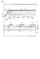
本実施形態においては、図16に示す液晶表示用基板2Aの製造方法の一例について説明する。図16は、液晶表示用基板2Aの基板9を上とし、保護層14を下として図示している。
(遮光パターン6形成用分散液)
カーボン顔料#47 20質量部、高分子分散剤 8.3質量部、銅フタロシアニン誘導体 1.0質量部、及びプロピレングリコールモノメチルエーテルアセテート71質量部を、ビーズミル分散機にて攪拌し、カーボンブラック分散液が生成される。
遮光層の材料として遮光パターン6形成用レジストが、以下の材料を使用して生成される。
透明樹脂(固形分56.1質量%)
光重合性モノマー
開始剤
溶剤:プロピレングリコールモノメチルエーテルアセテート、エチル-3-エトキシプロピオネート
レベリング剤
遮光パターン6形成用レジスト(固形分中の顔料濃度:約20%)は、上記の材料を、以下の組成比で混合攪拌して生成される。
透明樹脂 1.4質量部
光重合性モノマー 0.4質量部
第1の光重合開始剤 0.67質量部
第2の光重合開始剤 0.17質量部
プロピレングリコールモノメチルエーテルアセテート 14質量部
エチル-3-エトキシプロピオネート 5.0質量部
レベリング剤 1.5質量部
(遮光パターン形成条件)
無アルカリガラスである透明基板9上に、上記遮光パターン6形成用レジストをスピンコートし、乾燥させ、膜厚1.5μmの塗膜が生成される。この塗膜が100℃で3分間、乾燥された後、露光用のフォトマスクを用い、光源として超高圧水銀灯ランプを用いて200mJ/cm2の照射が実行される。
(樹脂Aの合成)
セパラブルフラスコ中で、プロピレングリコールモノメチルエーテルアセテート686質量部、グリシジルメタクリレート 332質量部、アゾビスイソブチロニトリル 6.6質量部を加え、窒素雰囲気下において80℃で6時間加熱し、樹脂溶液が生成される。
以下の組成にて、ネガ型の感光性樹脂液AAが生成される。
光重合性モノマー
ジペンタエリスリトールヘキサアクリレート 100質量部
光重合開始剤 100質量部
溶剤(プロピレングリコールモノメチルエーテルアセテート) 380質量部
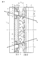
感光性樹脂液AA及び透明パターン5(開口部)のあるフォトマスクを使用し、公知のフォトリスグラフィ法にて、図1に示す8μm幅の遮光パターン6の間に18μm幅の透明パターン5が、透明基板9上に形成され、34μm幅の線状パターン7及びマトリクスパターンが生成される。透明パターン5の高さ(膜厚)は、例えば3.2μmとする。
スパッタリング装置を用いて、線状パターン7及びマトリクスパターンの全面を覆うように、第3電極13として、ITO(インジウム・スズの金属酸化物薄膜)などのような、可視域で透明な透明導電膜が0.14μmの膜厚で形成される。
(樹脂Bの合成)
反応容器にシクロヘキサノン 800部を入れ、容器に窒素ガスを注入しながら加熱して、下記のモノマーおよび熱重合開始剤の混合物を滴下して重合反応が行われる。
メタクリル酸 60質量部
メチルメタクリレート 65質量部
ブチルメタクリレート 65質量部
熱重合開始剤 10質量部
連鎖移動剤 3質量部
滴下後十分に加熱した後、熱重合開始剤 2.0質量部をシクロヘキサノン 50部で溶解させた材料を添加し、さらに反応を続けてアクリル樹脂の溶液が生成される。
下記組成の混合物を均一に拡販混合した後、直径1mmのガラスビーズを用いて、サンドミルで5時間分散した後、1μmのフィルタで濾過して樹脂塗布液BBが生成される。
多官能重合性モノマー 20質量部
光開始剤 16質量部
シクロヘキサノン 250質量部
樹脂塗布液BBを用い、第3電極13の全面を覆うように保護層14を塗布、乾燥させる。次に、透明パターン5の形状と同じ遮光パターンを持つフォトマスクを用い、露光・現像が行われ、透明パターン5上部の保護層14が除去される。その後、全面再露光と熱処理により保護層14が硬膜され、液晶表示用基板2Aが形成される。硬膜後の保護層14の膜圧は、多角形サブピクセル中央部で2.0μmである。線状パターン7頂部の多角形サブピクセルの第3電極13の表面の高さから、サブピクセル中央部の保護層14表面までの高さの差は、約1.2μmとする。
本実施形態においては、上記図2に示す液晶表示用基板2の製造方法の一例について説明する。図2は、製造された液晶表示用基板2の基板9を上とし、保護層14を下として図示している。
(着色層形成用分散液)
着色層に分散する有機顔料として、例えば以下の顔料が用いられる。
緑色顔料:C.I.Pigment Green 58、C.I.Pigment Yellow 150
青色顔料:C.I.Pigment Blue 15、C.I.Pigment Violet 23
上記の顔料を用いて、赤色、緑色、及び青色の各色分散液が生成される。
赤色顔料:C.I.Pigment Red 254 18質量部
赤色顔料:C.I.Pigment Red 177 2質量部
アクリルワニス(固形分20質量%) 108質量部
上記の組成の混合物を均一に攪拌した後、ガラスビーズを用いて、サンドミルで5時間分散し、5μmフィルタで濾過し、赤色分散液が生成される。
緑色顔料:C.I.Pigment Green 58 16質量部
緑色顔料:C.I.Pigment Yellow 150 8質量部
アクリルワニス(固形分20質量%) 102質量部
上記の組成の混合物に対して、赤色分散液と同様の生成方法を用いて、緑色分散液が生成される。
青色顔料:C.I.Pigment Blue 15 50質量部
青色顔料:C.I.Pigment Violet 23 2質量部
分散剤 6質量部
アクリルワニス(固形分20質量%) 200質量部
上記の組成の混合物に対して、赤色分散液と同様の生成方法を用いて、青色分散液が生成される。
露光・現像及び硬膜後、それぞれ着色画素の膜厚は2μmであるとする。線状パターン7の部分にある遮光パターン6上の着色層の膜厚が厚くならないように、着色層の形成においては、例えば透過率の低いグレートーンであるフォトマスクが露光に用いられる。
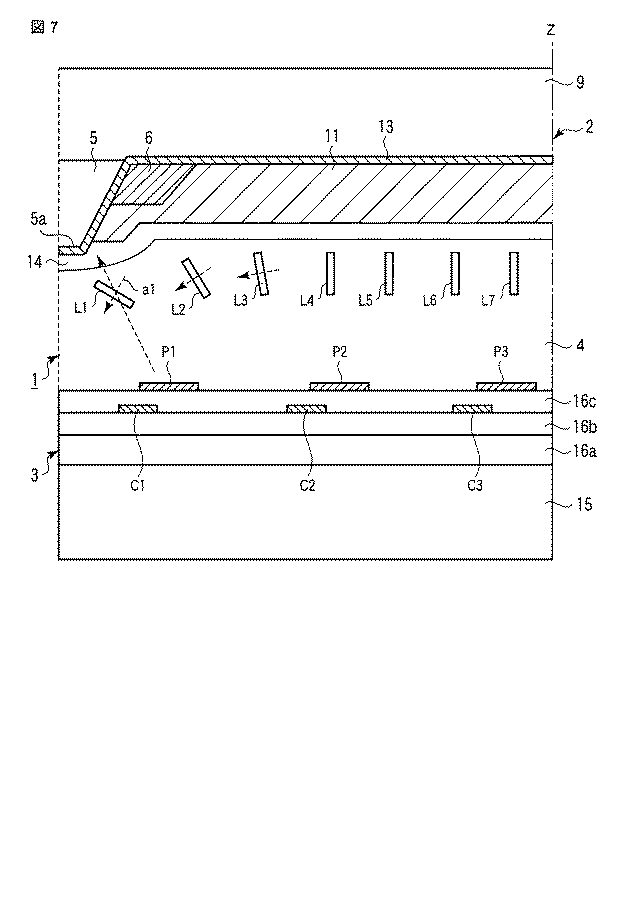
本実施形態においては、上記各実施形態で説明された液晶表示装置1又は液晶表示装置18の視野角制御の作用について説明する。なお、本実施形態では、上記図1に示す液晶表示用基板2を備える液晶表示装置1について説明するが、液晶表示用基板2Aを備える液晶表示装置1又は液晶表示装置18についても同様である。
本実施形態においては、上記各実施形態で説明された液晶表示装置1又は液晶表示装置18の変形例について説明する。なお、なお、本実施形態では、上記図1に示す液晶表示用基板2を備える液晶表示装置1の変形例について説明するが、液晶表示用基板2Aを備える液晶表示装置1又は液晶表示装置18についても同様に変形可能である。
Claims (14)
- 液晶表示用基板と、当該液晶表示用基板に液晶層を挟んで対向し、かつ、メタル配線を備えたアレイ基板とを具備する液晶表示装置に用いられる液晶表示用基板であって、
平面形状において向かい合い、かつ、前記メタル配線と平行な辺を持つ多角形画素又は多角形サブピクセルと、
前記多角形画素又は前記多角形サブピクセルの前記向かい合う平行な辺に備えられ、基板面の垂直方向で前記メタル配線と対向し、斜め光を透過する線状パターンと
を具備する液晶表示用基板。 - 前記線状パターンは、平面形状において、線状の透明パターンを線状の遮光パターンで挟む構成を持ち、
前記斜め光の角度は、前記透明パターンの幅、前記線状パターンの幅、前記透明パターンの厚さ、前記透明パターンと前記液晶表示用基板の保護層との厚さ、前記液晶層の厚さ、前記液晶層のうちの前記透明パターンの表面に近い液晶のチルト角のうちの少なくとも一つとともに前記メタル配線の幅により制御される、請求項1記載の液晶表示用基板。 - 前記線状パターンは、平面形状において、前記透明パターンの中央、かつ、線状の長手方向に遮光部をさらに具備する、請求項2記載の液晶表示用基板。
- 前記線状パターン上に形成される透明導電膜をさらに具備する、請求項1乃至請求項3のいずれか1項に記載の液晶表示用基板。
- 一方の表面上に前記線状パターンが形成されている透明基板と、
前記線状パターンが形成されている前記透明基板の前記表面に積層される透明導電膜と、
前記透明導電膜上に形成される前記多角形画素又は前記多角形サブピクセルのカラーフィルタと
を具備する請求項1記載の液晶表示用基板。 - 前記カラーフィルタとして、少なくとも赤カラーフィルタ、緑カラーフィルタ、青カラーフィルタのうちの2以上が用いられる、請求項5記載の液晶表示用基板。
- 前記多角形画素又は前記多角形サブピクセルの前記平面形状は、長方形、平行四辺形、くの字状に折れ曲がった多角形のうちのいずれかである、請求項1乃至請求項6のいずれか1項に記載の液晶表示用基板。
- 前記透明パターンの形成部分は、前記他の部分よりも厚いことを特徴とする請求項1乃至請求項7のいずれか1項に記載の液晶表用基板。
- 液晶表示用基板と、当該液晶表示用基板に液晶層を挟んで対向し、かつ、メタル配線を備えたアレイ基板とを具備する液晶表示装置であって、
前記液晶表示用基板は、平面形状において向かい合い、かつ、前記メタル配線と平行な辺を持つ多角形画素又は多角形サブピクセルと、前記多角形画素又は前記多角形サブピクセルの前記向かい合う平行な辺に備えられ、基板面の垂直方向で前記メタル配線と対向し、斜め光を透過する線状パターンとを具備し、
前記アレイ基板は、前記液晶層の液晶を駆動するアクティブ素子を備える
ことを具備する液晶表示装置。 - 前記アレイ基板は、前記多角形画素又は前記多角形サブピクセルごとに、前記液晶を駆動するために異なる電位が印加される第1電極と第2電極とを具備し、
前記線状パターンは、平面形状において、線状の透明パターンを線状の遮光パターンで挟む構成を持ち、
前記斜め光の角度は、前記透明パターンの幅、前記線状パターンの幅、前記透明パターンの厚さ、前記透明パターンと前記液晶表示用基板の保護層との厚さ、前記液晶層の厚さ、前記液晶層のうちの前記透明パターンの表面に近い液晶のチルト角のうちの少なくとも一つとともに前記メタル配線の幅により制御される、請求項9記載の液晶表示装置。 - 前記第1電極は、前記液晶を駆動するアクティブ素子と接続された第1の櫛歯状パターンであり、
前記第2電極は、絶縁層を介して前記第1電極の下に配設された第2の櫛歯状パターンであり、水平方向において、前記多角形画素又は前記多角形サブマトリクスを垂直方向に2分する中心軸の反対方向に、前記第1電極の端部からはみ出た位置に配置されることを特徴とする請求項10記載の液晶表示装置。 - 前記多角形画素又は前記多角形サブマトリクスごとに、2以上の前記アクティブ素子を備えており、
前記多角形画素又は前記多角形サブマトリクスごとに備えられている前記2以上のアクティブ素子は、前記多角形画素又は前記多角形サブマトリクスごとに、前記第1電極における電気的に独立の2以上の部分に、それぞれ接続される
ことを特徴とする請求項10又は請求項11記載の液晶表示装置。 - 前記第1電極及び前記第2電極は、可視域で透明な導電性金属酸化物によって形成される、請求項10乃至請求項12のいずれか1項に記載の液晶表示装置。
- 前記液晶は負の誘電率異方性を有する、請求項9乃至請求項13のいずれか1項に記載の液晶表示装置。
Priority Applications (7)
| Application Number | Priority Date | Filing Date | Title |
|---|---|---|---|
| JP2011019833A JP5152352B2 (ja) | 2011-02-01 | 2011-02-01 | 液晶表示用基板及び液晶表示装置 |
| CN2011800666290A CN103339557A (zh) | 2011-02-01 | 2011-05-24 | 液晶显示用基板及液晶显示装置 |
| PCT/JP2011/061876 WO2012105067A1 (ja) | 2011-02-01 | 2011-05-24 | 液晶表示用基板及び液晶表示装置 |
| EP11857471.4A EP2672315A4 (en) | 2011-02-01 | 2011-05-24 | Liquid crystal display substrate and liquid crystal display device |
| KR1020137020363A KR20140008338A (ko) | 2011-02-01 | 2011-05-24 | 액정 표시용 기판 및 액정 표시 장치 |
| TW100124860A TWI467279B (zh) | 2011-02-01 | 2011-07-14 | 液晶顯示用基板及液晶顯示裝置 |
| US13/946,737 US20130300989A1 (en) | 2011-02-01 | 2013-07-19 | Substrate for liquid crystal display and liquid crystal display device |
Applications Claiming Priority (1)
| Application Number | Priority Date | Filing Date | Title |
|---|---|---|---|
| JP2011019833A JP5152352B2 (ja) | 2011-02-01 | 2011-02-01 | 液晶表示用基板及び液晶表示装置 |
Publications (2)
| Publication Number | Publication Date |
|---|---|
| JP2012159729A JP2012159729A (ja) | 2012-08-23 |
| JP5152352B2 true JP5152352B2 (ja) | 2013-02-27 |
Family
ID=46602304
Family Applications (1)
| Application Number | Title | Priority Date | Filing Date |
|---|---|---|---|
| JP2011019833A Expired - Fee Related JP5152352B2 (ja) | 2011-02-01 | 2011-02-01 | 液晶表示用基板及び液晶表示装置 |
Country Status (7)
| Country | Link |
|---|---|
| US (1) | US20130300989A1 (ja) |
| EP (1) | EP2672315A4 (ja) |
| JP (1) | JP5152352B2 (ja) |
| KR (1) | KR20140008338A (ja) |
| CN (1) | CN103339557A (ja) |
| TW (1) | TWI467279B (ja) |
| WO (1) | WO2012105067A1 (ja) |
Families Citing this family (17)
| Publication number | Priority date | Publication date | Assignee | Title |
|---|---|---|---|---|
| TWI485490B (zh) * | 2012-09-04 | 2015-05-21 | Au Optronics Corp | 防窺顯示裝置及其驅動方法 |
| TWI476495B (zh) * | 2012-09-26 | 2015-03-11 | Au Optronics Corp | 具有位置資訊之顯示器 |
| WO2014103777A1 (ja) * | 2012-12-27 | 2014-07-03 | 凸版印刷株式会社 | 液晶表示装置、液晶表示装置用基板、及び液晶表示装置用基板の製造方法 |
| CN103268042B (zh) * | 2013-05-20 | 2015-11-25 | 昆山龙腾光电有限公司 | 液晶显示装置 |
| CN105308499B (zh) * | 2013-06-28 | 2017-08-29 | 夏普株式会社 | 液晶显示装置 |
| KR102150080B1 (ko) * | 2013-09-12 | 2020-09-01 | 삼성디스플레이 주식회사 | 표시 패널 및 이를 포함하는 표시 장치 |
| JP2015090435A (ja) * | 2013-11-06 | 2015-05-11 | 株式会社ジャパンディスプレイ | 液晶表示装置 |
| CN104932167B (zh) * | 2015-06-25 | 2018-06-19 | 深圳市华星光电技术有限公司 | 蓝相液晶显示装置及其驱动方法 |
| JP6848043B2 (ja) | 2016-08-08 | 2021-03-24 | 昆山龍騰光電有限公司 | 視野角切替可能な液晶表示装置及びその視野角切替方法 |
| KR102716926B1 (ko) | 2016-12-26 | 2024-10-11 | 엘지디스플레이 주식회사 | 터치 스크린 일체형 표시장치 |
| CN106814506B (zh) * | 2017-04-01 | 2018-09-04 | 深圳市华星光电技术有限公司 | 一种液晶显示面板及装置 |
| CN107843993B (zh) * | 2017-11-09 | 2020-01-10 | 维沃移动通信有限公司 | 一种显示屏可视角度的控制方法、移动终端及计算机存储介质 |
| JP2019090954A (ja) * | 2017-11-16 | 2019-06-13 | シャープ株式会社 | カラーフィルタ基板及びその製造方法、並びに表示パネル |
| CN108549166B (zh) * | 2018-04-17 | 2021-11-02 | 京东方科技集团股份有限公司 | 防窥子像素单元及其制作方法以及显示装置及其驱动方法 |
| CN110376773B (zh) * | 2019-07-22 | 2022-02-11 | 昆山龙腾光电股份有限公司 | 视角可切换液晶显示装置的驱动方法 |
| CN110456580B (zh) * | 2019-08-26 | 2022-04-29 | 京东方科技集团股份有限公司 | 一种显示基板及其控制方法、显示面板、显示装置 |
| CN114326199B (zh) * | 2021-12-31 | 2024-04-02 | 厦门天马微电子有限公司 | 显示面板和显示装置 |
Family Cites Families (15)
| Publication number | Priority date | Publication date | Assignee | Title |
|---|---|---|---|---|
| JP3322197B2 (ja) | 1997-12-17 | 2002-09-09 | 松下電器産業株式会社 | 液晶表示装置 |
| JP2001324710A (ja) * | 2000-05-17 | 2001-11-22 | Nec Corp | 液晶表示装置およびその製造方法ならびに駆動方法 |
| JP4226503B2 (ja) * | 2004-03-23 | 2009-02-18 | シャープ株式会社 | 液晶表示装置および電子機器 |
| JP4367206B2 (ja) | 2004-04-01 | 2009-11-18 | セイコーエプソン株式会社 | 視角制御素子、液晶表示装置、電子機器 |
| JP2006309105A (ja) * | 2005-03-30 | 2006-11-09 | Casio Comput Co Ltd | 液晶表示素子 |
| KR20060106168A (ko) * | 2005-04-06 | 2006-10-12 | 삼성전자주식회사 | 액정표시장치 |
| JP5168767B2 (ja) | 2005-08-29 | 2013-03-27 | カシオ計算機株式会社 | 液晶表示装置 |
| KR101180718B1 (ko) * | 2005-12-29 | 2012-09-07 | 엘지디스플레이 주식회사 | 횡전계형 액정표시장치용 어레이 기판 및 그 제조 방법 |
| JP5061505B2 (ja) * | 2006-05-25 | 2012-10-31 | 日本電気株式会社 | 横電界方式のアクティブマトリクス型液晶表示装置 |
| KR101268954B1 (ko) * | 2006-06-29 | 2013-05-30 | 엘지디스플레이 주식회사 | 시야각 제어가 가능한 액정 표시 장치 및 그의 제조 방법 |
| KR20080111939A (ko) * | 2007-06-20 | 2008-12-24 | 엘지디스플레이 주식회사 | 액정 표시 장치 |
| KR100914785B1 (ko) * | 2007-12-26 | 2009-08-31 | 엘지디스플레이 주식회사 | 액정표시장치 |
| JP5301251B2 (ja) * | 2008-11-27 | 2013-09-25 | 株式会社ジャパンディスプレイウェスト | 液晶表示装置 |
| JP2009105424A (ja) | 2008-12-12 | 2009-05-14 | Kobe Steel Ltd | 薄膜トランジスタ基板および表示デバイス |
| JP5477686B2 (ja) * | 2009-03-25 | 2014-04-23 | 株式会社ジャパンディスプレイ | 電気光学装置および電子機器 |
-
2011
- 2011-02-01 JP JP2011019833A patent/JP5152352B2/ja not_active Expired - Fee Related
- 2011-05-24 KR KR1020137020363A patent/KR20140008338A/ko not_active Withdrawn
- 2011-05-24 WO PCT/JP2011/061876 patent/WO2012105067A1/ja not_active Ceased
- 2011-05-24 EP EP11857471.4A patent/EP2672315A4/en not_active Withdrawn
- 2011-05-24 CN CN2011800666290A patent/CN103339557A/zh active Pending
- 2011-07-14 TW TW100124860A patent/TWI467279B/zh not_active IP Right Cessation
-
2013
- 2013-07-19 US US13/946,737 patent/US20130300989A1/en not_active Abandoned
Also Published As
| Publication number | Publication date |
|---|---|
| EP2672315A1 (en) | 2013-12-11 |
| US20130300989A1 (en) | 2013-11-14 |
| CN103339557A (zh) | 2013-10-02 |
| JP2012159729A (ja) | 2012-08-23 |
| EP2672315A4 (en) | 2014-07-30 |
| TWI467279B (zh) | 2015-01-01 |
| WO2012105067A1 (ja) | 2012-08-09 |
| TW201234082A (en) | 2012-08-16 |
| KR20140008338A (ko) | 2014-01-21 |
Similar Documents
| Publication | Publication Date | Title |
|---|---|---|
| JP5152352B2 (ja) | 液晶表示用基板及び液晶表示装置 | |
| JP5578132B2 (ja) | 液晶表示装置 | |
| TWI464489B (zh) | 彩色濾光片基板及液晶顯示裝置 | |
| CN102918451B (zh) | 液晶显示装置 | |
| JP5659768B2 (ja) | 斜め電界液晶表示装置 | |
| JP5083467B2 (ja) | 液晶表示装置用カラーフィルタ基板および液晶表示装置 | |
| KR101822691B1 (ko) | 액정 표시 기판 및 액정 표시 장치 | |
| TWI470317B (zh) | 半透過型液晶顯示裝置用基板、彩色濾光片基板及液晶顯示裝置 | |
| JP5609791B2 (ja) | 液晶表示用の対向基板及び液晶表示装置 | |
| JP5158133B2 (ja) | 垂直配向液晶表示装置用基板および垂直配向液晶表示装置 | |
| JP5099174B2 (ja) | 垂直配向液晶表示装置用カラーフィルタ基板および垂直配向液晶表示装置 |
Legal Events
| Date | Code | Title | Description |
|---|---|---|---|
| A131 | Notification of reasons for refusal |
Free format text: JAPANESE INTERMEDIATE CODE: A131 Effective date: 20120821 |
|
| A521 | Written amendment |
Free format text: JAPANESE INTERMEDIATE CODE: A523 Effective date: 20121015 |
|
| TRDD | Decision of grant or rejection written | ||
| A01 | Written decision to grant a patent or to grant a registration (utility model) |
Free format text: JAPANESE INTERMEDIATE CODE: A01 Effective date: 20121106 |
|
| A61 | First payment of annual fees (during grant procedure) |
Free format text: JAPANESE INTERMEDIATE CODE: A61 Effective date: 20121119 |
|
| FPAY | Renewal fee payment (event date is renewal date of database) |
Free format text: PAYMENT UNTIL: 20151214 Year of fee payment: 3 |
|
| R150 | Certificate of patent or registration of utility model |
Ref document number: 5152352 Country of ref document: JP Free format text: JAPANESE INTERMEDIATE CODE: R150 Free format text: JAPANESE INTERMEDIATE CODE: R150 |
|
| LAPS | Cancellation because of no payment of annual fees |