JP5157268B2 - スピン蓄積磁化反転型のメモリ素子及びスピンram - Google Patents
スピン蓄積磁化反転型のメモリ素子及びスピンram Download PDFInfo
- Publication number
- JP5157268B2 JP5157268B2 JP2007155854A JP2007155854A JP5157268B2 JP 5157268 B2 JP5157268 B2 JP 5157268B2 JP 2007155854 A JP2007155854 A JP 2007155854A JP 2007155854 A JP2007155854 A JP 2007155854A JP 5157268 B2 JP5157268 B2 JP 5157268B2
- Authority
- JP
- Japan
- Prior art keywords
- ferromagnetic
- word line
- bit line
- nonmagnetic
- spin
- Prior art date
- Legal status (The legal status is an assumption and is not a legal conclusion. Google has not performed a legal analysis and makes no representation as to the accuracy of the status listed.)
- Expired - Fee Related
Links
Images





Classifications
-
- G—PHYSICS
- G11—INFORMATION STORAGE
- G11C—STATIC STORES
- G11C11/00—Digital stores characterised by the use of particular electric or magnetic storage elements; Storage elements therefor
- G11C11/02—Digital stores characterised by the use of particular electric or magnetic storage elements; Storage elements therefor using magnetic elements
- G11C11/16—Digital stores characterised by the use of particular electric or magnetic storage elements; Storage elements therefor using magnetic elements using elements in which the storage effect is based on magnetic spin effect
-
- G—PHYSICS
- G11—INFORMATION STORAGE
- G11C—STATIC STORES
- G11C11/00—Digital stores characterised by the use of particular electric or magnetic storage elements; Storage elements therefor
- G11C11/02—Digital stores characterised by the use of particular electric or magnetic storage elements; Storage elements therefor using magnetic elements
- G11C11/14—Digital stores characterised by the use of particular electric or magnetic storage elements; Storage elements therefor using magnetic elements using thin-film elements
- G11C11/15—Digital stores characterised by the use of particular electric or magnetic storage elements; Storage elements therefor using magnetic elements using thin-film elements using multiple magnetic layers
-
- G—PHYSICS
- G11—INFORMATION STORAGE
- G11C—STATIC STORES
- G11C11/00—Digital stores characterised by the use of particular electric or magnetic storage elements; Storage elements therefor
- G11C11/02—Digital stores characterised by the use of particular electric or magnetic storage elements; Storage elements therefor using magnetic elements
- G11C11/16—Digital stores characterised by the use of particular electric or magnetic storage elements; Storage elements therefor using magnetic elements using elements in which the storage effect is based on magnetic spin effect
- G11C11/161—Digital stores characterised by the use of particular electric or magnetic storage elements; Storage elements therefor using magnetic elements using elements in which the storage effect is based on magnetic spin effect details concerning the memory cell structure, e.g. the layers of the ferromagnetic memory cell
-
- G—PHYSICS
- G11—INFORMATION STORAGE
- G11C—STATIC STORES
- G11C11/00—Digital stores characterised by the use of particular electric or magnetic storage elements; Storage elements therefor
- G11C11/02—Digital stores characterised by the use of particular electric or magnetic storage elements; Storage elements therefor using magnetic elements
- G11C11/16—Digital stores characterised by the use of particular electric or magnetic storage elements; Storage elements therefor using magnetic elements using elements in which the storage effect is based on magnetic spin effect
- G11C11/165—Auxiliary circuits
- G11C11/1653—Address circuits or decoders
- G11C11/1657—Word-line or row circuits
-
- G—PHYSICS
- G11—INFORMATION STORAGE
- G11C—STATIC STORES
- G11C11/00—Digital stores characterised by the use of particular electric or magnetic storage elements; Storage elements therefor
- G11C11/02—Digital stores characterised by the use of particular electric or magnetic storage elements; Storage elements therefor using magnetic elements
- G11C11/16—Digital stores characterised by the use of particular electric or magnetic storage elements; Storage elements therefor using magnetic elements using elements in which the storage effect is based on magnetic spin effect
- G11C11/165—Auxiliary circuits
- G11C11/1659—Cell access
-
- G—PHYSICS
- G11—INFORMATION STORAGE
- G11C—STATIC STORES
- G11C11/00—Digital stores characterised by the use of particular electric or magnetic storage elements; Storage elements therefor
- G11C11/02—Digital stores characterised by the use of particular electric or magnetic storage elements; Storage elements therefor using magnetic elements
- G11C11/16—Digital stores characterised by the use of particular electric or magnetic storage elements; Storage elements therefor using magnetic elements using elements in which the storage effect is based on magnetic spin effect
- G11C11/165—Auxiliary circuits
- G11C11/1673—Reading or sensing circuits or methods
-
- G—PHYSICS
- G11—INFORMATION STORAGE
- G11C—STATIC STORES
- G11C11/00—Digital stores characterised by the use of particular electric or magnetic storage elements; Storage elements therefor
- G11C11/02—Digital stores characterised by the use of particular electric or magnetic storage elements; Storage elements therefor using magnetic elements
- G11C11/16—Digital stores characterised by the use of particular electric or magnetic storage elements; Storage elements therefor using magnetic elements using elements in which the storage effect is based on magnetic spin effect
- G11C11/165—Auxiliary circuits
- G11C11/1675—Writing or programming circuits or methods
-
- G—PHYSICS
- G11—INFORMATION STORAGE
- G11C—STATIC STORES
- G11C5/00—Details of stores covered by group G11C11/00
- G11C5/06—Arrangements for interconnecting storage elements electrically, e.g. by wiring
-
- H—ELECTRICITY
- H10—SEMICONDUCTOR DEVICES; ELECTRIC SOLID-STATE DEVICES NOT OTHERWISE PROVIDED FOR
- H10B—ELECTRONIC MEMORY DEVICES
- H10B61/00—Magnetic memory devices, e.g. magnetoresistive RAM [MRAM] devices
- H10B61/20—Magnetic memory devices, e.g. magnetoresistive RAM [MRAM] devices comprising components having three or more electrodes, e.g. transistors
- H10B61/22—Magnetic memory devices, e.g. magnetoresistive RAM [MRAM] devices comprising components having three or more electrodes, e.g. transistors of the field-effect transistor [FET] type
-
- H—ELECTRICITY
- H10—SEMICONDUCTOR DEVICES; ELECTRIC SOLID-STATE DEVICES NOT OTHERWISE PROVIDED FOR
- H10N—ELECTRIC SOLID-STATE DEVICES NOT OTHERWISE PROVIDED FOR
- H10N50/00—Galvanomagnetic devices
- H10N50/10—Magnetoresistive devices
Landscapes
- Engineering & Computer Science (AREA)
- Computer Hardware Design (AREA)
- Mram Or Spin Memory Techniques (AREA)
- Hall/Mr Elements (AREA)
Description
図1に、本発明を適用した磁気メモリを示す。この磁気メモリ100は、格子状に並べられた複数の強磁性書き込みワード線101と複数の非磁性ビット線102とを有する。強磁性書き込みワード線101と非磁性ビット線102とが交差する部分には、メモリ素子103が配置されている。メモリ素子103は金属配線層104を介してトランジスタ105のソース電極に接続されている。
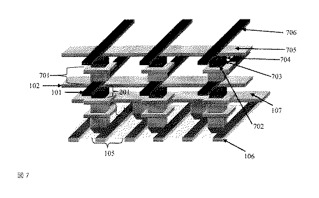
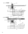
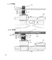
図5に示すように、非磁性ビット線102と強磁性書き込みワード線101とは、第2の絶縁層501を介して、電気的に接続されても良い。ここで、第2の絶縁層は、トンネルバリアとしての機能を持つ。
図6に示すように、第2の強磁性層と非磁性ビット線102とは、第3の絶縁層601を介して、電気的に接続されても良い。ここで、第3の絶縁層は、トンネルバリアとしての機能を持つ。第3の絶縁層を用いない場合、第2の強磁性層はスピン分極した電子のシンクとして作用する。一方、第3の絶縁層を用いた場合、電子は界面での散乱を受けないので高い分極率を保持したまま第2の強磁性層に伝導する。
スピン蓄積磁化反転型磁気記録素子を備えた磁気メモリにおいて、多値の構造を作製する場合の実施例を述べる。
Claims (12)
- 強磁性ワード線と、
前記強磁性ワード線と交差する非磁性ビット線と、
前記強磁性ワード線と対向する配線と、
前記強磁性ワード線及び前記非磁性ビット線の交差部分と前記配線との間に設けられた磁気抵抗効果素子とを備え、
前記磁気抵抗効果素子は、前記配線側に設けられた第1の強磁性層と、前記強磁性ワード線側に設けられた第2の強磁性層と、前記第1の強磁性層と前記第2の強磁性層との間に設けられた非磁性層とを有し、
書き込み動作時には、前記強磁性ワード線と前記非磁性ビット線との間に電流を流し、前記強磁性ワード線から前記非磁性ビット線にスピンを蓄積させることで前記第2の強磁性層の磁化方向を反転させ、
読み出し動作時には、前記磁気抵抗効果素子の膜厚方向に電流を流すことを特徴とするメモリ素子。 - 前記書き込み動作時において、
前記非磁性ビット線から前記強磁性ワード線に向かって電流を流すことにより、前記強磁性ワード線から前記非磁性ビット線にアップスピンを蓄積させ、
前記強磁性ワード線から非磁性ビット線に向かって電流を流すことにより、前記強磁性ワード線から非磁性ビット線にダウンスピンを蓄積させることを特徴とする請求項1記載のメモリ素子。 - 前記アップスピンが蓄積されることにより、前記第2の強磁性層の磁化方向は、前記強磁性ワードの磁化方向と平行になり、
前記ダウンスピンが蓄積されることにより、前記第2の強磁性層の磁化方向は、前記強磁性ワード線の磁化方向と反平行になることを特徴とする請求項2記載のメモリ素子。 - 前記読み出し動作時において、前記非磁性ビット線と前記配線との間に電流を流すことを特徴とする請求項1記載のメモリ素子。
- 前記磁気抵抗効果素子は、スイッチング素子を介してソース線に電気的に接続されることを特徴とする請求項4記載のメモリ素子。
- 前記スイッチング素子はトランジスタであり、
前記トランジスタのゲート電極に電気的に接続される読み出しワード線と、
前記トランジスタのドレイン電極に電気的に接続される前記ソース線と、
前記トランジスタのソース電極に電気的に接続される前記配線とを備えることを特徴とする請求項5記載のメモリ素子。 - 更に、前記非磁性ビット線と前記強磁性ワード線との間に設けられた絶縁層を有することを特徴とする請求項1記載のメモリ素子。
- 更に、前記第2の強磁性層と非磁性ビット線との間に設けられた絶縁層を有することを特徴とする請求項1記載のメモリ素子。
- 前記磁気抵抗効果素子は、CPP-GMR又はTMRであることを特徴とする請求項1記載のメモリ素子。
- 第1の強磁性ワード線と、
前記第1の強磁性ワード線と交差する第1の非磁性ビット線と、
前記第1の強磁性ワード線と対向する第1の配線と、
前記第1の強磁性ワード線及び前記第1の非磁性ビット線の交差部分と前記第1の配線との間に設けられた第1の磁気抵抗効果素子と、
前記第1の強磁性ワード線の前記第1非磁性ビット線と交差する面とは反対側に設けられた第2の配線と、
第2の強磁性ワード線と、
前記第2の強磁性ワード線と交差する第2の非磁性ビット線と、
前記第2の強磁性ワード線及び前記第2の非磁性ビット線の交差部分と前記第2の配線との間に設けられた第2の磁気抵抗効果素子とを備え、
前記第1の磁気抵抗効果素子は、前記第1の配線側に設けられた第1の強磁性層と、前記第1の強磁性ワード線側に設けられた第2の強磁性層と、前記第1の強磁性層と前記第2の強磁性層との間に設けられた第1の非磁性層とを有し、
前記第2の磁気抵抗効果素子は、前記第2の配線側に設けられた第3の強磁性層と、前記第2の強磁性ワード線側に設けられた第4の強磁性層と、前記第3の強磁性層と第4の強磁性層との間に設けられた第2の非磁性層とを有し、
書き込み動作時には、前記第1の強磁性ワード線と第1の非磁性ビット線との間に電流を流し、前記第1の強磁性ワード線から前記第1の非磁性ビット線にスピンを蓄積させることで前記第2の強磁性層の磁化方向を反転させ、
前記第2の強磁性ワード線と第2の非磁性ビット線との間に電流を流し、前記第2の強磁性ワード線から前記第2の非磁性ビット線にスピンを蓄積させることで第4の強磁性層の磁化方向を反転させ、
読み出し動作時には、前記第1の磁気抵抗効果素子及び第2の磁気抵抗効果素子の膜厚方向に電流を流すことを特徴とするスピンRAM。 - 前記第1の磁気抵抗効果素子及び第2の磁気抵抗効果素子は、スイッチング素子を介して、ソース線に電気的に接続されることを特徴とする請求項10記載のスピンRAM。
- 前記スイッチング素子はトランジスタであり、
前記トランジスタのゲート電極に電気的に接続される読み出しワード線と、
前記トランジスタのドレイン電極に電気的に接続される前記ソース線と、
前記トランジスタのソース電極に電気的に接続される前記第1の配線とを備えることを特徴とする請求項11記載のスピンRAM。
Priority Applications (5)
| Application Number | Priority Date | Filing Date | Title |
|---|---|---|---|
| JP2007155854A JP5157268B2 (ja) | 2007-06-13 | 2007-06-13 | スピン蓄積磁化反転型のメモリ素子及びスピンram |
| US12/149,827 US7613036B2 (en) | 2007-06-13 | 2008-05-08 | Memory element utilizing magnetization switching caused by spin accumulation and spin RAM device using the memory element |
| TW097117004A TWI391928B (zh) | 2007-06-13 | 2008-05-08 | 自旋累積磁化反轉型記憶體元件及自旋隨機存取記憶體 |
| CN2008100988627A CN101325087B (zh) | 2007-06-13 | 2008-05-19 | 自旋累积磁化反转型存储元件及自旋ram |
| KR1020080047648A KR100948727B1 (ko) | 2007-06-13 | 2008-05-22 | 스핀 축적 자화 반전형의 메모리 소자 및 스핀 ram |
Applications Claiming Priority (1)
| Application Number | Priority Date | Filing Date | Title |
|---|---|---|---|
| JP2007155854A JP5157268B2 (ja) | 2007-06-13 | 2007-06-13 | スピン蓄積磁化反転型のメモリ素子及びスピンram |
Publications (2)
| Publication Number | Publication Date |
|---|---|
| JP2008311321A JP2008311321A (ja) | 2008-12-25 |
| JP5157268B2 true JP5157268B2 (ja) | 2013-03-06 |
Family
ID=40132145
Family Applications (1)
| Application Number | Title | Priority Date | Filing Date |
|---|---|---|---|
| JP2007155854A Expired - Fee Related JP5157268B2 (ja) | 2007-06-13 | 2007-06-13 | スピン蓄積磁化反転型のメモリ素子及びスピンram |
Country Status (5)
| Country | Link |
|---|---|
| US (1) | US7613036B2 (ja) |
| JP (1) | JP5157268B2 (ja) |
| KR (1) | KR100948727B1 (ja) |
| CN (1) | CN101325087B (ja) |
| TW (1) | TWI391928B (ja) |
Families Citing this family (16)
| Publication number | Priority date | Publication date | Assignee | Title |
|---|---|---|---|---|
| JP2009158877A (ja) | 2007-12-28 | 2009-07-16 | Hitachi Ltd | 磁気メモリセル及びランダムアクセスメモリ |
| KR101598542B1 (ko) * | 2009-01-13 | 2016-02-29 | 삼성전자주식회사 | 스핀 전계효과 트랜지스터를 이용한 논리소자 |
| JP5318191B2 (ja) * | 2009-03-04 | 2013-10-16 | 株式会社日立製作所 | 磁気メモリ |
| KR101048351B1 (ko) * | 2009-06-08 | 2011-07-14 | 한양대학교 산학협력단 | 자성 메모리의 동작방법 |
| EP2453482A4 (en) * | 2009-07-09 | 2013-04-24 | Univ Kyushu Nat Univ Corp | MAGNETIZATION REVERSE DEVICE, MEMORY ELEMENT AND MAGNETIC FIELD GENERATING DEVICE |
| JP5379675B2 (ja) * | 2009-12-28 | 2013-12-25 | 株式会社日立製作所 | 磁気メモリセル及び磁気メモリ |
| US9047965B2 (en) | 2011-12-20 | 2015-06-02 | Everspin Technologies, Inc. | Circuit and method for spin-torque MRAM bit line and source line voltage regulation |
| JP5486048B2 (ja) * | 2012-06-26 | 2014-05-07 | 株式会社日立製作所 | 磁気メモリセル及びランダムアクセスメモリ |
| KR101266791B1 (ko) * | 2012-09-21 | 2013-05-27 | 고려대학교 산학협력단 | 면내 전류와 전기장을 이용한 자기메모리 소자 |
| US10403766B2 (en) | 2012-12-04 | 2019-09-03 | Conversant Intellectual Property Management Inc. | NAND flash memory with vertical cell stack structure and method for manufacturing same |
| CN105242094A (zh) * | 2015-11-11 | 2016-01-13 | 电子科技大学 | 一种fm/nm薄膜结构中逆自旋霍尔电压值的测量方法 |
| JP7023637B2 (ja) * | 2017-08-08 | 2022-02-22 | 株式会社日立ハイテク | 磁気トンネル接合素子の製造方法 |
| US10134457B1 (en) * | 2017-08-31 | 2018-11-20 | Sandisk Technologies Llc | Cross-point spin accumulation torque MRAM |
| CN109285577B (zh) * | 2018-08-31 | 2021-07-30 | 北京大学(天津滨海)新一代信息技术研究院 | 一种基于分子自旋态的超低功耗存储器件及数据存储方法 |
| CN110890458B (zh) * | 2018-09-07 | 2024-04-12 | 上海磁宇信息科技有限公司 | 一种提高磁性随机存储器写入效率的方法 |
| CN109638151B (zh) * | 2018-12-04 | 2020-07-31 | 中国科学院上海微系统与信息技术研究所 | 存储单元、低温存储器及其读写方法 |
Family Cites Families (17)
| Publication number | Priority date | Publication date | Assignee | Title |
|---|---|---|---|---|
| US6611405B1 (en) * | 1999-09-16 | 2003-08-26 | Kabushiki Kaisha Toshiba | Magnetoresistive element and magnetic memory device |
| TW503393B (en) * | 2001-03-28 | 2002-09-21 | United Microelectronics Corp | Magneto-resistance random access memory array having pseudo spin valve |
| JP2003197875A (ja) * | 2001-12-28 | 2003-07-11 | Toshiba Corp | 磁気記憶装置 |
| JP4157707B2 (ja) * | 2002-01-16 | 2008-10-01 | 株式会社東芝 | 磁気メモリ |
| SG115462A1 (en) * | 2002-03-12 | 2005-10-28 | Inst Data Storage | Multi-stage per cell magnetoresistive random access memory |
| US6778421B2 (en) * | 2002-03-14 | 2004-08-17 | Hewlett-Packard Development Company, Lp. | Memory device array having a pair of magnetic bits sharing a common conductor line |
| US6879512B2 (en) * | 2002-05-24 | 2005-04-12 | International Business Machines Corporation | Nonvolatile memory device utilizing spin-valve-type designs and current pulses |
| JP4477305B2 (ja) * | 2002-07-25 | 2010-06-09 | 独立行政法人科学技術振興機構 | スピントランジスタ及びそれを用いた不揮発性メモリ |
| JP3818276B2 (ja) * | 2003-06-24 | 2006-09-06 | 独立行政法人科学技術振興機構 | スピン注入素子及びそれを用いた磁気装置 |
| JP2005064050A (ja) * | 2003-08-14 | 2005-03-10 | Toshiba Corp | 半導体記憶装置及びそのデータ書き込み方法 |
| KR100835275B1 (ko) * | 2004-08-12 | 2008-06-05 | 삼성전자주식회사 | 스핀 주입 메카니즘을 사용하여 자기램 소자를 구동시키는방법들 |
| US7009877B1 (en) * | 2003-11-14 | 2006-03-07 | Grandis, Inc. | Three-terminal magnetostatically coupled spin transfer-based MRAM cell |
| US7088609B2 (en) * | 2004-05-11 | 2006-08-08 | Grandis, Inc. | Spin barrier enhanced magnetoresistance effect element and magnetic memory using the same |
| JP2006237329A (ja) * | 2005-02-25 | 2006-09-07 | Toshiba Corp | 磁気記憶装置及び磁気記憶装置の書き込み方法 |
| US7286395B2 (en) * | 2005-10-27 | 2007-10-23 | Grandis, Inc. | Current driven switched magnetic storage cells having improved read and write margins and magnetic memories using such cells |
| JP4997789B2 (ja) * | 2006-02-23 | 2012-08-08 | Tdk株式会社 | 磁気メモリ |
| JP5034318B2 (ja) * | 2006-05-24 | 2012-09-26 | Tdk株式会社 | 磁気メモリ |
-
2007
- 2007-06-13 JP JP2007155854A patent/JP5157268B2/ja not_active Expired - Fee Related
-
2008
- 2008-05-08 TW TW097117004A patent/TWI391928B/zh active
- 2008-05-08 US US12/149,827 patent/US7613036B2/en not_active Expired - Fee Related
- 2008-05-19 CN CN2008100988627A patent/CN101325087B/zh not_active Expired - Fee Related
- 2008-05-22 KR KR1020080047648A patent/KR100948727B1/ko not_active Expired - Fee Related
Also Published As
| Publication number | Publication date |
|---|---|
| US7613036B2 (en) | 2009-11-03 |
| CN101325087A (zh) | 2008-12-17 |
| KR100948727B1 (ko) | 2010-03-22 |
| US20080310216A1 (en) | 2008-12-18 |
| JP2008311321A (ja) | 2008-12-25 |
| KR20080109611A (ko) | 2008-12-17 |
| CN101325087B (zh) | 2012-07-25 |
| TW200912925A (en) | 2009-03-16 |
| TWI391928B (zh) | 2013-04-01 |
Similar Documents
| Publication | Publication Date | Title |
|---|---|---|
| JP5157268B2 (ja) | スピン蓄積磁化反転型のメモリ素子及びスピンram | |
| Kawahara et al. | Spin-transfer torque RAM technology: Review and prospect | |
| CN101689600B (zh) | 磁阻效应元件及磁性随机存取存储器 | |
| CN102403029B (zh) | 存储元件和存储装置 | |
| JP6290487B1 (ja) | 磁気メモリ | |
| JP5260040B2 (ja) | 単一方向電流磁化反転磁気抵抗効果素子と磁気記録装置 | |
| JP5370907B2 (ja) | 磁気抵抗効果素子、及び磁気ランダムアクセスメモリ | |
| JP6495980B2 (ja) | 磁気メモリ | |
| JP6617829B2 (ja) | 磁壁利用型スピンmosfet、磁壁利用型アナログメモリ、不揮発性ロジック回路および磁気ニューロ素子 | |
| JP6861996B2 (ja) | 磁気抵抗効果素子及び磁気メモリ装置 | |
| TW201836071A (zh) | 磁性記憶體裝置 | |
| JP2006303159A (ja) | スピン注入磁区移動素子およびこれを用いた装置 | |
| TW201705565A (zh) | 磁阻效應元件及磁性記憶體 | |
| CN102403026A (zh) | 存储元件和存储装置 | |
| JPWO2012160937A1 (ja) | 磁気メモリ素子および磁気メモリ | |
| US10902987B2 (en) | Spin-orbit torque type magnetization rotation element, spin-orbit torque magnetoresistance effect element, and method of manufacturing spin-orbit torque type magnetization rotation element | |
| JP2008187048A (ja) | 磁気抵抗効果素子 | |
| JP2010098259A (ja) | メモリセル、ならびに、磁気メモリ素子 | |
| JP2013115412A (ja) | 記憶素子、記憶装置 | |
| JP3833990B2 (ja) | 磁気抵抗効果素子および磁気メモリ装置 | |
| JP5625380B2 (ja) | 磁気抵抗記憶素子及び磁気ランダムアクセスメモリ | |
| JP5382295B2 (ja) | 磁気ランダムアクセスメモリ | |
| JP2007027197A (ja) | 記憶素子 | |
| WO2012137911A1 (ja) | 磁気抵抗効果素子、及び磁気ランダムアクセスメモリ | |
| JP2013168667A (ja) | 磁気抵抗効果素子及びmram |
Legal Events
| Date | Code | Title | Description |
|---|---|---|---|
| A621 | Written request for application examination |
Free format text: JAPANESE INTERMEDIATE CODE: A621 Effective date: 20100312 |
|
| A977 | Report on retrieval |
Free format text: JAPANESE INTERMEDIATE CODE: A971007 Effective date: 20121102 |
|
| TRDD | Decision of grant or rejection written | ||
| A01 | Written decision to grant a patent or to grant a registration (utility model) |
Free format text: JAPANESE INTERMEDIATE CODE: A01 Effective date: 20121113 |
|
| A61 | First payment of annual fees (during grant procedure) |
Free format text: JAPANESE INTERMEDIATE CODE: A61 Effective date: 20121126 |
|
| FPAY | Renewal fee payment (event date is renewal date of database) |
Free format text: PAYMENT UNTIL: 20151221 Year of fee payment: 3 |
|
| LAPS | Cancellation because of no payment of annual fees |