JP5223635B2 - 半導体装置 - Google Patents
半導体装置 Download PDFInfo
- Publication number
- JP5223635B2 JP5223635B2 JP2008309828A JP2008309828A JP5223635B2 JP 5223635 B2 JP5223635 B2 JP 5223635B2 JP 2008309828 A JP2008309828 A JP 2008309828A JP 2008309828 A JP2008309828 A JP 2008309828A JP 5223635 B2 JP5223635 B2 JP 5223635B2
- Authority
- JP
- Japan
- Prior art keywords
- wiring
- terminal
- terminals
- power supply
- speed signal
- Prior art date
- Legal status (The legal status is an assumption and is not a legal conclusion. Google has not performed a legal analysis and makes no representation as to the accuracy of the status listed.)
- Expired - Fee Related
Links
Images




Classifications
-
- H—ELECTRICITY
- H10—SEMICONDUCTOR DEVICES; ELECTRIC SOLID-STATE DEVICES NOT OTHERWISE PROVIDED FOR
- H10W—GENERIC PACKAGES, INTERCONNECTIONS, CONNECTORS OR OTHER CONSTRUCTIONAL DETAILS OF DEVICES COVERED BY CLASS H10
- H10W72/00—Interconnections or connectors in packages
- H10W72/50—Bond wires
- H10W72/541—Dispositions of bond wires
- H10W72/5445—Dispositions of bond wires being orthogonal to a side surface of the chip, e.g. parallel arrangements
-
- H—ELECTRICITY
- H10—SEMICONDUCTOR DEVICES; ELECTRIC SOLID-STATE DEVICES NOT OTHERWISE PROVIDED FOR
- H10W—GENERIC PACKAGES, INTERCONNECTIONS, CONNECTORS OR OTHER CONSTRUCTIONAL DETAILS OF DEVICES COVERED BY CLASS H10
- H10W72/00—Interconnections or connectors in packages
- H10W72/50—Bond wires
- H10W72/541—Dispositions of bond wires
- H10W72/5449—Dispositions of bond wires not being orthogonal to a side surface of the chip, e.g. fan-out arrangements
-
- H—ELECTRICITY
- H10—SEMICONDUCTOR DEVICES; ELECTRIC SOLID-STATE DEVICES NOT OTHERWISE PROVIDED FOR
- H10W—GENERIC PACKAGES, INTERCONNECTIONS, CONNECTORS OR OTHER CONSTRUCTIONAL DETAILS OF DEVICES COVERED BY CLASS H10
- H10W72/00—Interconnections or connectors in packages
- H10W72/90—Bond pads, in general
- H10W72/931—Shapes of bond pads
- H10W72/932—Plan-view shape, i.e. in top view
Landscapes
- Semiconductor Integrated Circuits (AREA)
Description
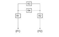
本発明の目的は、半導体パッケージの端子数の増加を抑制しながらも信号に対するノイズの影響を低減できるようにすることである。
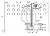
なお、図1(B)に示した例では、ボンディングパッド17に対して、ボンディングパッド17A、17Bをダイ11側に配置しているが、ダイ11に対する距離を同じにして、すべてのボンディングパッド17を配置するようにしても良い。図1(B)に示すように配置した場合には、ボンディングパッドの間隔を広げなくともガードリングGLを通すことができる。
本発明の諸態様を付記として以下に示す。
半導体ダイと、前記半導体ダイが搭載された基板とを有し、
前記基板は、
外部と信号を伝送する信号端子と、
外部より電源が供給される電源端子と、
前記半導体ダイに配置されている複数のパッドとワイヤで接続された複数のボンディングパッドと、
所定の信号を伝送する前記信号端子、当該信号端子に対応する前記ボンディングパッド、及び当該信号端子と当該ボンディングパッドとを接続する第1の配線を囲み、かつ前記電源端子に接続された第2の配線とを有することを特徴とする半導体装置。
(付記2)
前記第2の配線は、1つの前記電源端子に接続されていることを特徴とする付記1記載の半導体装置。
(付記3)
複数の前記第2の配線が、当該第2の配線の数よりも少ない数の前記電源端子にともに接続されていることを特徴とする付記1記載の半導体装置。
(付記4)
前記第2の配線は、接続された前記電源端子に対する経路及び距離の少なくとも一方に応じて配線幅が異なることを特徴とする付記1〜3の何れか1項に記載の半導体装置。
(付記5)
前記第2の配線は、接続された前記電源端子に対する距離の増加に伴って単位長さあたりの抵抗値が減少することを特徴とする付記1〜3の何れか1項に記載の半導体装置。
(付記6)
前記第2の配線は、接続された前記電源端子に対する距離の増加に伴って配線幅が太くなることを特徴とする付記1〜3の何れか1項に記載の半導体装置。
(付記7)
前記第2の配線は、接続された前記電源端子に対して遠い側の配線幅が、当該電源端子に対して近い側の配線幅より太いことを特徴とする付記1〜3の何れか1項に記載の半導体装置。
(付記8)
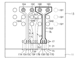
前記所定の信号を伝送する前記信号端子が隣接して配置され、隣接して配置された前記信号端子の間で一部を共用して、各々の前記信号端子に対応する前記第2の配線が形成されていることを特徴とする付記1〜7の何れか1項に記載の半導体装置。
(付記9)
前記所定の信号は差動信号であって、当該差動信号を伝送する1組の前記信号端子、当該1組の信号端子に対応する1組の前記ボンディングパッド、及び当該信号端子と当該ボンディングパッドとを接続する第1の配線を囲み、前記第2の配線が形成されていることを特徴とする付記1〜8の何れか1項に記載の半導体装置。
13 基板
15 パッド
17 ボンディングパッド
19 端子
19A〜19D 信号端子
19P 電源端子
21 ボンディングワイヤ
23 インターポーザ
GL シールド用配線(ガードリング)
Claims (4)
- 半導体ダイと、前記半導体ダイが搭載された基板とを有し、
前記基板は、
複数の信号端子と、
外部より電源が供給される複数の電源端子と、
前記半導体ダイに配置されている複数の端子と接続された複数のパッドと、
前記複数の信号端子の内の第1の信号端子と前記複数のパッドの内の第1のパッドとを接続する第1の配線と、
前記第1の信号端子と前記第1のパッドと前記第1の配線とを囲み、前記複数の電源端子の内の一つに接続された第2の配線とを有し、
前記第2の配線は、前記複数の電源端子の内の一つとの接続部分に対して近い側の配線幅よりも前記接続部分に対して遠い側の配線幅が太いことを特徴とする半導体装置。 - 前記第2の配線は、前記複数の電源端子の内の一つとの接続部分に対する距離の増加に伴って単位長さあたりの抵抗値が減少することを特徴とする請求項1に記載の半導体装置。
- 前記第1の信号端子と隣接して配置される前記複数の信号端子の内の第2の信号端子と、
前記複数のパッドの内の第2のパッドと、
前記第2の信号端子と前記第2のパッドとを接続する第3の配線と、
前記第2の信号端子と前記第2のパッドと前記第3の配線とを囲み、前記第2の配線と一部を共用する第4の配線とを有することを特徴とする請求項1又は2に記載の半導体装置。 - 前記第4の配線は、前記複数の電源端子の内の一つとの接続部分に対して近い側の配線幅よりも前記接続部分に対して遠い側の配線幅が太いことを特徴とする請求項3に記載の半導体装置。
Priority Applications (1)
| Application Number | Priority Date | Filing Date | Title |
|---|---|---|---|
| JP2008309828A JP5223635B2 (ja) | 2008-12-04 | 2008-12-04 | 半導体装置 |
Applications Claiming Priority (1)
| Application Number | Priority Date | Filing Date | Title |
|---|---|---|---|
| JP2008309828A JP5223635B2 (ja) | 2008-12-04 | 2008-12-04 | 半導体装置 |
Publications (2)
| Publication Number | Publication Date |
|---|---|
| JP2010135555A JP2010135555A (ja) | 2010-06-17 |
| JP5223635B2 true JP5223635B2 (ja) | 2013-06-26 |
Family
ID=42346549
Family Applications (1)
| Application Number | Title | Priority Date | Filing Date |
|---|---|---|---|
| JP2008309828A Expired - Fee Related JP5223635B2 (ja) | 2008-12-04 | 2008-12-04 | 半導体装置 |
Country Status (1)
| Country | Link |
|---|---|
| JP (1) | JP5223635B2 (ja) |
Cited By (1)
| Publication number | Priority date | Publication date | Assignee | Title |
|---|---|---|---|---|
| JPWO2015147058A1 (ja) * | 2014-03-27 | 2017-04-13 | シチズンファインデバイス株式会社 | 圧力検出装置 |
Families Citing this family (3)
| Publication number | Priority date | Publication date | Assignee | Title |
|---|---|---|---|---|
| JP5390494B2 (ja) * | 2010-09-14 | 2014-01-15 | ルネサスエレクトロニクス株式会社 | 半導体装置 |
| JP5764381B2 (ja) * | 2011-05-09 | 2015-08-19 | 新光電気工業株式会社 | 配線基板の検査方法、配線基板の製造方法 |
| JP6438792B2 (ja) * | 2015-02-17 | 2018-12-19 | ルネサスエレクトロニクス株式会社 | 半導体装置 |
Family Cites Families (2)
| Publication number | Priority date | Publication date | Assignee | Title |
|---|---|---|---|---|
| JP4054188B2 (ja) * | 2001-11-30 | 2008-02-27 | 富士通株式会社 | 半導体装置 |
| JP2005340741A (ja) * | 2004-05-31 | 2005-12-08 | Renesas Technology Corp | 半導体装置 |
-
2008
- 2008-12-04 JP JP2008309828A patent/JP5223635B2/ja not_active Expired - Fee Related
Cited By (1)
| Publication number | Priority date | Publication date | Assignee | Title |
|---|---|---|---|---|
| JPWO2015147058A1 (ja) * | 2014-03-27 | 2017-04-13 | シチズンファインデバイス株式会社 | 圧力検出装置 |
Also Published As
| Publication number | Publication date |
|---|---|
| JP2010135555A (ja) | 2010-06-17 |
Similar Documents
| Publication | Publication Date | Title |
|---|---|---|
| US10716207B2 (en) | Printed circuit board and integrated circuit package | |
| US6538336B1 (en) | Wirebond assembly for high-speed integrated circuits | |
| JP6429647B2 (ja) | 半導体装置 | |
| JP4006447B2 (ja) | 半導体装置およびプリント回路板 | |
| JP5223635B2 (ja) | 半導体装置 | |
| US20120068339A1 (en) | VLSI Package for High Performance Integrated Circuit | |
| US6856164B2 (en) | Semiconductor integrated circuit having on-chip termination | |
| US9224682B2 (en) | Semiconductor device | |
| US7361846B2 (en) | High electrical performance semiconductor package | |
| CN107393898B (zh) | 封装基板和半导体集成器件 | |
| JP2014207462A (ja) | 半導体装置および半導体モジュール | |
| US20190043841A1 (en) | Semiconductor chip including a plurality of pads | |
| TW201701736A (zh) | 積體電路、電子裝置以及電子裝置的資料傳送方法 | |
| US20110298118A1 (en) | Semiconductor device | |
| US20080136011A1 (en) | Semiconductor device | |
| US6933600B2 (en) | Substrate for semiconductor package | |
| US9837188B2 (en) | Differential return loss supporting high speed bus interfaces | |
| US20120098125A1 (en) | Integrated circuit package and physical layer interface arrangement | |
| KR100980404B1 (ko) | Pcb 장치 | |
| CN113557604A (zh) | 半导体模块和半导体装置 | |
| US8549257B2 (en) | Area efficient arrangement of interface devices within an integrated circuit | |
| TWI703693B (zh) | 電子封裝結構及其晶片 | |
| CN101404271A (zh) | 音频功率放大器封装结构 | |
| KR102457807B1 (ko) | 복수의 패드들을 포함하는 반도체 칩 | |
| JP2010010482A (ja) | 差動伝送回路 |
Legal Events
| Date | Code | Title | Description |
|---|---|---|---|
| A621 | Written request for application examination |
Free format text: JAPANESE INTERMEDIATE CODE: A621 Effective date: 20110831 |
|
| A131 | Notification of reasons for refusal |
Free format text: JAPANESE INTERMEDIATE CODE: A131 Effective date: 20120508 |
|
| A977 | Report on retrieval |
Free format text: JAPANESE INTERMEDIATE CODE: A971007 Effective date: 20120510 |
|
| A521 | Request for written amendment filed |
Free format text: JAPANESE INTERMEDIATE CODE: A523 Effective date: 20120706 |
|
| A131 | Notification of reasons for refusal |
Free format text: JAPANESE INTERMEDIATE CODE: A131 Effective date: 20120925 |
|
| TRDD | Decision of grant or rejection written | ||
| A01 | Written decision to grant a patent or to grant a registration (utility model) |
Free format text: JAPANESE INTERMEDIATE CODE: A01 Effective date: 20130212 |
|
| A61 | First payment of annual fees (during grant procedure) |
Free format text: JAPANESE INTERMEDIATE CODE: A61 Effective date: 20130225 |
|
| R150 | Certificate of patent or registration of utility model |
Free format text: JAPANESE INTERMEDIATE CODE: R150 Ref document number: 5223635 Country of ref document: JP Free format text: JAPANESE INTERMEDIATE CODE: R150 |
|
| FPAY | Renewal fee payment (event date is renewal date of database) |
Free format text: PAYMENT UNTIL: 20160322 Year of fee payment: 3 |
|
| S111 | Request for change of ownership or part of ownership |
Free format text: JAPANESE INTERMEDIATE CODE: R313111 |
|
| R350 | Written notification of registration of transfer |
Free format text: JAPANESE INTERMEDIATE CODE: R350 |
|
| LAPS | Cancellation because of no payment of annual fees |