JP5230251B2 - 標準セルのレイアウト構造、標準セルライブラリ、及び半導体集積回路のレイアウト構造 - Google Patents
標準セルのレイアウト構造、標準セルライブラリ、及び半導体集積回路のレイアウト構造 Download PDFInfo
- Publication number
- JP5230251B2 JP5230251B2 JP2008115188A JP2008115188A JP5230251B2 JP 5230251 B2 JP5230251 B2 JP 5230251B2 JP 2008115188 A JP2008115188 A JP 2008115188A JP 2008115188 A JP2008115188 A JP 2008115188A JP 5230251 B2 JP5230251 B2 JP 5230251B2
- Authority
- JP
- Japan
- Prior art keywords
- standard cell
- dummy
- layout structure
- impurity diffusion
- transistor
- Prior art date
- Legal status (The legal status is an assumption and is not a legal conclusion. Google has not performed a legal analysis and makes no representation as to the accuracy of the status listed.)
- Active
Links
Images








Classifications
-
- H—ELECTRICITY
- H10—SEMICONDUCTOR DEVICES; ELECTRIC SOLID-STATE DEVICES NOT OTHERWISE PROVIDED FOR
- H10W—GENERIC PACKAGES, INTERCONNECTIONS, CONNECTORS OR OTHER CONSTRUCTIONAL DETAILS OF DEVICES COVERED BY CLASS H10
- H10W70/00—Package substrates; Interposers; Redistribution layers [RDL]
- H10W70/60—Insulating or insulated package substrates; Interposers; Redistribution layers
- H10W70/62—Insulating or insulated package substrates; Interposers; Redistribution layers characterised by their interconnections
- H10W70/63—Vias, e.g. via plugs
- H10W70/635—Through-vias
-
- H—ELECTRICITY
- H10—SEMICONDUCTOR DEVICES; ELECTRIC SOLID-STATE DEVICES NOT OTHERWISE PROVIDED FOR
- H10D—INORGANIC ELECTRIC SEMICONDUCTOR DEVICES
- H10D84/00—Integrated devices formed in or on semiconductor substrates that comprise only semiconducting layers, e.g. on Si wafers or on GaAs-on-Si wafers
- H10D84/90—Masterslice integrated circuits
- H10D84/903—Masterslice integrated circuits comprising field effect technology
- H10D84/907—CMOS gate arrays
-
- H—ELECTRICITY
- H10—SEMICONDUCTOR DEVICES; ELECTRIC SOLID-STATE DEVICES NOT OTHERWISE PROVIDED FOR
- H10D—INORGANIC ELECTRIC SEMICONDUCTOR DEVICES
- H10D89/00—Aspects of integrated devices not covered by groups H10D84/00 - H10D88/00
- H10D89/10—Integrated device layouts
Landscapes
- Design And Manufacture Of Integrated Circuits (AREA)
- Semiconductor Integrated Circuits (AREA)
- Engineering & Computer Science (AREA)
- General Engineering & Computer Science (AREA)
Description
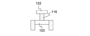
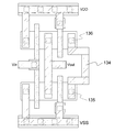
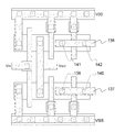
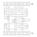
図1、図2、図3及び図4は、本発明の第1の実施形態を示す標準セルのレイアウト構造の簡略図である。
図10は本発明の第2の実施形態を示す標準セルのレイアウト構造の簡略図である。
図11、図12及び図13は、本発明の第3の実施形態を示す標準セルのレイアウト構造の簡略図である。
図15は、本発明の第4の実施形態を示す標準セルのレイアウト構造の簡略図である。
図17は、本発明の第5の実施形態を示す標準セルのレイアウト構造の簡略図である。
(第6の実施形態)
図27は、本発明の第6の実施形態を示す標準セルのレイアウト構造の簡略図である。
図32は、本発明の第7の実施形態を示す標準セルのレイアウト構造の簡略図である。
107〜109 活性ゲート領域
110〜115 ビアコンタクト
116、117 ダミービアコンタクト
118〜121 メタル配線
122、123 ダミーメタル配線
124、126 Nチャネルトランジスタ
125、127 Pチャネルトランジスタ
128、129 不純物拡散領域
130〜133 不純物拡散領域
134 ダミーメタル配線
135、136 ダミービアコンタクト
137、138 ダミーメタル配線
139〜142 ダミービアコンタクト
201、202 不純物拡散領域
203、204 ダミー不純物拡散領域
205、206 ダミーメタル配線
207、208 ダミービアコンタクト
301、302 不純物拡散領域
303 活性ゲート領域
304〜306 ビアコンタクト
307〜309 メタル配線
310 ダミーメタル配線
311 ダミービアコンタクト
401、402 ダミーゲート
403、404 ダミーメタル配線
405、406 ダミービアコンタクト
501〜504 不純物拡散領域
505〜507 活性ゲート領域
508、509 ビアコンタクト
510、511 メタル配線
512 ダミービアコンタクト
513 ダミーメタル配線
514〜516 Nチャネルトランジスタ
517〜519 Pチャネルトランジスタ
520 ダミービアコンタクト
Claims (10)
- オフトランジスタを有する標準セルのレイアウト構造において、
前記オフトランジスタを構成している不純物拡散領域のうち少なくとも1つの領域上にダミービアコンタクトを有する
ことを特徴とする標準セルのレイアウト構造。 - トランジスタを有する標準セルのレイアウト構造において、
前記トランジスタのうち少なくとも1つのトランジスタのゲート上にダミービアコンタクトを有する
ことを特徴とする標準セルのレイアウト構造。 - 前記請求項1記載の標準セルのレイアウト構造において、
前記オフトランジスタを構成している不純物拡散領域の少なくとも1つと、前記オフトランジスタに隣接するトランジスタの不純物拡散領域とが共有されている
ことを特徴とする標準セルのレイアウト構造。 - 前記請求項1記載の標準セルのレイアウト構造において、
前記オフトランジスタが並ぶ本数が複数本である
ことを特徴とする標準セルのレイアウト構造。 - 前記請求項1記載の標準セルのレイアウト構造において、
前記ダミービアコンタクトを複数備え、前記複数のダミービアコンタクト同士がダミーメタル配線で接続されている
ことを特徴とする標準セルのレイアウト構造。 - 前記請求項2記載の標準セルのレイアウト構造において、
前記トランジスタのうちゲート上にダミービアコンタクトを有するトランジスタが、容量トランジスタである
ことを特徴とする標準セルのレイアウト構造。 - 前記請求項2記載の標準セルのレイアウト構造において、
前記トランジスタのうちゲート上にダミービアコンタクトを有するトランジスタのゲート長は、最小のゲート長より大きい
ことを特徴とする標準セルのレイアウト構造。 - 前記請求項1〜7の何れか1項に記載の標準セルのレイアウト構造において、
前記ダミービアコンタクトは、ダミーメタル配線に接続されている
ことを特徴とする標準セルのレイアウト構造。 - 前記請求項1〜8の何れか1項に記載のレイアウト構造を持った標準セルにより構成される
ことを特徴とする標準セルライブラリ。 - LSI上に、前記請求項1〜8の何れか1項に記載のレイアウト構造を持った標準セルが混載されている
ことを特徴とする半導体集積回路のレイアウト構造。
Priority Applications (4)
| Application Number | Priority Date | Filing Date | Title |
|---|---|---|---|
| JP2008115188A JP5230251B2 (ja) | 2008-04-25 | 2008-04-25 | 標準セルのレイアウト構造、標準セルライブラリ、及び半導体集積回路のレイアウト構造 |
| PCT/JP2009/001188 WO2009130844A1 (ja) | 2008-04-25 | 2009-03-17 | 標準セルのレイアウト構造、標準セルライブラリ、及び半導体集積回路のレイアウト構造 |
| US12/905,873 US8766322B2 (en) | 2008-04-25 | 2010-10-15 | Layout structure of standard cell, standard cell library, and layout structure of semiconductor integrated circuit |
| US14/281,662 US9147652B2 (en) | 2008-04-25 | 2014-05-19 | Layout structure of standard cell, standard cell library, and layout structure of semiconductor integrated circuit |
Applications Claiming Priority (1)
| Application Number | Priority Date | Filing Date | Title |
|---|---|---|---|
| JP2008115188A JP5230251B2 (ja) | 2008-04-25 | 2008-04-25 | 標準セルのレイアウト構造、標準セルライブラリ、及び半導体集積回路のレイアウト構造 |
Publications (2)
| Publication Number | Publication Date |
|---|---|
| JP2009267094A JP2009267094A (ja) | 2009-11-12 |
| JP5230251B2 true JP5230251B2 (ja) | 2013-07-10 |
Family
ID=41216587
Family Applications (1)
| Application Number | Title | Priority Date | Filing Date |
|---|---|---|---|
| JP2008115188A Active JP5230251B2 (ja) | 2008-04-25 | 2008-04-25 | 標準セルのレイアウト構造、標準セルライブラリ、及び半導体集積回路のレイアウト構造 |
Country Status (3)
| Country | Link |
|---|---|
| US (2) | US8766322B2 (ja) |
| JP (1) | JP5230251B2 (ja) |
| WO (1) | WO2009130844A1 (ja) |
Cited By (1)
| Publication number | Priority date | Publication date | Assignee | Title |
|---|---|---|---|---|
| KR101429396B1 (ko) | 2013-01-28 | 2014-08-11 | 타이완 세미콘덕터 매뉴팩쳐링 컴퍼니 리미티드 | 표준 셀 디자인 레이아웃 |
Families Citing this family (30)
| Publication number | Priority date | Publication date | Assignee | Title |
|---|---|---|---|---|
| US8004014B2 (en) * | 2008-07-04 | 2011-08-23 | Panasonic Corporation | Semiconductor integrated circuit device having metal interconnect regions placed symmetrically with respect to a cell boundary |
| JP5594294B2 (ja) | 2009-12-25 | 2014-09-24 | パナソニック株式会社 | 半導体装置 |
| WO2012070821A2 (ko) * | 2010-11-22 | 2012-05-31 | 한양대학교 산학협력단 | 플립플롭 회로의 레이아웃 라이브러리 |
| US8957480B2 (en) | 2011-03-04 | 2015-02-17 | Renesas Electronics Corporation | Semiconductor device including dummy transistors with reduced off-leakage current |
| US8836040B2 (en) * | 2012-11-07 | 2014-09-16 | Qualcomm Incorporated | Shared-diffusion standard cell architecture |
| US9024418B2 (en) * | 2013-03-14 | 2015-05-05 | Qualcomm Incorporated | Local interconnect structures for high density |
| US8759885B1 (en) | 2013-04-30 | 2014-06-24 | Freescale Semiconductor, Inc. | Standard cell for semiconductor device |
| CN105531813B (zh) * | 2013-09-04 | 2018-10-12 | 株式会社索思未来 | 半导体装置 |
| KR102046986B1 (ko) | 2013-09-27 | 2019-11-20 | 삼성전자 주식회사 | 더미 셀 어레이를 포함하는 반도체 소자 |
| FR3018139B1 (fr) | 2014-02-28 | 2018-04-27 | Stmicroelectronics (Rousset) Sas | Circuit integre a composants, par exemple transistors nmos, a regions actives a contraintes en compression relachees |
| US9318476B2 (en) * | 2014-03-03 | 2016-04-19 | Qualcomm Incorporated | High performance standard cell with continuous oxide definition and characterized leakage current |
| US9852252B2 (en) | 2014-08-22 | 2017-12-26 | Samsung Electronics Co., Ltd. | Standard cell library and methods of using the same |
| FR3025335B1 (fr) * | 2014-08-29 | 2016-09-23 | Stmicroelectronics Rousset | Procede de fabrication d'un circuit integre rendant plus difficile une retro-conception du circuit integre et circuit integre correspondant |
| KR102173638B1 (ko) | 2014-10-01 | 2020-11-04 | 삼성전자주식회사 | 반도체 소자 및 그 형성방법 |
| KR102358571B1 (ko) | 2015-07-29 | 2022-02-07 | 삼성전자주식회사 | 집적 회로 및 표준 셀 라이브러리 |
| KR102314778B1 (ko) | 2015-08-21 | 2021-10-21 | 삼성전자주식회사 | 반도체 소자 |
| KR102382826B1 (ko) | 2015-09-08 | 2022-04-04 | 삼성전자주식회사 | 반도체 장치의 제조 방법 |
| KR102521554B1 (ko) | 2015-12-07 | 2023-04-13 | 삼성전자주식회사 | 배선 구조물, 배선 구조물 설계 방법, 및 배선 구조물 형성 방법 |
| CN107706233B (zh) * | 2016-08-08 | 2022-07-12 | 联华电子股份有限公司 | 半导体元件及其制作方法 |
| US10339250B2 (en) * | 2016-11-29 | 2019-07-02 | Taiwan Semiconductor Manufacturing Company, Ltd. | Method of generating engineering change order (ECO) layout of base cell and computer-readable medium comprising executable instructions for carrying out said method |
| KR102308779B1 (ko) | 2017-04-10 | 2021-10-05 | 삼성전자주식회사 | 이종 컨택들을 구비하는 집적 회로 및 이를 포함하는 반도체 장치 |
| US10332870B2 (en) | 2017-06-01 | 2019-06-25 | Samsung Electronics Co, Ltd. | Semiconductor device including a field effect transistor |
| KR102379450B1 (ko) | 2017-06-01 | 2022-03-30 | 삼성전자주식회사 | 반도체 소자 |
| US10692808B2 (en) | 2017-09-18 | 2020-06-23 | Qualcomm Incorporated | High performance cell design in a technology with high density metal routing |
| US10665591B2 (en) * | 2018-09-05 | 2020-05-26 | Arm Limited | Transistor gate arrangement to modify driver signal characteristics |
| CN113196464B (zh) * | 2018-12-25 | 2024-05-28 | 株式会社索思未来 | 半导体集成电路装置 |
| KR102868418B1 (ko) * | 2019-11-29 | 2025-10-13 | 삼성전자주식회사 | 집적된 표준셀 구조를 포함하는 집적 회로 |
| US11133272B1 (en) * | 2020-04-23 | 2021-09-28 | Qualcomm Incorporated | Vertically-aligned and conductive dummies in integrated circuit layers for capacitance reduction and bias independence and methods of manufacture |
| US11574901B2 (en) | 2020-04-29 | 2023-02-07 | Taiwan Semiconductor Manufacturing Company, Ltd. | Semiconductor device and method for manufacturing the same |
| TWI751065B (zh) | 2020-04-29 | 2021-12-21 | 台灣積體電路製造股份有限公司 | 半導體元件及其製造方法 |
Family Cites Families (16)
| Publication number | Priority date | Publication date | Assignee | Title |
|---|---|---|---|---|
| US5304835A (en) * | 1990-07-18 | 1994-04-19 | Seiko Epson Corporation | Semiconductor device |
| JPH04105359A (ja) * | 1990-08-23 | 1992-04-07 | Sony Corp | 大ゲート面積mosトランジスタ |
| JPH0685080A (ja) | 1992-08-31 | 1994-03-25 | Nippon Steel Corp | 半導体装置及びその製造方法 |
| JPH07273300A (ja) | 1994-03-29 | 1995-10-20 | Sony Corp | Cmos否定論理回路構造およびそのレイアウト配線方法 |
| DE10008243B4 (de) * | 2000-02-23 | 2005-09-22 | Infineon Technologies Ag | Integrierter Speicher mit Plattenleitungssegmenten |
| JP4090222B2 (ja) | 2001-07-17 | 2008-05-28 | 株式会社ルネサステクノロジ | 半導体集積回路、該半導体集積回路の設計方法及び該半導体集積回路設計用プログラム |
| US6854139B2 (en) | 2002-07-26 | 2005-02-15 | Sheila Lamy | Bed covering fastening system |
| JP2005268610A (ja) * | 2004-03-19 | 2005-09-29 | Matsushita Electric Ind Co Ltd | スタンダードセルの設計方法及び半導体集積回路 |
| JP2006100307A (ja) * | 2004-09-28 | 2006-04-13 | Renesas Technology Corp | ダミー配線を配置した半導体装置とダミーパターンの作成方法 |
| JP4998970B2 (ja) * | 2005-01-26 | 2012-08-15 | ルネサスエレクトロニクス株式会社 | スタティック半導体記憶装置 |
| JP2007129030A (ja) | 2005-11-02 | 2007-05-24 | Seiko Epson Corp | 半導体装置及びその製造方法 |
| US7343570B2 (en) | 2005-11-02 | 2008-03-11 | International Business Machines Corporation | Methods, systems, and media to improve manufacturability of semiconductor devices |
| JP2007250705A (ja) | 2006-03-15 | 2007-09-27 | Nec Electronics Corp | 半導体集積回路装置及びダミーパターンの配置方法 |
| JP2007305713A (ja) | 2006-05-10 | 2007-11-22 | Matsushita Electric Ind Co Ltd | 半導体装置及び配線補助パターン生成方法 |
| JP4973224B2 (ja) * | 2006-07-19 | 2012-07-11 | 富士通セミコンダクター株式会社 | 電子回路装置設計方法、電子ビーム露光データ作成方法、及び、電子ビーム露光方法 |
| JP4809319B2 (ja) * | 2007-11-22 | 2011-11-09 | パナソニック株式会社 | 半導体装置および半導体マスクレイアウト方法 |
-
2008
- 2008-04-25 JP JP2008115188A patent/JP5230251B2/ja active Active
-
2009
- 2009-03-17 WO PCT/JP2009/001188 patent/WO2009130844A1/ja not_active Ceased
-
2010
- 2010-10-15 US US12/905,873 patent/US8766322B2/en active Active
-
2014
- 2014-05-19 US US14/281,662 patent/US9147652B2/en active Active
Cited By (3)
| Publication number | Priority date | Publication date | Assignee | Title |
|---|---|---|---|---|
| KR101429396B1 (ko) | 2013-01-28 | 2014-08-11 | 타이완 세미콘덕터 매뉴팩쳐링 컴퍼니 리미티드 | 표준 셀 디자인 레이아웃 |
| US8813016B1 (en) | 2013-01-28 | 2014-08-19 | Taiwan Semiconductor Manufacturing Company Limited | Multiple via connections using connectivity rings |
| US9213795B2 (en) | 2013-01-28 | 2015-12-15 | Taiwan Semiconductor Manufacturing Company Limited | Multiple via connections using connectivity rings |
Also Published As
| Publication number | Publication date |
|---|---|
| JP2009267094A (ja) | 2009-11-12 |
| US20140252653A1 (en) | 2014-09-11 |
| WO2009130844A1 (ja) | 2009-10-29 |
| US9147652B2 (en) | 2015-09-29 |
| US20110031536A1 (en) | 2011-02-10 |
| US8766322B2 (en) | 2014-07-01 |
Similar Documents
| Publication | Publication Date | Title |
|---|---|---|
| JP5230251B2 (ja) | 標準セルのレイアウト構造、標準セルライブラリ、及び半導体集積回路のレイアウト構造 | |
| US10692856B2 (en) | Semiconductor integrated circuit device | |
| US7737472B2 (en) | Semiconductor integrated circuit device | |
| US8174052B2 (en) | Standard cell libraries and integrated circuit including standard cells | |
| US7772070B2 (en) | Semiconductor integrated circuit device and dummy pattern arrangement method | |
| JP4841204B2 (ja) | 半導体装置 | |
| EP1315210A1 (en) | Multi-threshold mis integrated circuit device and circuit design method thereof | |
| JP5896682B2 (ja) | 半導体集積回路装置 | |
| JP2008192841A (ja) | 半導体集積回路 | |
| US9373611B2 (en) | Semiconductor integrated circuit device | |
| JP2008118004A (ja) | 半導体集積回路 | |
| JP2013120852A (ja) | スタンダードセル、および、半導体集積回路 | |
| JP2011060942A (ja) | 半導体装置、半導体装置の製造方法、及び半導体装置のレイアウト方法 | |
| CN112567507A (zh) | 半导体集成电路装置 | |
| US7868359B2 (en) | Semiconductor device | |
| JP5653001B2 (ja) | 半導体装置及び半導体装置の補償容量の配置方法 | |
| JP2008258424A (ja) | 半導体集積回路装置 | |
| CN118318295A (zh) | 半导体集成电路装置 | |
| JP3891813B2 (ja) | 集積論理回路の階層設計方法 | |
| JP5956964B2 (ja) | 半導体装置 | |
| US7968917B2 (en) | Semiconductor memory device | |
| JP2016066823A (ja) | 半導体集積回路装置 | |
| JP2014103346A (ja) | 半導体装置 | |
| JP2005353683A (ja) | 半導体集積回路 |
Legal Events
| Date | Code | Title | Description |
|---|---|---|---|
| A621 | Written request for application examination |
Free format text: JAPANESE INTERMEDIATE CODE: A621 Effective date: 20110331 |
|
| RD02 | Notification of acceptance of power of attorney |
Free format text: JAPANESE INTERMEDIATE CODE: A7422 Effective date: 20120131 |
|
| A131 | Notification of reasons for refusal |
Free format text: JAPANESE INTERMEDIATE CODE: A131 Effective date: 20121211 |
|
| A521 | Request for written amendment filed |
Free format text: JAPANESE INTERMEDIATE CODE: A523 Effective date: 20130201 |
|
| TRDD | Decision of grant or rejection written | ||
| A01 | Written decision to grant a patent or to grant a registration (utility model) |
Free format text: JAPANESE INTERMEDIATE CODE: A01 Effective date: 20130219 |
|
| A61 | First payment of annual fees (during grant procedure) |
Free format text: JAPANESE INTERMEDIATE CODE: A61 Effective date: 20130319 |
|
| FPAY | Renewal fee payment (event date is renewal date of database) |
Free format text: PAYMENT UNTIL: 20160329 Year of fee payment: 3 |
|
| R150 | Certificate of patent or registration of utility model |
Ref document number: 5230251 Country of ref document: JP Free format text: JAPANESE INTERMEDIATE CODE: R150 Free format text: JAPANESE INTERMEDIATE CODE: R150 |
|
| S111 | Request for change of ownership or part of ownership |
Free format text: JAPANESE INTERMEDIATE CODE: R313111 |
|
| R350 | Written notification of registration of transfer |
Free format text: JAPANESE INTERMEDIATE CODE: R350 |
|
| R250 | Receipt of annual fees |
Free format text: JAPANESE INTERMEDIATE CODE: R250 |