JP5241477B2 - Wiring board and wiring module - Google Patents

Wiring board and wiring module Download PDF

Info

Publication number
JP5241477B2
JP5241477B2 JP2008329526A JP2008329526A JP5241477B2 JP 5241477 B2 JP5241477 B2 JP 5241477B2 JP 2008329526 A JP2008329526 A JP 2008329526A JP 2008329526 A JP2008329526 A JP 2008329526A JP 5241477 B2 JP5241477 B2 JP 5241477B2
Authority
JP
Japan
Prior art keywords
signal line
wiring
wiring board
signal
conductors
Prior art date
Legal status (The legal status is an assumption and is not a legal conclusion. Google has not performed a legal analysis and makes no representation as to the accuracy of the status listed.)
Active
Application number
JP2008329526A
Other languages
Japanese (ja)
Other versions
JP2010153557A (en
Inventor
隆行 白崎
Current Assignee (The listed assignees may be inaccurate. Google has not performed a legal analysis and makes no representation or warranty as to the accuracy of the list.)
Kyocera Corp
Original Assignee
Kyocera Corp
Priority date (The priority date is an assumption and is not a legal conclusion. Google has not performed a legal analysis and makes no representation as to the accuracy of the date listed.)
Filing date
Publication date
Application filed by Kyocera Corp filed Critical Kyocera Corp
Priority to JP2008329526A priority Critical patent/JP5241477B2/en
Publication of JP2010153557A publication Critical patent/JP2010153557A/en
Application granted granted Critical
Publication of JP5241477B2 publication Critical patent/JP5241477B2/en
Active legal-status Critical Current
Anticipated expiration legal-status Critical

Links

Images

Landscapes

  • Structure Of Printed Boards (AREA)

Description

本発明は、配線基板のうち高周波用配線基板に関するものである。高周波用配線基板は、例えば、光通信、無線通信のような高周波通信の分野で好適に用いることができる。   The present invention relates to a high-frequency wiring board among wiring boards. The high frequency wiring board can be suitably used in the field of high frequency communication such as optical communication and wireless communication.

従来から、高周波通信の分野で用いられる配線基板には、半導体素子などの電子部品から信号の入出力を行う電気配線が複数備えられている。そして、これらの電気配線における高周波信号の伝播時間のばらつきを小さくすることが求められている。そこで、特許文献1に開示されているように、各電気配線の途中に湾曲部を設けた配線基板が提案されている。   Conventionally, a wiring board used in the field of high-frequency communication has been provided with a plurality of electric wirings for inputting and outputting signals from electronic components such as semiconductor elements. And it is calculated | required to reduce the dispersion | variation in the propagation time of the high frequency signal in these electric wiring. Therefore, as disclosed in Patent Document 1, a wiring board in which a curved portion is provided in the middle of each electric wiring has been proposed.

特許文献1に開示された配線基板においては、各電気配線の途中に湾曲部を設けて、各電気配線の長さを実質的に等しくすることにより、高周波信号の伝播時間のばらつきを小さくしている。また、特許文献1には、互いに異なる比誘電率を有する電気絶縁層を重ねることにより、各電気配線における伝播時間のばらつきを小さくした配線基板も開示されている。
特開平11−8444号公報
In the wiring board disclosed in Patent Document 1, a curved portion is provided in the middle of each electrical wiring, and the length of each electrical wiring is made substantially equal, thereby reducing variations in the propagation time of high-frequency signals. Yes. Patent Document 1 also discloses a wiring board in which variation in propagation time in each electric wiring is reduced by overlapping electric insulating layers having different relative dielectric constants.
Japanese Patent Laid-Open No. 11-8444

しかしながら、各電気配線の途中に湾曲部を設けて、各電気配線の長さを実質的に等しくする場合、湾曲部を設ける領域が必要なため、配線基板の小型化が困難となる場合がある。また、互いに異なる比誘電率を有する電気絶縁層を積層した配線基板を用いた場合、各電気配線の長さに応じた比誘電率を有する電気絶縁層を積層する必要がある。そのため、製造コストが増大する可能性があった。   However, when a curved portion is provided in the middle of each electrical wiring and the length of each electrical wiring is made substantially equal, a region for providing the curved portion is required, and thus it may be difficult to reduce the size of the wiring board. . In addition, when a wiring board in which electrical insulating layers having different relative dielectric constants are stacked is used, it is necessary to stack electrical insulating layers having a relative dielectric constant corresponding to the length of each electrical wiring. Therefore, the manufacturing cost may increase.

本発明は、上記課題に鑑みてなされたものであり、小型化が容易であるとともに高周波信号の伝播時間のばらつきを容易に抑制することのできる配線基板を提供することを目的とする。   The present invention has been made in view of the above problems, and an object of the present invention is to provide a wiring board that can be easily miniaturized and can easily suppress variations in the propagation time of high-frequency signals.

本発明の配線基板は、主面を有する誘電体基板と、該誘電体基板の主面上に配設された第1の信号線路と、前記誘電体基板の主面上に配設され、前記第1の信号線路よりも短い第2の信号線路と、前記第1の信号線路に沿って併設されるとともに基準電位に接続された第1の基準導体と、前記第2の信号線路に沿って併設されるとともに基準電位に接続され、前記第2の信号線路の配線方向に離隔する複数の第2の基準導体とを備えている。   The wiring board of the present invention is provided on the main surface of the dielectric substrate having a main surface of the dielectric substrate, a first signal line disposed on the main surface of the dielectric substrate, A second signal line shorter than the first signal line, a first reference conductor provided along the first signal line and connected to a reference potential, and along the second signal line And a plurality of second reference conductors that are connected to a reference potential and spaced apart in the wiring direction of the second signal line.

本発明の配線基板によれば、第2の信号線路に沿って併設されるとともに基準電位に接続され、第2の信号線路の配線方向に離隔する複数の第2の基準導体を備えている。第2の信号線路において、第2の基準導体に併設された部分と複数の第2の基準導体間に位置する部分とでは信号の伝播モードが変化する。そのため、複数の第2の基準導体間に位置する部分における信号の伝達速度が第2の基準導体に併設された部分における信号の伝達速度よりも低下する。これにより、相対的に配線距離の短い第2の信号線路における信号の伝播時間を相対的に配線距離の長い第1の信号線路における信号の伝播時間に近づけることができる。結果として、第1の信号線路と第2の信号線路との間で生じる伝播時間のばらつきを容易に抑制することが可能となる。   According to the wiring board of the present invention, a plurality of second reference conductors are provided along the second signal line, connected to the reference potential, and spaced apart in the wiring direction of the second signal line. In the second signal line, the signal propagation mode changes between a portion provided adjacent to the second reference conductor and a portion positioned between the plurality of second reference conductors. For this reason, the signal transmission speed in the portion located between the plurality of second reference conductors is lower than the signal transmission speed in the portion adjacent to the second reference conductor. Thereby, the signal propagation time in the second signal line having a relatively short wiring distance can be made closer to the signal propagation time in the first signal line having a relatively long wiring distance. As a result, it is possible to easily suppress variations in propagation time that occur between the first signal line and the second signal line.

以下、本発明の配線基板について図面を用いて詳細に説明する。   Hereinafter, the wiring board of the present invention will be described in detail with reference to the drawings.

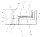
図1〜4に示すように、本発明の第1の実施形態にかかる配線基板1は、主面を有する誘電体基板3と、誘電体基板3の主面上に配設された第1の信号線路5と、誘電体基板3の主面上に配設され、第1の信号線路5よりも短い第2の信号線路7と、第1の信号線路5に沿って併設されるとともに基準電位に接続される第1の基準導体9と、第2の信号線路7に沿って併設されるとともに基準電位に接続され、第2の信号線路7の配線方向に離隔する複数の第2の基準導体11とを備えている。   As shown in FIGS. 1 to 4, the wiring substrate 1 according to the first embodiment of the present invention includes a dielectric substrate 3 having a main surface, and a first substrate disposed on the main surface of the dielectric substrate 3. The signal line 5 is disposed on the main surface of the dielectric substrate 3, and is provided along the first signal line 5, the second signal line 7 shorter than the first signal line 5, and the reference potential And a plurality of second reference conductors that are provided along the second signal line 7 and connected to the reference potential and spaced apart in the wiring direction of the second signal line 7 11.

このように、本実施形態にかかる配線基板1は、第2の信号線路7に沿って併設されるとともに基準電位に接続され、第2の信号線路7の配線方向に離隔する複数の第2の基準導体11を備えている。そのため、相対的に配線距離の短い第2の信号線路7における信号の伝播時間を相対的に配線距離の長い第1の信号線路5における信号の伝播時間に近づけることができる。結果として、第1の信号線路5と第2の信号線路7との間で生じる伝播時間のばらつきを容易に抑制することが可能となる。   As described above, the wiring board 1 according to the present embodiment is provided along the second signal line 7 and connected to the reference potential, and is separated from each other in the wiring direction of the second signal line 7. A reference conductor 11 is provided. Therefore, the signal propagation time in the second signal line 7 having a relatively short wiring distance can be made closer to the signal propagation time in the first signal line 5 having a relatively long wiring distance. As a result, it is possible to easily suppress variations in propagation time that occur between the first signal line 5 and the second signal line 7.

本実施形態にかかる配線基板1は、主面を有する誘電体基板3を備えている。誘電体基板3としては、絶縁性の部材を用いることができる。具体的には、酸化アルミニウム,窒化アルミニウム,窒化珪素,ムライト等を主成分とするセラミック材料,ガラス,あるいはガラスとセラミックフィラーとの混合物を焼成して形成されたガラスセラミック材料,エポキシ樹脂,ポリイミド樹脂,四フッ化エチレン樹脂を始めとするフッ素系樹脂等の有機樹脂系材料,有機樹脂−セラミック(ガラスも含む)複合系材料等が用いることができる。   The wiring board 1 according to the present embodiment includes a dielectric substrate 3 having a main surface. As the dielectric substrate 3, an insulating member can be used. Specifically, ceramic materials mainly composed of aluminum oxide, aluminum nitride, silicon nitride, mullite, etc., glass ceramic materials formed by firing glass or a mixture of glass and ceramic filler, epoxy resin, polyimide resin Organic resin materials such as fluororesins such as tetrafluoroethylene resin, organic resin-ceramic (including glass) composite materials, and the like can be used.

特に、誘電体基板3としてはセラミックス材料を用いることが好ましい。これは、セラミック材料は低損失材料であることから、高周波信号を損失なく伝送することができるからである。また、熱伝導率が高く、温度による物性変化が小さいため、抵抗体などで発生した熱による特性変動を抑えることができる。   In particular, it is preferable to use a ceramic material for the dielectric substrate 3. This is because the ceramic material is a low-loss material and can transmit a high-frequency signal without loss. In addition, since the thermal conductivity is high and the change in physical properties due to temperature is small, it is possible to suppress fluctuations in characteristics due to heat generated in a resistor or the like.

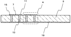
また、本実施形態における誘電体基板3は、主面から裏面にかけて貫通する貫通孔を複数有している。また、これらの貫通孔にはそれぞれビア導体13が配設されている。ビア導体13は、誘電体基板3の主面上において第1の基準導体9又は第2の基準導体11の何れかと電気的に接続されている。   Further, the dielectric substrate 3 in the present embodiment has a plurality of through holes penetrating from the main surface to the back surface. In addition, via conductors 13 are disposed in these through holes, respectively. The via conductor 13 is electrically connected to either the first reference conductor 9 or the second reference conductor 11 on the main surface of the dielectric substrate 3.

本実施形態にかかる配線基板1は、誘電体基板3の主面上に配設された第1の信号線路5及び第2の信号線路7を備えている。このとき、第2の信号線路7は第1の信号線路5よりも短くなるように配設されている。これらの信号線路は、配線基板1の主面上に配設される電子部品23に信号を入力又は出力するための配線として用いられている。   The wiring board 1 according to the present embodiment includes a first signal line 5 and a second signal line 7 disposed on the main surface of the dielectric substrate 3. At this time, the second signal line 7 is arranged to be shorter than the first signal line 5. These signal lines are used as wirings for inputting or outputting signals to the electronic component 23 disposed on the main surface of the wiring board 1.

また、第1の信号線路5及び第2の信号線路7は、外部に対して電気的な接続を容易に行うため、電子部品が電気的に接続されるところの一方端における第1の信号線路5と第2の信号線路7との間隔よりも、外部配線と接続されるところの他方端における第1の信号線路5と第2の信号線路7との間隔が広くなっている。第1の信号線路5及び第2の信号線路7の一方端と電子部品とを電気的に接続することにより、小型の電子部品に対しても外部配線の接続を容易に行うことができる。   The first signal line 5 and the second signal line 7 are easily connected to the outside, so that the first signal line at one end where the electronic component is electrically connected is provided. The distance between the first signal line 5 and the second signal line 7 at the other end connected to the external wiring is wider than the distance between the second signal line 7 and the second signal line 7. By electrically connecting one end of the first signal line 5 and the second signal line 7 and the electronic component, external wiring can be easily connected to a small electronic component.

一方、このように小型の電子部品に対して外部配線の接続を容易に行うため、一方端における第1の信号線路5と第2の信号線路7の間隔よりも一方端における第1の信号線路5と第2の信号線路7の間隔を広くすることから、第1の信号線路5と第2の信号線路7の長さを変えることが必要となる。しかしながら、第1の信号線路5と第2の信号線路7の長さを変えた場合、信号の伝播時間に時間差が生じる。特に、第1の信号線路5及び第2の信号線路7だけでなく、信号線路を多数配設した場合、これらの信号線路における伝播時間にばらつきが生じる可能性がある。本実施形態にかかる配線基板1においては、後述するように、互いに離隔する複数の第2の基準導体11を備えていることにより、上記の伝播時間のずれを小さくすることができる。   On the other hand, in order to easily connect external wiring to such a small electronic component, the first signal line at one end rather than the distance between the first signal line 5 and the second signal line 7 at one end. Therefore, it is necessary to change the lengths of the first signal line 5 and the second signal line 7. However, when the lengths of the first signal line 5 and the second signal line 7 are changed, a time difference occurs in the signal propagation time. In particular, when not only the first signal line 5 and the second signal line 7 but also a large number of signal lines are provided, there is a possibility that the propagation time in these signal lines varies. As will be described later, the wiring board 1 according to the present embodiment includes a plurality of second reference conductors 11 that are spaced apart from each other, thereby reducing the above-described shift in propagation time.

第1の信号線路5及び第2の信号線路7としては、電気伝導性の良好な部材を用いることが好ましく、例えば、Au,Ag,Cu,Al,Pt,Pd,W及びMoのような金属部材を用いることができる。   As the first signal line 5 and the second signal line 7, it is preferable to use a member having good electrical conductivity. For example, a metal such as Au, Ag, Cu, Al, Pt, Pd, W, and Mo is used. A member can be used.

本実施形態にかかる配線基板1は、第1の信号線路5に沿って併設されるとともに基準電位に接続された第1の基準導体9を備えている。このような第1の基準導体9を備えていることにより、複数の信号線路間における短絡、及び第1の信号線路5と第1の基準導体9との間での共振が生じる可能性を低減することができる。そのため、安定して信号を伝播することが可能となる。   The wiring board 1 according to the present embodiment includes a first reference conductor 9 that is provided along the first signal line 5 and connected to a reference potential. By including the first reference conductor 9 as described above, it is possible to reduce the possibility of short circuit between a plurality of signal lines and resonance between the first signal line 5 and the first reference conductor 9. can do. Therefore, it becomes possible to propagate the signal stably.

第1の基準導体9としては、第1の信号線路5と同様に電気伝導性の良好な部材を用いることが好ましい。具体的には、Au,Ag,Cu,Al,Pt,Pd,W及びMoのような金属部材を用いることができる。   As the first reference conductor 9, it is preferable to use a member having good electrical conductivity as in the first signal line 5. Specifically, metal members such as Au, Ag, Cu, Al, Pt, Pd, W, and Mo can be used.

本実施形態にかかる配線基板1は、第2の信号線路7に沿って併設されるとともに基準電位に接続された複数の第2の基準導体11を備えている。このような第2の基準導体11を備えていることにより、第1の基準導体9と同様に、複数の信号線路間における短絡、及び第2の信号線路7と第2の基準導体11との間での共振が生じる可能性を低減することができる。   The wiring board 1 according to the present embodiment includes a plurality of second reference conductors 11 provided along the second signal line 7 and connected to a reference potential. By providing such a second reference conductor 11, similarly to the first reference conductor 9, a short circuit between a plurality of signal lines, and a relationship between the second signal line 7 and the second reference conductor 11. It is possible to reduce the possibility of resonance between the two.

そして、本実施形態にかかる複数の第2の基準導体11は、第2の信号線路7の配線方向に離隔するように配設されている。言い換えれば、第2の信号線路7が、第2の基準導体11が併設された部分(以下、第1の部位7aともいう)と、それ以外の第2の基準導体11が併設されていない部分(以下、第2の部位7bともいう)とを有している。   The plurality of second reference conductors 11 according to the present embodiment are disposed so as to be separated in the wiring direction of the second signal line 7. In other words, the second signal line 7 includes a portion where the second reference conductor 11 is provided (hereinafter also referred to as the first portion 7a) and a portion where the other second reference conductor 11 is not provided. (Hereinafter also referred to as second portion 7b).

このように、第2の信号線路7が第1の部位7a及び第2の部位7bを有している場合、第1の部位7aと第2の部位7bとでは電気信号の伝播モードが変化するため、第2の部位7bにおける信号の伝播速度が第1の部位7aにおける信号の伝播速度よりも遅くなる。これにより、相対的に配線距離の短い第2の信号線路7における信号の伝播時間を相対的に配線距離の長い第1の信号線路5における信号の伝播時間に近づけることができる。なお、互いに離隔するように配設された複数の第2の基準導体11間の間隔は、第1の信号線路5と第2の信号線路7の長さの差に応じて設定すればよい。   As described above, when the second signal line 7 has the first part 7a and the second part 7b, the propagation mode of the electric signal changes between the first part 7a and the second part 7b. Therefore, the propagation speed of the signal in the second part 7b is slower than the propagation speed of the signal in the first part 7a. Thereby, the signal propagation time in the second signal line 7 having a relatively short wiring distance can be made closer to the signal propagation time in the first signal line 5 having a relatively long wiring distance. In addition, what is necessary is just to set the space | interval between the several 2nd reference conductors 11 arrange | positioned mutually spaced apart according to the difference of the length of the 1st signal track | line 5 and the 2nd signal track | line 7.

また、第2の基準導体11の幅は、第1の信号線路5及び第2の信号線路7において伝播される信号の波長の1/2より小さいことが好ましい。若しくは、複数の第2の基準導体11間の間隔が、併設された信号線路側とその反対側ではテーパーや階段形状により異なっていることが好ましい。これにより、互いに離隔するように配設された複数の第2の基準導体11間の間隔がスタブ線路として働き、共振などが生じる可能性を低減することができる。   Further, the width of the second reference conductor 11 is preferably smaller than ½ of the wavelength of the signal propagated in the first signal line 5 and the second signal line 7. Alternatively, the interval between the plurality of second reference conductors 11 is preferably different depending on the taper or the step shape on the side of the signal line provided on the side and the opposite side. Thereby, the space | interval between the some 2nd reference conductors 11 arrange | positioned so that it may mutually space apart can work | function as a stub line, and can reduce possibility that resonance etc. will arise.

第2の基準導体11としては、第1の信号線路5と同様に電気伝導性の良好な部材を用いることが好ましい。具体的には、Au,Ag,Cu,Al,Pt,Pd,W及びMoのような金属部材を用いることができる。   As the second reference conductor 11, it is preferable to use a member having good electrical conductivity like the first signal line 5. Specifically, metal members such as Au, Ag, Cu, Al, Pt, Pd, W, and Mo can be used.

また、本実施形態にかかる配線基板1は、第1の基準導体9とは反対側で第1の信号線路5に沿って併設されるとともに第2の基準導体11とは反対側で第2の信号線路7に沿って併設され、それぞれ基準電位に接続された複数の第3の基準導体15を更に備えている。言い換えれば、第1の信号線路5が第1の基準導体9と第3の基準導体15との間に位置するとともに、第2の信号線路7が第2の基準導体11と第3の基準導体15との間に位置している。   In addition, the wiring board 1 according to the present embodiment is provided along the first signal line 5 on the side opposite to the first reference conductor 9 and the second side on the side opposite to the second reference conductor 11. A plurality of third reference conductors 15 are further provided along the signal line 7 and connected to the reference potential. In other words, the first signal line 5 is located between the first reference conductor 9 and the third reference conductor 15, and the second signal line 7 is the second reference conductor 11 and the third reference conductor. 15 is located between.

本実施形態にかかる配線基板1は、上記のように配設された第3の基準導体15を更に備えていることにより、複数の信号線路間、及び信号線路と基準導体との間での共振が生じる可能性を低減することができるからである。そのため、より安定して信号を伝播することが可能となる。
The wiring board 1 according to the present embodiment further includes the third reference conductor 15 arranged as described above, thereby resonating between a plurality of signal lines and between the signal lines and the reference conductor. This is because the possibility of occurrence of the occurrence can be reduced. Therefore, it becomes possible to propagate the signal more stably.

第2の基準導体11としては、第1の信号線路5と同様に電気伝導性の良好な部材を用いることが好ましい。具体的には、Au,Ag,Cu,Al,Pt,Pd,W及びMoのような金属部材を用いることができる。   As the second reference conductor 11, it is preferable to use a member having good electrical conductivity like the first signal line 5. Specifically, metal members such as Au, Ag, Cu, Al, Pt, Pd, W, and Mo can be used.

また、本実施形態にかかる配線基板1のように、第2の信号線路7が、複数の第2の基準導体11に併設された部分における幅よりも、複数の第2の基準導体11間に位置する部分における幅が大きい形状であることが好ましい。これにより、特性インピーダンスマッチングを良好に行うことができる。そのため、低反射な配線基板1とすることができる。   In addition, as in the wiring board 1 according to the present embodiment, the second signal line 7 is located between the plurality of second reference conductors 11 rather than the width of the portion where the second signal lines 7 are provided side by side with the plurality of second reference conductors 11. It is preferable that it is a shape with a large width | variety in the part located. Thereby, characteristic impedance matching can be performed satisfactorily. Therefore, the wiring board 1 having low reflection can be obtained.

このとき、第2の信号線路7が複数の第2の基準導体11間に位置する部分に第2の基準導体11と対向する一方側に凸部19を有していることがより好ましい。このような凸部19を有することによって複数の第2の基準導体11に併設された部分における幅よりも、複数の第2の基準導体11間に位置する部分における幅が大きい形状である場合には、より高周波帯の信号を良好に伝播することができる。第2の信号線路7の他方側に併設された第3の基準導体15との間隔を一定に保つことができるので、信号の伝播モードの不連続性を抑制することができるからである。   At this time, it is more preferable that the second signal line 7 has a convex portion 19 on one side facing the second reference conductor 11 at a portion located between the plurality of second reference conductors 11. By having such a convex portion 19, the width at the portion located between the plurality of second reference conductors 11 is larger than the width at the portion provided alongside the plurality of second reference conductors 11. Can better propagate signals in a higher frequency band. This is because the distance from the third reference conductor 15 provided on the other side of the second signal line 7 can be kept constant, so that discontinuity of the signal propagation mode can be suppressed.

また、本実施形態にかかる配線基板1のように、第2の信号線路7は、直線部分を有し、直線部分において複数の第2の基準導体11が第2の信号線路7の配線方向に離隔していることが好ましい。第2の信号線路7の曲線部分において複数の第2の基準導体11が互いに離隔している場合と比較して、ノイズの発生を抑制することができるからである。また、第2の信号線路7の曲線部分において複数の第2の基準導体11が互いに離隔している場合と比較して、電磁波の放射による放射損を少なくことができる。   Further, like the wiring board 1 according to the present embodiment, the second signal line 7 has a straight line portion, and a plurality of second reference conductors 11 are arranged in the wiring direction of the second signal line 7 in the straight line portion. It is preferable that they are separated. This is because the generation of noise can be suppressed as compared with the case where the plurality of second reference conductors 11 are separated from each other in the curved portion of the second signal line 7. Further, compared to a case where the plurality of second reference conductors 11 are separated from each other in the curved portion of the second signal line 7, it is possible to reduce radiation loss due to electromagnetic wave radiation.

既に示したように、本実施形態における誘電体基板3は、主面から裏面にかけて貫通する貫通孔を複数有し、これらの貫通孔にはそれぞれビア導体13が配設されている。また、誘電体基板3の裏面上にはビア導体13と電気的に接続された基準導体層19が配設されている。この基準導体層19を介して第1の基準導体9、第2の基準導体11及び第3の基準導体15を外部接地電極(非図示)などに接続することにより、第1の基準導体9、第2の基準導体11及び第3の基準導体15を基準電位とすることができる。   As already shown, the dielectric substrate 3 in this embodiment has a plurality of through holes penetrating from the main surface to the back surface, and via conductors 13 are disposed in these through holes, respectively. A reference conductor layer 19 electrically connected to the via conductor 13 is disposed on the back surface of the dielectric substrate 3. By connecting the first reference conductor 9, the second reference conductor 11 and the third reference conductor 15 to an external ground electrode (not shown) through the reference conductor layer 19, the first reference conductor 9, The second reference conductor 11 and the third reference conductor 15 can be set to a reference potential.

複数のビア導体13は、第1の基準導体9、第2の基準導体11及び第3の基準導体15のそれぞれにおいて複数配設されていることが好ましい。これにより、複数の信号線路間における短絡、及び信号線路と基準導体との間での共振が生じる可能性を低減することができる。そのため、安定して信号を伝播することが可能となる。   A plurality of via conductors 13 are preferably arranged in each of the first reference conductor 9, the second reference conductor 11, and the third reference conductor 15. Thereby, it is possible to reduce the possibility of short circuit between a plurality of signal lines and resonance between the signal line and the reference conductor. Therefore, it becomes possible to propagate the signal stably.

特に、第1の基準導体9、第2の基準導体11及び第3の基準導体15のそれぞれにおいて複数配設されている複数のビア導体13は、第1の信号線路5又は第2の信号線路7との間隔が略一定となるように配設されていることがより好ましい。言い換えれば、複数のビア導体13は、第1の信号線路5又は第2の信号線路7に沿って配設されていることが好ましい。   In particular, the plurality of via conductors 13 disposed in each of the first reference conductor 9, the second reference conductor 11, and the third reference conductor 15 are the first signal line 5 or the second signal line. It is more preferable that the distance between the first and second terminals is substantially constant. In other words, the plurality of via conductors 13 are preferably arranged along the first signal line 5 or the second signal line 7.

また、上記する複数のビア導体13間の間隔は、第1の信号線路5及び第2の信号線路7において伝播される信号の波長の1/4より小さいことが好ましい。これにより、第1の基準導体9、第2の基準導体11及び第3の基準導体15のそれぞれにおいて共振現象が発生する可能性を抑制することができるからである。   Further, the interval between the plurality of via conductors 13 is preferably smaller than ¼ of the wavelength of the signal propagated in the first signal line 5 and the second signal line 7. This is because the possibility that a resonance phenomenon occurs in each of the first reference conductor 9, the second reference conductor 11, and the third reference conductor 15 can be suppressed.

ビア導体13としては、第1の信号線路5と同様に電気伝導性の良好な部材を用いることが好ましい。具体的には、Au,Ag,Cu,Al,Pt,Pd,W及びMoのような金属部材を用いることができる。   As the via conductor 13, it is preferable to use a member having good electrical conductivity like the first signal line 5. Specifically, metal members such as Au, Ag, Cu, Al, Pt, Pd, W, and Mo can be used.

次に、本発明の第2の実施形態について説明をする。   Next, a second embodiment of the present invention will be described.

図5に示すように、本実施形態の配線基板1は、第1の実施形態と比較して、第3の基準導体15が第1の信号線路5と第2の信号線路7の間に位置していることを特徴としている。また、第2の基準導体11は、第2の信号線路7における第1の信号線路5と対向する側とは反対側に配設されている。   As shown in FIG. 5, in the wiring board 1 of the present embodiment, the third reference conductor 15 is located between the first signal line 5 and the second signal line 7 as compared with the first embodiment. It is characterized by that. Further, the second reference conductor 11 is disposed on the opposite side of the second signal line 7 from the side facing the first signal line 5.

本実施形態にかかる配線基板1においては、第1の信号線路5の他方側に併設されるとともに基準電位に接続された第3の基準導体15と、第2の信号線路7の他方側に併設されるとともに基準電位に接続された第3の基準導体15とを別々に配設するのではなく、1つの第3の基準導体15を、第1の信号線路5と第2の信号線路7とが共有している。そのため、第1の信号線路5と第2の信号線路7の間隔を小さくすることができる。結果として、配線基板1を小型化することができる。   In the wiring board 1 according to the present embodiment, the third reference conductor 15 is provided on the other side of the first signal line 5 and connected to the reference potential, and is provided on the other side of the second signal line 7. In addition, the third reference conductor 15 connected to the reference potential is not separately provided, but one third reference conductor 15 is connected to the first signal line 5 and the second signal line 7. Are sharing. Therefore, the interval between the first signal line 5 and the second signal line 7 can be reduced. As a result, the wiring board 1 can be reduced in size.

次に、本発明の第3の実施形態について説明をする。   Next, a third embodiment of the present invention will be described.

図6に示すように、本実施形態の配線基板1は、主面を有する誘電体基板3と、誘電体基板3の主面上に配設された第1の信号線路5と、誘電体基板3の主面上に配設され、第1の信号線路5よりも短い第2の信号線路7と、第1の信号線路5に沿って併設されるとともに基準電位に接続され、互いに離隔する複数の第1の基準導体9と、第2の信号線路7に沿って併設されるとともに基準電位に接続され、互いに離隔する複数の第2の基準導体11とを備えている。そして、複数の第1の基準導体9間の間隔L1よりも複数の第2の基準導体11間の間隔L2が大きいことを特徴とする。   As shown in FIG. 6, the wiring board 1 of the present embodiment includes a dielectric substrate 3 having a main surface, a first signal line 5 disposed on the main surface of the dielectric substrate 3, and a dielectric substrate. 3, a second signal line 7 that is shorter than the first signal line 5, and a plurality of signals that are provided along the first signal line 5 and connected to the reference potential and spaced apart from each other. First reference conductor 9 and a plurality of second reference conductors 11 which are provided along the second signal line 7 and are connected to the reference potential and spaced apart from each other. The distance L2 between the plurality of second reference conductors 11 is larger than the distance L1 between the plurality of first reference conductors 9.

上記第1の実施形態において既に説明したように、第1の信号線路5と第2の信号線路7の長さを変えた場合、信号の伝播時間に時間差が生じる。特に、第1の信号線路5及び第2の信号線路7だけでなく、信号線路を多数配設した場合、これらの信号線路における伝播時間にばらつきが生じる可能性がある。   As already described in the first embodiment, when the lengths of the first signal line 5 and the second signal line 7 are changed, a time difference occurs in the signal propagation time. In particular, when not only the first signal line 5 and the second signal line 7 but also a large number of signal lines are provided, there is a possibility that the propagation time in these signal lines varies.

本実施形態にかかる配線基板1においては、第1の信号線路5の配線方向に離隔する複数の第1の基準導体9及び第2の信号線路7の配線方向に離隔する複数の第2の基準導体11を有している。言い換えれば、第1の信号線路5が、第1の基準導体9が併設された部分と、それ以外の第1の基準導体9が併設されていない部分とを有するとともに、第2の信号線路7が、第2の基準導体11が併設された部分と、それ以外の第2の基準導体11が併設されていない部分とを有している。   In the wiring board 1 according to the present embodiment, a plurality of first reference conductors 9 separated in the wiring direction of the first signal line 5 and a plurality of second references separated in the wiring direction of the second signal line 7. A conductor 11 is provided. In other words, the first signal line 5 has a portion where the first reference conductor 9 is provided and a portion where the other first reference conductor 9 is not provided, and the second signal line 7. However, it has a portion where the second reference conductor 11 is provided and a portion where the other second reference conductor 11 is not provided.

そして、第2の信号線路7における第2の基準導体11が併設されていない部分の長さL2が、第1の信号線路5における第1の基準導体9が併設されていない部分の長さL1よりも長い。つまり、第2の信号線路7における、この信号の伝播速度よりも遅くなる部分の長さが、第1の信号線路5における、この信号の伝播速度よりも遅くなる部分の長さよりも長い。そのため、相対的に配線距離の短い第2の信号線路7における信号の伝播時間を相対的に配線距離の長い第1の信号線路5における信号の伝播時間に近づけることができる。結果として、第1の信号線路5と第2の信号線路7との間で生じる伝播時間のばらつきを容易に抑制することが可能となる。   The length L2 of the portion of the second signal line 7 where the second reference conductor 11 is not provided is the length L1 of the portion of the first signal line 5 where the first reference conductor 9 is not provided. Longer than. That is, the length of the second signal line 7 that is slower than the propagation speed of the signal is longer than the length of the first signal line 5 that is slower than the propagation speed of the signal. Therefore, the signal propagation time in the second signal line 7 having a relatively short wiring distance can be made closer to the signal propagation time in the first signal line 5 having a relatively long wiring distance. As a result, it is possible to easily suppress variations in propagation time that occur between the first signal line 5 and the second signal line 7.

なお、第1の信号線路5の配線方向に離隔するように配設された複数の第1の基準導体9間の間隔及び第2の信号線路7の配線方向に離隔するように配設された複数の第2の基準導体11間の間隔は、第1の信号線路5と第2の信号線路7の長さの差に応じて設定することができる。   In addition, it arrange | positioned so that the space | interval between the some 1st reference conductors 9 arrange | positioned so that it might be spaced apart in the wiring direction of the 1st signal track | line 5, and the wiring direction of the 2nd signal track | line 7 The interval between the plurality of second reference conductors 11 can be set according to the difference in length between the first signal line 5 and the second signal line 7.

次に、本発明の第4の実施形態について説明をする。   Next, a fourth embodiment of the present invention will be described.

図7に示すように、本実施形態の配線基板1は、第3の実施形態と比較して、第3の基準導体15が第1の信号線路5と第2の信号線路7の間に位置していることを特徴としている。また、第1の基準導体9は、第1の信号線路5における第2の信号線路7と対向する側とは反対側に配設されている。また、第2の基準導体11は、第2の信号線路7における第1の信号線路5と対向する側とは反対側に配設されている。   As shown in FIG. 7, the wiring board 1 of the present embodiment has a third reference conductor 15 positioned between the first signal line 5 and the second signal line 7 as compared with the third embodiment. It is characterized by that. The first reference conductor 9 is disposed on the opposite side of the first signal line 5 from the side facing the second signal line 7. Further, the second reference conductor 11 is disposed on the opposite side of the second signal line 7 from the side facing the first signal line 5.

本実施形態にかかる配線基板1においては、第3の基準導体15が第1の信号線路5と第2の信号線路7の間に位置していることから、第1の信号線路5と第2の信号線路7との間での絶縁性を良好に保つことができる。   In the wiring board 1 according to the present embodiment, since the third reference conductor 15 is located between the first signal line 5 and the second signal line 7, the first signal line 5 and the second signal line 5 are connected to each other. Insulation with the signal line 7 can be kept good.

また、本実施形態にかかる配線基板1においては、第1の信号線路5の他方側に併設されるとともに基準電位に接続された第3の基準導体15と、第2の信号線路7の他方側に併設されるとともに基準電位に接続された第3の基準導体15とを別々に配設するのではなく、1つの第3の基準導体15を、第1の信号線路5と第2の信号線路7とが共有している。そのため、第1の信号線路5と第2の信号線路7の間隔を小さくすることができる。結果として、配線基板1を小型化することができる。   Further, in the wiring board 1 according to the present embodiment, the third reference conductor 15 provided on the other side of the first signal line 5 and connected to the reference potential, and the other side of the second signal line 7. The third reference conductor 15 is not disposed separately from the third reference conductor 15 connected to the reference potential and the third reference conductor 15 is connected to the first signal line 5 and the second signal line. 7 and shared. Therefore, the interval between the first signal line 5 and the second signal line 7 can be reduced. As a result, the wiring board 1 can be reduced in size.

次に、本発明の一実施形態にかかる配線モジュールについて説明する。   Next, a wiring module according to an embodiment of the present invention will be described.

図8に示すように、本実施形態の配線モジュール21は、上記の実施形態に代表される配線基板1と、第1の信号線路5及び前記第2の信号線路7の一方端とそれぞれ電気的に接続された電子部品23と、前記第1の信号線路5及び前記第2の信号線路7の一方端とそれぞれ電気的に接続された外部配線25と、を備えている。このとき、電子部品23と電気的に接続されるところの一方端における第1の信号線路5と第2の信号線路7との間隔よりも、外部配線25と接続されるところの他方端における第1の信号線路5と第2の信号線路7との間隔が広い。   As shown in FIG. 8, the wiring module 21 of the present embodiment is electrically connected to the wiring substrate 1 typified by the above embodiment and one end of the first signal line 5 and the second signal line 7. And an external wiring 25 electrically connected to one end of each of the first signal line 5 and the second signal line 7. At this time, the distance between the first signal line 5 and the second signal line 7 at one end electrically connected to the electronic component 23 is larger than the distance at the other end connected to the external wiring 25. The distance between the first signal line 5 and the second signal line 7 is wide.

このように、本実施形態にかかる配線モジュール21は、上記実施形態に代表される配線基板1を備えていることから、第1の信号線路5と第2の信号線路7との間で生じる伝播時間のばらつきを容易に抑制することが可能となる。そのため、電子部品23を安定して正常に作動させることができる。   As described above, the wiring module 21 according to the present embodiment includes the wiring board 1 typified by the above-described embodiment, and thus propagation that occurs between the first signal line 5 and the second signal line 7. Time variations can be easily suppressed. Therefore, the electronic component 23 can be stably operated normally.

本実施形態における電子部品23としては、例えば、レーザーダイオード、フォトダイオード、アンプ、IC及びLSIのような半導体素子を用いることができる。   As the electronic component 23 in the present embodiment, for example, a semiconductor element such as a laser diode, a photodiode, an amplifier, an IC, and an LSI can be used.

なお、本発明は、上記の実施形態に限定されるものではなく、本発明の要旨を逸脱しない範囲内で種々の変更を行うことは何ら差し支えない。例えば、上記実施形態においては、互いに隔離する複数の第2の基準導体として、2つの第2の実施形態を有する形態を示したが、3つ以上の第2の基準導体を有し、隔離部は2箇所以上に分割して設けても何ら問題ない。   Note that the present invention is not limited to the above-described embodiment, and various modifications can be made without departing from the scope of the present invention. For example, in the above-described embodiment, the form having two second embodiments as the plurality of second reference conductors that are isolated from each other has been described. Can be divided into two or more locations without any problem.

本発明の第1の実施形態における配線基板を示す斜視図である。It is a perspective view which shows the wiring board in the 1st Embodiment of this invention. 図1に示す実施形態の平面図である。It is a top view of embodiment shown in FIG. 図1に示す実施形態のA−A断面図である。It is AA sectional drawing of embodiment shown in FIG. 図3に示す領域Aの拡大断面図である。It is an expanded sectional view of the area | region A shown in FIG. 本発明の第2の実施形態における配線基板を示す平面図である。It is a top view which shows the wiring board in the 2nd Embodiment of this invention. 本発明の第3の実施形態における配線基板を示す平面図である。It is a top view which shows the wiring board in the 3rd Embodiment of this invention. 本発明の第4の実施形態における配線基板を示す平面図である。It is a top view which shows the wiring board in the 4th Embodiment of this invention. 本発明の一実施形態にかかる配線モジュールを示す斜視図である。It is a perspective view showing a wiring module concerning one embodiment of the present invention.

符号の説明Explanation of symbols

1・・・配線基板
3・・・誘電体基板
5・・・第1の信号線路
7・・・第2の信号線路
7a・・・第1の部位
7b・・・第2の部位
9・・・第1の基準導体
11・・・第2の基準導体
13・・・ビア導体
15・・・第3の基準導体
17・・・凸部
19・・・基準導体層
21・・・配線モジュール
23・・・電子部品
25・・・外部配線
DESCRIPTION OF SYMBOLS 1 ... Wiring board 3 ... Dielectric substrate 5 ... 1st signal line 7 ... 2nd signal line 7a ... 1st site | part 7b ... 2nd site | part 9 ... First reference conductor 11 ... second reference conductor 13 ... via conductor 15 ... third reference conductor 17 ... convex 19 ... reference conductor layer 21 ... wiring module 23 ... Electronic components 25 ... External wiring

Claims (6)

主面を有する誘電体基板と、
該誘電体基板の主面上に配設された第1の信号線路と、
前記誘電体基板の主面上に配設され、前記第1の信号線路よりも短い第2の信号線路と、
前記第1の信号線路に沿って併設されるとともに基準電位に接続される第1の基準導体と、
前記第2の信号線路に沿って併設されるとともに基準電位に接続され、前記第2の信号線路の配線方向に離隔する複数の第2の基準導体とを備えた配線基板。
A dielectric substrate having a main surface;
A first signal line disposed on a main surface of the dielectric substrate;
A second signal line disposed on a main surface of the dielectric substrate and shorter than the first signal line;
A first reference conductor provided along the first signal line and connected to a reference potential;
A wiring board comprising a plurality of second reference conductors provided along the second signal line and connected to a reference potential and spaced apart in the wiring direction of the second signal line.
主面を有する誘電体基板と、
該誘電体基板の主面上に配設された第1の信号線路と、
前記誘電体基板の主面上に配設され、前記第1の信号線路よりも短い第2の信号線路と、
前記第1の信号線路に沿って併設されるとともに基準電位に接続され、互いに離隔する複数の第1の基準導体と、
前記第2の信号線路に沿って併設されるとともに基準電位に接続され、前記第2の信号線路の配線方向に離隔する複数の第2の基準導体とを備え、
前記複数の第1の基準導体間の間隔よりも前記複数の第2の基準導体間の間隔が大きいことを特徴とする配線基板。
A dielectric substrate having a main surface;
A first signal line disposed on a main surface of the dielectric substrate;
A second signal line disposed on a main surface of the dielectric substrate and shorter than the first signal line;
A plurality of first reference conductors provided along the first signal line and connected to a reference potential and spaced apart from each other;
A plurality of second reference conductors provided along the second signal line and connected to a reference potential and spaced apart in the wiring direction of the second signal line;
A wiring board, wherein a distance between the plurality of second reference conductors is larger than a distance between the plurality of first reference conductors.
前記第2の信号線路は、前記複数の第2の基準導体と対向する側の前記複数の第2の基準導体間に位置する部分に凸部を有しており、前記複数の第2の基準導体に併設された部分における幅よりも、前記複数の第2の基準導体間に位置する部分における幅が大きいことを特徴とする請求項1に記載の配線基板。 The second signal line has a convex portion in a portion located between the plurality of second reference conductors on the side facing the plurality of second reference conductors, and the plurality of second reference lines The wiring board according to claim 1, wherein a width of a portion located between the plurality of second reference conductors is larger than a width of a portion provided alongside the conductor. 前記第2の信号線路は、直線部分を有し、該直線部分において前記複数の第2の基準導体が互いに離隔していることを特徴とする請求項1に記載の配線基板。   The wiring board according to claim 1, wherein the second signal line has a straight line portion, and the plurality of second reference conductors are separated from each other in the straight line portion. 前記第1の基準導体とは反対側で前記第1の信号線路に沿って併設されるとともに前記第2の基準導体とは反対側で前記第2の信号線路に沿って併設され、それぞれ基準電位に接続された複数の第3の基準導体を更に備えることを特徴とする請求項1に記載の配線基板。   The first reference conductor is provided along the first signal line on the side opposite to the first reference conductor, and is provided along the second signal line on the side opposite to the second reference conductor. The wiring board according to claim 1, further comprising a plurality of third reference conductors connected to each other. 請求項1〜のいずれか1つに記載の配線基板と、前記第1の信号線路及び前記第2の信号線路の一方端とそれぞれ電気的に接続された電子部品と、前記第1の信号線路及び前記第2の信号線路の一方端とそれぞれ電気的に接続された外部配線と、を備えた配線モジュール。 The wiring board according to any one of claims 1 to 5 , an electronic component electrically connected to one end of each of the first signal line and the second signal line, and the first signal A wiring module comprising a line and an external wiring electrically connected to one end of the second signal line.
JP2008329526A 2008-12-25 2008-12-25 Wiring board and wiring module Active JP5241477B2 (en)

Priority Applications (1)

Application Number Priority Date Filing Date Title
JP2008329526A JP5241477B2 (en) 2008-12-25 2008-12-25 Wiring board and wiring module

Applications Claiming Priority (1)

Application Number Priority Date Filing Date Title
JP2008329526A JP5241477B2 (en) 2008-12-25 2008-12-25 Wiring board and wiring module

Publications (2)

Publication Number Publication Date
JP2010153557A JP2010153557A (en) 2010-07-08
JP5241477B2 true JP5241477B2 (en) 2013-07-17

Family

ID=42572338

Family Applications (1)

Application Number Title Priority Date Filing Date
JP2008329526A Active JP5241477B2 (en) 2008-12-25 2008-12-25 Wiring board and wiring module

Country Status (1)

Country Link
JP (1) JP5241477B2 (en)

Family Cites Families (3)

* Cited by examiner, † Cited by third party
Publication number Priority date Publication date Assignee Title
JP2565127B2 (en) * 1993-12-13 1996-12-18 日本電気株式会社 3dB 90 ° hybrid directional coupler
JPH118444A (en) * 1997-06-13 1999-01-12 Oki Electric Ind Co Ltd High-frequency electric wiring board
JP3443408B2 (en) * 2001-02-26 2003-09-02 松下電器産業株式会社 Wiring board and semiconductor device using the same

Also Published As

Publication number Publication date
JP2010153557A (en) 2010-07-08

Similar Documents

Publication Publication Date Title
JP5725032B2 (en) Structure and wiring board
CN103098567B (en) Structure and wiring substrate
JP6243510B2 (en) Electronic component storage package and electronic device
JP6643714B2 (en) Electronic devices and equipment
JP6015508B2 (en) High frequency module
JP6356490B2 (en) Transmission mode conversion device and planar antenna device
JP5696819B2 (en) Transmission line and electronic equipment
CN108352363A (en) Wiring board, optical semiconductor element package, and optical semiconductor device
JP2017059680A (en) Wiring board, semiconductor element package, and semiconductor device
WO2014045792A1 (en) Circuit substrate and electronic device
JP4659087B2 (en) Differential balanced signal transmission board
JP7119119B2 (en) Wiring boards, packages for mounting electronic components, and electronic devices
US20080211604A1 (en) High frequency circuit board converting a transmission mode for mounting a semiconductor device
JP4927993B2 (en) Composite wiring board
JP5241477B2 (en) Wiring board and wiring module
US20070194434A1 (en) Differential signal transmission structure, wiring board, and chip package
US20140209367A1 (en) Wiring board
JP2005294479A (en) Circuit board
JP4464291B2 (en) High frequency circuit
JP5237171B2 (en) Differential wiring body
WO2023084629A1 (en) Mounting structure
CN119137804A (en) Mode conversion structure
JPWO2005112185A1 (en) Feedthrough structure and feedthrough type optical module

Legal Events

Date Code Title Description
A621 Written request for application examination

Free format text: JAPANESE INTERMEDIATE CODE: A621

Effective date: 20110818

A977 Report on retrieval

Free format text: JAPANESE INTERMEDIATE CODE: A971007

Effective date: 20120726

A131 Notification of reasons for refusal

Free format text: JAPANESE INTERMEDIATE CODE: A131

Effective date: 20120807

A521 Written amendment

Free format text: JAPANESE INTERMEDIATE CODE: A523

Effective date: 20121009

TRDD Decision of grant or rejection written
A01 Written decision to grant a patent or to grant a registration (utility model)

Free format text: JAPANESE INTERMEDIATE CODE: A01

Effective date: 20130305

A61 First payment of annual fees (during grant procedure)

Free format text: JAPANESE INTERMEDIATE CODE: A61

Effective date: 20130402

FPAY Renewal fee payment (event date is renewal date of database)

Free format text: PAYMENT UNTIL: 20160412

Year of fee payment: 3

R150 Certificate of patent or registration of utility model

Free format text: JAPANESE INTERMEDIATE CODE: R150

Ref document number: 5241477

Country of ref document: JP

Free format text: JAPANESE INTERMEDIATE CODE: R150