JP5280609B2 - 半導体装置およびその製造方法 - Google Patents
半導体装置およびその製造方法 Download PDFInfo
- Publication number
- JP5280609B2 JP5280609B2 JP2005284013A JP2005284013A JP5280609B2 JP 5280609 B2 JP5280609 B2 JP 5280609B2 JP 2005284013 A JP2005284013 A JP 2005284013A JP 2005284013 A JP2005284013 A JP 2005284013A JP 5280609 B2 JP5280609 B2 JP 5280609B2
- Authority
- JP
- Japan
- Prior art keywords
- film
- semiconductor device
- pressure
- pressure sensor
- diaphragm
- Prior art date
- Legal status (The legal status is an assumption and is not a legal conclusion. Google has not performed a legal analysis and makes no representation as to the accuracy of the status listed.)
- Expired - Fee Related
Links
Images









Classifications
-
- G—PHYSICS
- G01—MEASURING; TESTING
- G01L—MEASURING FORCE, STRESS, TORQUE, WORK, MECHANICAL POWER, MECHANICAL EFFICIENCY, OR FLUID PRESSURE
- G01L9/00—Measuring steady of quasi-steady pressure of fluid or fluent solid material by electric or magnetic pressure-sensitive elements; Transmitting or indicating the displacement of mechanical pressure-sensitive elements, used to measure the steady or quasi-steady pressure of a fluid or fluent solid material, by electric or magnetic means
- G01L9/0041—Transmitting or indicating the displacement of flexible diaphragms
- G01L9/0072—Transmitting or indicating the displacement of flexible diaphragms using variations in capacitance
- G01L9/0073—Transmitting or indicating the displacement of flexible diaphragms using variations in capacitance using a semiconductive diaphragm
-
- H—ELECTRICITY
- H10—SEMICONDUCTOR DEVICES; ELECTRIC SOLID-STATE DEVICES NOT OTHERWISE PROVIDED FOR
- H10W—GENERIC PACKAGES, INTERCONNECTIONS, CONNECTORS OR OTHER CONSTRUCTIONAL DETAILS OF DEVICES COVERED BY CLASS H10
- H10W72/00—Interconnections or connectors in packages
- H10W72/851—Dispositions of multiple connectors or interconnections
- H10W72/874—On different surfaces
- H10W72/884—Die-attach connectors and bond wires
-
- H—ELECTRICITY
- H10—SEMICONDUCTOR DEVICES; ELECTRIC SOLID-STATE DEVICES NOT OTHERWISE PROVIDED FOR
- H10W—GENERIC PACKAGES, INTERCONNECTIONS, CONNECTORS OR OTHER CONSTRUCTIONAL DETAILS OF DEVICES COVERED BY CLASS H10
- H10W74/00—Encapsulations, e.g. protective coatings
-
- H—ELECTRICITY
- H10—SEMICONDUCTOR DEVICES; ELECTRIC SOLID-STATE DEVICES NOT OTHERWISE PROVIDED FOR
- H10W—GENERIC PACKAGES, INTERCONNECTIONS, CONNECTORS OR OTHER CONSTRUCTIONAL DETAILS OF DEVICES COVERED BY CLASS H10
- H10W90/00—Package configurations
- H10W90/701—Package configurations characterised by the relative positions of pads or connectors relative to package parts
- H10W90/731—Package configurations characterised by the relative positions of pads or connectors relative to package parts of die-attach connectors
- H10W90/736—Package configurations characterised by the relative positions of pads or connectors relative to package parts of die-attach connectors between a chip and a stacked lead frame, conducting package substrate or heat sink
-
- H—ELECTRICITY
- H10—SEMICONDUCTOR DEVICES; ELECTRIC SOLID-STATE DEVICES NOT OTHERWISE PROVIDED FOR
- H10W—GENERIC PACKAGES, INTERCONNECTIONS, CONNECTORS OR OTHER CONSTRUCTIONAL DETAILS OF DEVICES COVERED BY CLASS H10
- H10W90/00—Package configurations
- H10W90/701—Package configurations characterised by the relative positions of pads or connectors relative to package parts
- H10W90/751—Package configurations characterised by the relative positions of pads or connectors relative to package parts of bond wires
- H10W90/756—Package configurations characterised by the relative positions of pads or connectors relative to package parts of bond wires between a chip and a stacked lead frame, conducting package substrate or heat sink
Landscapes
- Physics & Mathematics (AREA)
- General Physics & Mathematics (AREA)
- Measuring Fluid Pressure (AREA)
- Pressure Sensors (AREA)
Description
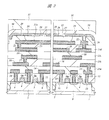
本実施の形態は、本発明をデジタル回路、センサ信号を増幅するアンプや無線送受信回路等のアナログ回路、MONOS(Metal Oxide Nitride Oxide Semiconductor)型のフラッシュメモリ回路、静電容量型圧力センサ等を1チップに混載した圧力センサ混載半導体装置に適用したものである。
本実施の形態は、本発明をデジタル回路、センサ信号を増幅するアンプや無線送受信回路等のアナログ回路、MONOS(Metal Oxide Nitride Oxide Semiconductor)型のフラッシュメモリ回路、静電容量型圧力センサ等を1チップに混載した圧力センサ混載半導体装置に適用したものである。
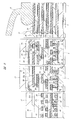
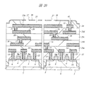
本実施の形態は、デジタル回路、センサ信号を増幅するアンプや無線送受信回路などのアナログ回路、EEPROM(Electrically Erasable and Programmable Read Only Memory)回路、静電容量型圧力センサなどを1チップに混載した圧力センサ混載半導体装置に適用したものである。
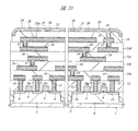
本実施の形態は、デジタル回路、センサ信号を増幅するアンプや無線送受信回路などのアナログ回路、EEPROM回路、静電容量型圧力センサなどを1チップに混載した圧力センサ混載半導体装置に適用したものである。
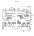
図39は、本実施の形態による圧力検知部の断面図である。本実施の形態では、第4層配線20が最上層配線であり、その上部には平坦化された酸化シリコン膜58が形成されており、酸化シリコン膜59の上部には、窒化シリコン膜59が形成されている。また、窒化シリコン膜59の上部には、最上層配線よりも上層の導電層で構成された電極91が形成されている。電極91は、例えばアルミニウム合金膜などからなり、ヴィアホール92を通じて第4層配線20に接続されている。
2 素子分離溝
3 ゲート酸化膜
4 ゲート電極
4a ポリサイド膜
5 キャップ絶縁膜
6 サイドウォール
7 p型ウエル
8 n型ウエル
9 拡散層(ソース、ドレイン)
10 拡散層(ソース、ドレイン)
11 酸化シリコン膜
12 コンタクトホール
13 プラグ
14 第1層配線
15 ヴィアホール
16 第2層配線
17 ヴィアホール
18 第3層配線
19 ヴィアホール
20 第4層配線
21 ヴィアホール
22 第5層配線
22a、22b 下部電極
23 層間絶縁膜
24 酸化シリコン膜
25 空洞
26 タングステンシリサイド膜
27 孔
28 窒化シリコン膜
29 酸化シリコン膜
30 窒化シリコン膜
31 感光性ポリイミド膜
32 開口
33 金ワイヤ
34 接続部
35 端部
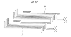
36、37 電源配線
39 タングステン膜
40 メモリゲート
41 制御ゲート
42 ONO膜
43 サイドウォール
44 キャップ絶縁膜
45 ヴィアホール
46、47 酸化シリコン膜
50 パッド
51 パッド
52 引き出し配線
53 窒化シリコン膜
54、55、56 酸化シリコン膜
57 下部電極
58 酸化シリコン膜
59 窒化シリコン膜
60 圧力センサ混載半導体装置
61 ダイパッド部
62 リード
63 筒
64 モールド樹脂
65 シリコーン樹脂
66 樹脂膜
67 パッケージ
70 プリント回路基板
71 ボタン電池
72 端子
73 水晶振動子
74 受動素子
76 プリント回路基板
77 ボタン電池
78 端子
79 パッケージ
80 パッケージ
81 シリコン基板
82 酸化シリコン膜
83 窒化シリコン膜
84 下部電極
85 ダイヤフラム
86 孔
87 窒化シリコン膜
88 酸化シリコン膜
89 層間絶縁膜
90 開口部
91 電極
91a〜91d 電極
92 ヴィアホール
93 感圧導電膜
94 アルミニウム合金膜
Qn、Qp MOSトランジスタ
Qf MONOS型フラッシュメモリトランジスタ
Claims (9)
- 半導体基板上に設けられるMOSトランジスタと、前記半導体基板の上方に設けられる多層配線とを備える電子回路と、
固定電極と、前記固定電極の上方に設けられるダイアフラムと、前記固定電極と前記ダイアフラムの間に設けられる空洞とを備えるセンサと、を有し、
前記固定電極は、前記多層配線のうち最上層の配線を用いて形成され、
前記ダイアフラムは、前記最上層の配線よりも上方のタングステンシリサイド膜またはタングステン膜からなる導電層を用いて形成され、
前記タングステンシリサイド膜またはタングステン膜は引っ張り応力を有することを特徴とする半導体装置。 - 前記センサの少なくとも一部が、前記電子回路と重なる平面領域内の前記電子回路よりも上層に配置されていることを特徴とする請求項1記載の半導体装置。
- 前記電子回路は、アナログ、デジタル混載回路と不揮発メモリ回路とを含むことを特徴とする請求項1記載の半導体装置。
- 前記センサは、前記固定電極と前記ダイアフラムの間の静電容量を測定することにより圧力を検知することを特徴とする請求項1記載の半導体装置。
- タイヤ内に設置され、前記タイヤ内の圧力の検知に用いられることを特徴とする請求項1記載の半導体装置。
- 前記センサは、圧力センサであることを特徴とする請求項1記載の半導体装置。
- 前記センサは、静電容量型圧力センサであることを特徴とする請求項1記載の半導体装置。
- 半導体基板上に設けられるMOSトランジスタと、前記半導体基板の上方に設けられる多層配線とを備える電子回路と、
固定電極と、前記固定電極の上方に設けられるダイアフラムと、前記固定電極と前記ダイアフラムの間に設けられる空洞とを備えるセンサと、を有し、
前記固定電極は、前記多層配線のうち最上層の配線を用いて形成され、
前記ダイアフラムは、前記最上層の配線よりも上方の導電層を用いて形成され、
前記電子回路は、デジタル回路とアナログ回路とを有し、
前記センサは、前記デジタル回路の形成領域上に形成され、前記アナログ回路の形成領域上には形成されないことを特徴とする半導体装置。 - 半導体基板上に設けられるMOSトランジスタと、前記半導体基板の上方に設けられる多層配線とを備える電子回路と、
固定電極と、前記固定電極の上方に設けられるダイアフラムと、前記固定電極と前記ダイアフラムの間に設けられる空洞とを備えるセンサと、を有する半導体装置の製造方法であって、
前記固定電極を、前記多層配線のうち最上層の配線を用いて形成し、
前記ダイアフラムを、前記最上層の配線よりも上方のタングステンシリサイド膜またはタングステン膜からなる導電層を用いて形成し、
前記タングステンシリサイド膜またはタングステン膜は引っ張り応力を有することを特徴とする半導体装置の製造方法。
Priority Applications (3)
| Application Number | Priority Date | Filing Date | Title |
|---|---|---|---|
| US11/237,897 US7270012B2 (en) | 2004-10-01 | 2005-09-29 | Semiconductor device embedded with pressure sensor and manufacturing method thereof |
| JP2005284013A JP5280609B2 (ja) | 2004-10-01 | 2005-09-29 | 半導体装置およびその製造方法 |
| US11/878,243 US7451656B2 (en) | 2004-10-01 | 2007-07-23 | Semiconductor device embedded with pressure sensor and manufacturing method thereof |
Applications Claiming Priority (3)
| Application Number | Priority Date | Filing Date | Title |
|---|---|---|---|
| JP2004289476 | 2004-10-01 | ||
| JP2004289476 | 2004-10-01 | ||
| JP2005284013A JP5280609B2 (ja) | 2004-10-01 | 2005-09-29 | 半導体装置およびその製造方法 |
Publications (2)
| Publication Number | Publication Date |
|---|---|
| JP2006126182A JP2006126182A (ja) | 2006-05-18 |
| JP5280609B2 true JP5280609B2 (ja) | 2013-09-04 |
Family
ID=36124241
Family Applications (1)
| Application Number | Title | Priority Date | Filing Date |
|---|---|---|---|
| JP2005284013A Expired - Fee Related JP5280609B2 (ja) | 2004-10-01 | 2005-09-29 | 半導体装置およびその製造方法 |
Country Status (2)
| Country | Link |
|---|---|
| US (2) | US7270012B2 (ja) |
| JP (1) | JP5280609B2 (ja) |
Families Citing this family (40)
| Publication number | Priority date | Publication date | Assignee | Title |
|---|---|---|---|---|
| US7722434B2 (en) * | 2005-03-29 | 2010-05-25 | Kla-Tencor Corporation | Apparatus for measurement of parameters in process equipment |
| JP4988217B2 (ja) * | 2006-02-03 | 2012-08-01 | 株式会社日立製作所 | Mems構造体の製造方法 |
| CN101460321B (zh) * | 2006-04-25 | 2011-07-20 | 普利司通美国轮胎运营有限责任公司 | 具有无线微米和纳米传感器系统的弹性体 |
| JP4352271B2 (ja) * | 2006-06-09 | 2009-10-28 | セイコーエプソン株式会社 | 半導体装置 |
| US7698952B2 (en) | 2006-10-03 | 2010-04-20 | Kla-Tencor Corporation | Pressure sensing device |
| JP4337870B2 (ja) | 2006-12-15 | 2009-09-30 | セイコーエプソン株式会社 | Memsレゾネータ及びmemsレゾネータの製造方法 |
| JP4967907B2 (ja) * | 2007-08-01 | 2012-07-04 | ミツミ電機株式会社 | 半導体圧力センサ及びその製造方法 |
| TWI333933B (en) * | 2007-08-17 | 2010-12-01 | Advanced Semiconductor Eng | Microelectromechanical-system package and method for manufacturing the same |
| JP5055097B2 (ja) * | 2007-11-08 | 2012-10-24 | 日東電工株式会社 | 検査用粘着シート |
| JP4655083B2 (ja) | 2007-11-16 | 2011-03-23 | セイコーエプソン株式会社 | 微小電気機械装置 |
| US8258591B2 (en) * | 2008-01-16 | 2012-09-04 | Solid State System Co., Ltd. | Micro-electro-mechanical systems (MEMS) device |
| JP4705964B2 (ja) * | 2008-02-21 | 2011-06-22 | 株式会社日立製作所 | 半導体装置 |
| US8217475B2 (en) * | 2008-05-15 | 2012-07-10 | Custom Sensors & Technologies, Inc. | Backside controlled MEMS capacitive sensor and interface and method |
| US8456625B2 (en) * | 2008-07-30 | 2013-06-04 | International Business Machines Corporation | Methods for real-time contamination, environmental, or physical monitoring of a photomask |
| US8136055B2 (en) * | 2008-07-30 | 2012-03-13 | International Business Machines Corporation | Systems for real-time contamination, environmental, or physical monitoring of a photomask |
| JP4947065B2 (ja) * | 2009-01-09 | 2012-06-06 | セイコーエプソン株式会社 | Memsレゾネータの製造方法 |
| DE102009000514A1 (de) * | 2009-01-30 | 2010-08-26 | Robert Bosch Gmbh | Verbundbauteil sowie Verfahren zum Herstellen eines Verbundbauteil |
| US8724339B2 (en) | 2009-12-01 | 2014-05-13 | Apple Inc. | Compact media player |
| JP5436404B2 (ja) * | 2010-12-17 | 2014-03-05 | 三菱電機株式会社 | 半導体圧力センサ及びその製造方法 |
| DE102011005676A1 (de) * | 2011-03-17 | 2012-09-20 | Robert Bosch Gmbh | Bauteil |
| FR2974800B1 (fr) * | 2011-05-05 | 2013-04-26 | Saint Gobain | Substrat transparent revetu d'un empilement de couches minerales dont une poreuse recouverte |
| US9209091B1 (en) | 2011-08-05 | 2015-12-08 | Maxim Integrated Products, Inc. | Integrated monolithic galvanic isolator |
| US9021887B2 (en) | 2011-12-19 | 2015-05-05 | Infineon Technologies Ag | Micromechanical semiconductor sensing device |
| JP2013156066A (ja) * | 2012-01-27 | 2013-08-15 | Wacom Co Ltd | 静電容量方式圧力センシング半導体デバイス |
| JP5914010B2 (ja) | 2012-01-30 | 2016-05-11 | ルネサスエレクトロニクス株式会社 | 半導体集積回路装置の製造方法 |
| JP5892595B2 (ja) | 2012-02-06 | 2016-03-23 | 株式会社ワコム | 位置指示器 |
| EP2637007B1 (en) * | 2012-03-08 | 2020-01-22 | ams international AG | MEMS capacitive pressure sensor |
| EP2657691B1 (de) * | 2012-04-25 | 2018-08-29 | E+E Elektronik Ges.m.b.H. | Feuchtesensor-Anordnung |
| JP5761126B2 (ja) * | 2012-05-31 | 2015-08-12 | 日本精機株式会社 | 圧力検出装置 |
| FR3000841A1 (fr) * | 2013-01-09 | 2014-07-11 | St Microelectronics Rousset | Procede de realisation d'un dispositif metallique loge dans un logement ferme au sein d'un circuit integre, et circuit integre correspondant |
| KR20150033415A (ko) * | 2013-09-24 | 2015-04-01 | 삼성전기주식회사 | 터치센서 모듈 |
| US9129956B2 (en) * | 2013-12-11 | 2015-09-08 | Taiwan Semiconductor Manufacturing Company, Ltd. | Device having multiple-layer pins in memory MUX1 layout |
| FR3022691B1 (fr) | 2014-06-23 | 2016-07-01 | Stmicroelectronics Rousset | Dispositif capacitif commandable integre |
| JP2016095284A (ja) * | 2014-11-17 | 2016-05-26 | セイコーエプソン株式会社 | 電子デバイス、物理量センサー、圧力センサー、高度計、電子機器および移動体 |
| US9466452B1 (en) | 2015-03-31 | 2016-10-11 | Stmicroelectronics, Inc. | Integrated cantilever switch |
| FR3034567B1 (fr) | 2015-03-31 | 2017-04-28 | St Microelectronics Rousset | Dispositif metallique a piece(s) mobile(s) ameliore loge dans une cavite de la partie d'interconnexion (" beol ") d'un circuit integre |
| KR20160143029A (ko) * | 2015-06-04 | 2016-12-14 | 엘지전자 주식회사 | 이동 단말기 |
| US10505255B2 (en) * | 2017-01-30 | 2019-12-10 | Infineon Technologies Ag | Radio frequency device packages and methods of formation thereof |
| KR102322257B1 (ko) * | 2017-05-11 | 2021-11-04 | 현대자동차 주식회사 | 마이크로폰 및 그 제조 방법 |
| WO2020086532A1 (en) * | 2018-10-22 | 2020-04-30 | Thin Film Electronics Asa | Barrier stacks for printed and/or thin film electronics methods of manufacturing the same, and method of controlling a threshold voltage of a thin film transistor |
Family Cites Families (24)
| Publication number | Priority date | Publication date | Assignee | Title |
|---|---|---|---|---|
| US3922705A (en) * | 1973-06-04 | 1975-11-25 | Gen Electric | Dielectrically isolated integral silicon diaphram or other semiconductor product |
| US4158807A (en) * | 1977-04-25 | 1979-06-19 | Massachusetts Institute Of Technology | Gapped gate charge-flow transistor with a thin film sensor having two modes of conduction within the gapped gate used to sense a property of the ambient environment |
| JPS5427394A (en) * | 1977-08-02 | 1979-03-01 | Seiko Epson Corp | Multi-layer liquid crystal panel |
| CA1314410C (en) * | 1986-12-08 | 1993-03-16 | Masanori Nishiguchi | Wiring structure of semiconductor pressure sensor |
| US4823605A (en) * | 1987-03-18 | 1989-04-25 | Siemens Aktiengesellschaft | Semiconductor pressure sensor with casing and method for its manufacture |
| JPH0465643A (ja) * | 1990-07-05 | 1992-03-02 | Mitsubishi Electric Corp | 半導体圧力センサ及びその製造方法 |
| US5391502A (en) * | 1993-08-27 | 1995-02-21 | Vlsi Technology, Inc. | Per-wafer method for globally stressing gate oxide during device fabrication |
| DE4418207C1 (de) | 1994-05-25 | 1995-06-22 | Siemens Ag | Thermischer Sensor/Aktuator in Halbleitermaterial |
| JPH0917276A (ja) | 1995-06-29 | 1997-01-17 | Inaba Gomme Kk | 感圧センサー |
| WO1997019468A1 (en) * | 1995-11-20 | 1997-05-29 | Hitachi, Ltd. | Semiconductor storage device and process for manufacturing the same |
| JPH1013018A (ja) * | 1996-06-21 | 1998-01-16 | Denso Corp | 多層基板 |
| DE19626081A1 (de) * | 1996-06-28 | 1998-01-02 | Siemens Ag | Halbleiter-Bauelement |
| JP4655252B2 (ja) | 1999-04-15 | 2011-03-23 | 新原 ▲晧▼一 | 変形導電性エラストマーの製造方法 |
| SG87046A1 (en) * | 1999-08-17 | 2002-03-19 | Micron Technology Inc | Multi-chip module with stacked dice |
| JP4047506B2 (ja) * | 2000-02-01 | 2008-02-13 | 日本電気株式会社 | 化学センサカートリッジ及びそれを備えた化学センサ並びにそれを用いた試料の測定方法 |
| JP3507978B2 (ja) * | 2000-02-23 | 2004-03-15 | 株式会社日立製作所 | 静電容量式圧力センサー |
| US6472243B2 (en) | 2000-12-11 | 2002-10-29 | Motorola, Inc. | Method of forming an integrated CMOS capacitive pressure sensor |
| JP3745648B2 (ja) * | 2001-06-06 | 2006-02-15 | 日本電信電話株式会社 | 微細構造の製造方法 |
| JP4794073B2 (ja) * | 2001-06-28 | 2011-10-12 | 京セラ株式会社 | 圧力検出装置用パッケージ |
| JP2004200645A (ja) * | 2002-10-23 | 2004-07-15 | Oki Electric Ind Co Ltd | 半導体素子のゲートマスク製造方法 |
| JP4437388B2 (ja) * | 2003-02-06 | 2010-03-24 | 株式会社リコー | 半導体装置 |
| JP2004268746A (ja) * | 2003-03-10 | 2004-09-30 | Bridgestone Corp | 車輪装着起電力発生装置、およびこれを用いた表示装置ならびに温度異常検出装置 |
| JP2004309282A (ja) * | 2003-04-07 | 2004-11-04 | Denso Corp | 容量式圧力センサ |
| JP2005045112A (ja) * | 2003-07-24 | 2005-02-17 | Matsushita Electric Ind Co Ltd | 部品内蔵フレキシブル回路基板およびその製造方法 |
-
2005
- 2005-09-29 JP JP2005284013A patent/JP5280609B2/ja not_active Expired - Fee Related
- 2005-09-29 US US11/237,897 patent/US7270012B2/en not_active Expired - Lifetime
-
2007
- 2007-07-23 US US11/878,243 patent/US7451656B2/en not_active Expired - Lifetime
Also Published As
| Publication number | Publication date |
|---|---|
| US20070262401A1 (en) | 2007-11-15 |
| US7451656B2 (en) | 2008-11-18 |
| US20060070449A1 (en) | 2006-04-06 |
| JP2006126182A (ja) | 2006-05-18 |
| US7270012B2 (en) | 2007-09-18 |
Similar Documents
| Publication | Publication Date | Title |
|---|---|---|
| JP2006126182A (ja) | 圧力センサ混載半導体装置およびその製造方法 | |
| US11692892B2 (en) | MEMS pressure sensor and method for forming the same | |
| TWI622759B (zh) | MEMS pressure sensor and method of forming same | |
| US7919814B2 (en) | Semiconductor device with integrated circuit electrically connected to a MEMS sensor by a through-electrode | |
| US8227877B2 (en) | Semiconductor bio-sensors and methods of manufacturing the same | |
| US6713828B1 (en) | Monolithic fully-integrated vacuum sealed BiCMOS pressure sensor | |
| US9949037B2 (en) | MEMS microphone and method for forming the same | |
| US8393223B2 (en) | Pressure sensor with resistance strain gages | |
| US8199963B2 (en) | Microphone arrangement and method for production thereof | |
| US20110121908A1 (en) | Mems Resonator and Manufacturing Method of the Same | |
| CN111854976A (zh) | 红外热堆传感器及其制作方法 | |
| CN100515922C (zh) | 具有隔膜的传感器以及制作它的方法 | |
| JP2017215224A (ja) | 半導体圧力センサ | |
| US7342263B2 (en) | Circuit device | |
| JP3567094B2 (ja) | 回路内蔵型センサおよびそれを用いた圧力検出装置 | |
| JP4705964B2 (ja) | 半導体装置 | |
| US20100218613A1 (en) | Semiconductor device including a cavity | |
| JP6119615B2 (ja) | 半導体装置の製造方法 | |
| EP2796844B1 (en) | Mems capacitive pressure sensor | |
| EP2492240A1 (en) | IC with pressure sensor and manufacturing method thereof | |
| CN112687674A (zh) | 一种红外热堆传感器的封装结构及方法 | |
| JPH04299871A (ja) | 半導体圧力センサおよびその製造方法 | |
| CN213905357U (zh) | 一种红外热堆传感器的封装结构 | |
| JP3463489B2 (ja) | 半導体圧力感知装置及びその製造方法 | |
| JP6541066B2 (ja) | 圧力センサ |
Legal Events
| Date | Code | Title | Description |
|---|---|---|---|
| A621 | Written request for application examination |
Free format text: JAPANESE INTERMEDIATE CODE: A621 Effective date: 20080808 |
|
| A131 | Notification of reasons for refusal |
Free format text: JAPANESE INTERMEDIATE CODE: A131 Effective date: 20110906 |
|
| A521 | Request for written amendment filed |
Free format text: JAPANESE INTERMEDIATE CODE: A523 Effective date: 20111101 |
|
| A131 | Notification of reasons for refusal |
Free format text: JAPANESE INTERMEDIATE CODE: A131 Effective date: 20120417 |
|
| A521 | Request for written amendment filed |
Free format text: JAPANESE INTERMEDIATE CODE: A523 Effective date: 20120615 |
|
| A02 | Decision of refusal |
Free format text: JAPANESE INTERMEDIATE CODE: A02 Effective date: 20121120 |
|
| A521 | Request for written amendment filed |
Free format text: JAPANESE INTERMEDIATE CODE: A523 Effective date: 20130219 |
|
| A911 | Transfer to examiner for re-examination before appeal (zenchi) |
Free format text: JAPANESE INTERMEDIATE CODE: A911 Effective date: 20130226 |
|
| TRDD | Decision of grant or rejection written | ||
| A01 | Written decision to grant a patent or to grant a registration (utility model) |
Free format text: JAPANESE INTERMEDIATE CODE: A01 Effective date: 20130430 |
|
| A61 | First payment of annual fees (during grant procedure) |
Free format text: JAPANESE INTERMEDIATE CODE: A61 Effective date: 20130523 |
|
| R150 | Certificate of patent or registration of utility model |
Free format text: JAPANESE INTERMEDIATE CODE: R150 Ref document number: 5280609 Country of ref document: JP Free format text: JAPANESE INTERMEDIATE CODE: R150 |
|
| LAPS | Cancellation because of no payment of annual fees |