JP5296423B2 - 光走査装置、画像形成装置、表示装置及び入力装置 - Google Patents
光走査装置、画像形成装置、表示装置及び入力装置 Download PDFInfo
- Publication number
- JP5296423B2 JP5296423B2 JP2008160943A JP2008160943A JP5296423B2 JP 5296423 B2 JP5296423 B2 JP 5296423B2 JP 2008160943 A JP2008160943 A JP 2008160943A JP 2008160943 A JP2008160943 A JP 2008160943A JP 5296423 B2 JP5296423 B2 JP 5296423B2
- Authority
- JP
- Japan
- Prior art keywords
- substrate
- swinging
- swing
- torsion spring
- optical scanning
- Prior art date
- Legal status (The legal status is an assumption and is not a legal conclusion. Google has not performed a legal analysis and makes no representation as to the accuracy of the status listed.)
- Expired - Fee Related
Links
- 230000003287 optical effect Effects 0.000 title claims abstract description 53
- 239000000758 substrate Substances 0.000 claims abstract description 69
- 238000009966 trimming Methods 0.000 claims description 14
- 238000001514 detection method Methods 0.000 claims description 12
- 238000012937 correction Methods 0.000 claims description 11
- 239000002184 metal Substances 0.000 claims description 9
- 238000003860 storage Methods 0.000 claims description 5
- 230000010356 wave oscillation Effects 0.000 abstract 3
- 230000010355 oscillation Effects 0.000 abstract 1
- 238000000034 method Methods 0.000 description 18
- 238000004519 manufacturing process Methods 0.000 description 12
- 238000010586 diagram Methods 0.000 description 10
- 238000012360 testing method Methods 0.000 description 9
- 239000000463 material Substances 0.000 description 8
- 238000012545 processing Methods 0.000 description 8
- 238000005516 engineering process Methods 0.000 description 6
- 238000004364 calculation method Methods 0.000 description 3
- 238000013461 design Methods 0.000 description 2
- 238000006073 displacement reaction Methods 0.000 description 2
- 238000002474 experimental method Methods 0.000 description 2
- 229910021421 monocrystalline silicon Inorganic materials 0.000 description 2
- 238000004080 punching Methods 0.000 description 2
- 239000004065 semiconductor Substances 0.000 description 2
- 239000011248 coating agent Substances 0.000 description 1
- 238000000576 coating method Methods 0.000 description 1
- 230000008602 contraction Effects 0.000 description 1
- 230000006866 deterioration Effects 0.000 description 1
- 238000011161 development Methods 0.000 description 1
- 238000005530 etching Methods 0.000 description 1
- 230000005484 gravity Effects 0.000 description 1
- 239000000696 magnetic material Substances 0.000 description 1
- 238000005459 micromachining Methods 0.000 description 1
- 238000000206 photolithography Methods 0.000 description 1
- 230000000704 physical effect Effects 0.000 description 1
- 238000003825 pressing Methods 0.000 description 1
- 230000003068 static effect Effects 0.000 description 1
- 238000001771 vacuum deposition Methods 0.000 description 1
Images


Landscapes
- Mechanical Optical Scanning Systems (AREA)
Description
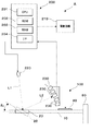
図1は本発明の第1実施形態に係る光走査装置Aのブロック図である。光走査装置Aは走査ユニット100と、制御ユニット200と、駆動回路210と、テスト用光源220と、受光器230と、を備える。まず、走査ユニット100の構成について説明する。図2は走査ユニット100の斜視図、図3は走査ユニット100の動作説明図である。
f=2π√(k/I)
で表される。共振周波数は、揺動部材20の慣性モーメントIや捩りばね部材30のばね定数kに大きく依存しており、これらは部材の物性のみならず、形状にも大きく依存する。
θ=θmax・sinω(t+(T2/4−T1/2))
ω=2π/T2
と表せる。そして、
t=0、θ=θα(又は、t=T1、θ=θα)
であるから、θmaxを演算できる。
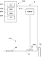
本実施形態では、周囲温度の変化に起因する揺動部材20の揺動態様の変化を自動較正するものである。図7は本発明の第2実施形態に係る光走査装置Bのブロック図である。上記第1実施形態の光走査装置Aと同様の構成については同じ符号を付して説明を割愛し、異なる構成についてのみ説明する。
次に、走査ユニット100の他の実施形態について説明する。本実施形態では、基板10又は揺動部材20の少なくともいずれか一方に、トリミング用の突出片部を設ける。そして、製造誤差は、突出片部をトリミングすることにより較正する。
本発明の光走査装置は、例えば、レーザビームプリンタ等の画像形成装置、ヘッドマウントディスプレイ等の画像表示装置、バーコードリーダ等の入力装置等の各種装置に適用可能である。また、本発明の光走査装置により2次元スキャナを構成した平板ディスプレイや、読取センサに対する原稿走査用光スキャナへの応用も可能である。その場合、上記第1及び第2実施形態の制御ユニット200は、適用先の装置の制御ユニットで兼用してもよい。
10 基板
20 揺動部材
21 光反射面
30 捩りばね部材
100 走査ユニット
Claims (12)
- 基板と、
前記基板に板波振動を励起する駆動手段と、
前記基板に連結された捩りばね部材と、
前記捩りばね部材に連結され、前記基板の板波振動により励起される前記捩りばね部材の捩れ振動により、前記捩りばね部材を揺動中心軸として揺動する揺動部材と、
前記揺動部材に形成された光反射面と、
前記光反射面に光を投射する光源と、
前記光反射面で反射された反射光を受光する受光手段と、
前記受光手段の受光結果に基づいて、前記揺動部材の揺動態様が目的とする揺動態様となるように、前記駆動手段の駆動条件を補正する補正手段と、を備え、
前記基板と、前記捩りばね部材と、前記揺動部材とが、1枚の金属板から一体的に形成され、
前記基板が、トリミング用の突出片部を有することを特徴とする光走査装置。 - 前記受光手段は、
前記揺動部材が予め定めた振れ角に位置したときに前記反射光を受光する位置に配置され、
前記補正手段は、
前記受光手段による前記反射光の受光間隔に基づいて前記駆動条件を補正することを特徴とする請求項1に記載の光走査装置。 - 前記揺動態様が、前記揺動部材の最大振れ角であることを特徴とする請求項1又は2に記載の光走査装置。
- 基板と、
前記基板に板波振動を励起する駆動手段と、
前記基板に連結された捩りばね部材と、
前記捩りばね部材に連結され、前記基板の板波振動により励起される前記捩りばね部材の捩れ振動により、前記捩りばね部材を揺動中心軸として揺動する揺動部材と、
前記揺動部材に形成された光反射面と、
周囲温度を検出する温度検出手段と、
複数の周囲温度について、前記揺動部材の揺動態様を目的とする揺動態様とするための前記駆動手段の駆動条件に関するデータを記憶した記憶手段と、
前記温度検出手段の検出結果と、前記記憶手段に記憶した前記データとに基づいて、前記駆動手段の駆動条件を設定する設定手段と、を備え、
前記基板と、前記捩りばね部材と、前記揺動部材とが、1枚の金属板から一体的に形成され、
前記基板が、トリミング用の突出片部を有することを特徴とする光走査装置。 - 前記駆動手段が圧電体であり、
前記駆動条件が、前記圧電体の駆動電圧を少なくとも含むことを特徴とする請求項1乃至4のいずれか1項に記載の光走査装置。 - 前記駆動手段が圧電体であり、
前記駆動条件が、前記圧電体の駆動周波数を少なくとも含むことを特徴とする請求項1乃至5のいずれか1項に記載の光走査装置。 - 前記基板及び前記揺動部材が、それぞれ前記突出片部を有し、
前記光反射面は、前記突出片部には形成されていないことを特徴とする請求項1乃至6のいずれか1項に記載の光走査装置。 - 前記基板を支持する支持部材を備え、
前記基板は、自由端である一方端部と、前記支持部材に支持される他方端部と、を有し、
前記基板の前記突出片部は、前記自由端側に設けられていることを特徴とする請求項1乃至7のいずれか1項に記載の光走査装置。 - 前記基板は、前記自由端側に互いに離間する一対のアーム部を有し、
前記ねじりばね部材は一対設けられ、それぞれ、前記アーム部と前記揺動部材とを連結し、
前記基板の前記突出片部は、各々の前記アーム部の先端に設けられていることを特徴とする請求項8に記載の光走査装置。 - 請求項1乃至9のいずれか1項に記載の光走査装置を備えたことを特徴とする画像形成装置。
- 請求項1乃至9のいずれか1項に記載の光走査装置を備えたことを特徴とする表示装置。
- 請求項1乃至9のいずれか1項に記載の光走査装置を備えたことを特徴とする入力装置。
Priority Applications (1)
| Application Number | Priority Date | Filing Date | Title |
|---|---|---|---|
| JP2008160943A JP5296423B2 (ja) | 2008-06-19 | 2008-06-19 | 光走査装置、画像形成装置、表示装置及び入力装置 |
Applications Claiming Priority (1)
| Application Number | Priority Date | Filing Date | Title |
|---|---|---|---|
| JP2008160943A JP5296423B2 (ja) | 2008-06-19 | 2008-06-19 | 光走査装置、画像形成装置、表示装置及び入力装置 |
Publications (2)
| Publication Number | Publication Date |
|---|---|
| JP2010002636A JP2010002636A (ja) | 2010-01-07 |
| JP5296423B2 true JP5296423B2 (ja) | 2013-09-25 |
Family
ID=41584421
Family Applications (1)
| Application Number | Title | Priority Date | Filing Date |
|---|---|---|---|
| JP2008160943A Expired - Fee Related JP5296423B2 (ja) | 2008-06-19 | 2008-06-19 | 光走査装置、画像形成装置、表示装置及び入力装置 |
Country Status (1)
| Country | Link |
|---|---|
| JP (1) | JP5296423B2 (ja) |
Families Citing this family (6)
| Publication number | Priority date | Publication date | Assignee | Title |
|---|---|---|---|---|
| JP5282753B2 (ja) * | 2010-03-29 | 2013-09-04 | ブラザー工業株式会社 | 圧電アクチュエータ、光スキャナ、光走査型画像表示装置、画像形成装置 |
| JP2012037832A (ja) * | 2010-08-11 | 2012-02-23 | Shinano Kenshi Co Ltd | 光走査装置 |
| JP6270378B2 (ja) * | 2012-08-27 | 2018-01-31 | キヤノン電子株式会社 | 揺動素子、アクチュエータ装置、及び光走査装置 |
| JP6480784B2 (ja) * | 2015-04-02 | 2019-03-13 | 日本信号株式会社 | 光走査アクチュエータの評価装置 |
| JP2021089405A (ja) * | 2019-12-06 | 2021-06-10 | セイコーエプソン株式会社 | 光走査装置、三次元計測装置、及び、ロボットシステム |
| JP2022021617A (ja) * | 2020-07-22 | 2022-02-03 | セイコーエプソン株式会社 | 距離計測装置およびロボット |
Family Cites Families (13)
| Publication number | Priority date | Publication date | Assignee | Title |
|---|---|---|---|---|
| JPH0749462A (ja) * | 1993-08-04 | 1995-02-21 | Nikon Corp | 共振スキャナ |
| JPH07181415A (ja) * | 1993-12-22 | 1995-07-21 | Omron Corp | 光走査装置 |
| JPH08240782A (ja) * | 1995-03-02 | 1996-09-17 | Omron Corp | 光スキャナ、光センサ装置及び符号情報読み取り装置並びに符号情報読み取り方法 |
| JP3518099B2 (ja) * | 1995-10-06 | 2004-04-12 | 株式会社デンソー | 光スキャナ装置 |
| JP4390174B2 (ja) * | 2001-09-14 | 2009-12-24 | 株式会社リコー | 光走査装置 |
| JP2003215493A (ja) * | 2002-01-28 | 2003-07-30 | Nippon Signal Co Ltd:The | 光走査装置 |
| JP2006178408A (ja) * | 2004-11-25 | 2006-07-06 | Ricoh Co Ltd | スキャナ素子、光走査装置および画像形成装置 |
| JP2006230048A (ja) * | 2005-02-15 | 2006-08-31 | Seiko Epson Corp | アクチュエータの共振周波数の調整方法およびアクチュエータ |
| US8125699B2 (en) * | 2006-09-27 | 2012-02-28 | National Institute Of Advanced Industrial Science And Technology | Optical scanning device |
| US8305669B2 (en) * | 2006-10-12 | 2012-11-06 | National Institute Of Advanced Industrial Science And Technology | Optical scanning device |
| JP2009175513A (ja) * | 2008-01-25 | 2009-08-06 | Panasonic Corp | 振動ミラーおよびレーザスキャニングユニット |
| JP2010002454A (ja) * | 2008-06-18 | 2010-01-07 | Panasonic Corp | 光走査装置 |
| JP2010002455A (ja) * | 2008-06-18 | 2010-01-07 | Panasonic Corp | 光走査装置 |
-
2008
- 2008-06-19 JP JP2008160943A patent/JP5296423B2/ja not_active Expired - Fee Related
Also Published As
| Publication number | Publication date |
|---|---|
| JP2010002636A (ja) | 2010-01-07 |
Similar Documents
| Publication | Publication Date | Title |
|---|---|---|
| JP5296423B2 (ja) | 光走査装置、画像形成装置、表示装置及び入力装置 | |
| US8422109B2 (en) | Optical reflection element | |
| US7659918B2 (en) | Apparatus and methods for adjusting the rotational frequency of a scanning device | |
| US7446920B2 (en) | Optical deflector and optical instrument using the same | |
| US7355774B2 (en) | Optical deflector and optical apparatus using the same | |
| CN101086555B (zh) | 振荡器装置、光偏转器以及使用光偏转器的光学器械 | |
| US20100014142A1 (en) | Optical scanning device | |
| JP2011180322A (ja) | 光スキャナ、光スキャナ制御方法、及び光スキャナを用いた画像表示装置。 | |
| JP2015070214A (ja) | 光学装置、投影光学系、露光装置および物品の製造方法 | |
| CN101551518B (zh) | 可移动体设备和使用该可移动体设备的光偏转器 | |
| US8520282B2 (en) | Optical scanning apparatus configured to deflect and scan laser beam by using MEMS mirror | |
| JP5296424B2 (ja) | 光走査装置、画像形成装置、表示装置及び入力装置 | |
| JP2009031643A (ja) | 揺動体装置、光偏向器およびそれを用いた画像形成装置 | |
| JP2008145839A (ja) | 光スキャナ装置 | |
| JP2012194283A (ja) | 光偏向装置、光走査装置、画像形成装置及び画像投影装置 | |
| JP2006081320A (ja) | アクチュエータ | |
| JP2010014871A (ja) | 揺動体装置、光偏向装置、光学機器、及び共振周波数検出方法 | |
| JP2008225041A (ja) | 光スキャナ駆動制御方法及び駆動制御装置 | |
| JP2006075944A (ja) | アクチュエータ | |
| JP6231361B2 (ja) | 振動素子および光走査装置 | |
| JP5451047B2 (ja) | 光学走査装置 | |
| JP2995836B2 (ja) | 光走査装置 | |
| JP2011137871A (ja) | 光学走査装置及び画像形成装置 | |
| JP6104063B2 (ja) | 光走査装置、画像形成装置および映像投射装置 | |
| JP6301184B2 (ja) | 振動素子、光走査装置、画像形成装置、画像投影装置および光学パターン読み取り装置 |
Legal Events
| Date | Code | Title | Description |
|---|---|---|---|
| A621 | Written request for application examination |
Free format text: JAPANESE INTERMEDIATE CODE: A621 Effective date: 20110609 |
|
| A977 | Report on retrieval |
Free format text: JAPANESE INTERMEDIATE CODE: A971007 Effective date: 20120523 |
|
| A131 | Notification of reasons for refusal |
Free format text: JAPANESE INTERMEDIATE CODE: A131 Effective date: 20120525 |
|
| A521 | Request for written amendment filed |
Free format text: JAPANESE INTERMEDIATE CODE: A523 Effective date: 20120723 |
|
| A131 | Notification of reasons for refusal |
Free format text: JAPANESE INTERMEDIATE CODE: A131 Effective date: 20130107 |
|
| A521 | Request for written amendment filed |
Free format text: JAPANESE INTERMEDIATE CODE: A523 Effective date: 20130225 |
|
| TRDD | Decision of grant or rejection written | ||
| A01 | Written decision to grant a patent or to grant a registration (utility model) |
Free format text: JAPANESE INTERMEDIATE CODE: A01 Effective date: 20130524 |
|
| A61 | First payment of annual fees (during grant procedure) |
Free format text: JAPANESE INTERMEDIATE CODE: A61 Effective date: 20130613 |
|
| R150 | Certificate of patent or registration of utility model |
Ref document number: 5296423 Country of ref document: JP Free format text: JAPANESE INTERMEDIATE CODE: R150 Free format text: JAPANESE INTERMEDIATE CODE: R150 |
|
| R250 | Receipt of annual fees |
Free format text: JAPANESE INTERMEDIATE CODE: R250 |
|
| R250 | Receipt of annual fees |
Free format text: JAPANESE INTERMEDIATE CODE: R250 |
|
| R250 | Receipt of annual fees |
Free format text: JAPANESE INTERMEDIATE CODE: R250 |
|
| R250 | Receipt of annual fees |
Free format text: JAPANESE INTERMEDIATE CODE: R250 |
|
| R250 | Receipt of annual fees |
Free format text: JAPANESE INTERMEDIATE CODE: R250 |
|
| R250 | Receipt of annual fees |
Free format text: JAPANESE INTERMEDIATE CODE: R250 |
|
| R250 | Receipt of annual fees |
Free format text: JAPANESE INTERMEDIATE CODE: R250 |
|
| R250 | Receipt of annual fees |
Free format text: JAPANESE INTERMEDIATE CODE: R250 |
|
| LAPS | Cancellation because of no payment of annual fees |