JP5328533B2 - Optical connector - Google Patents

Optical connector Download PDF

Info

Publication number
JP5328533B2
JP5328533B2 JP2009162940A JP2009162940A JP5328533B2 JP 5328533 B2 JP5328533 B2 JP 5328533B2 JP 2009162940 A JP2009162940 A JP 2009162940A JP 2009162940 A JP2009162940 A JP 2009162940A JP 5328533 B2 JP5328533 B2 JP 5328533B2
Authority
JP
Japan
Prior art keywords
optical waveguide
connector
planar optical
planar
fitting
Prior art date
Legal status (The legal status is an assumption and is not a legal conclusion. Google has not performed a legal analysis and makes no representation as to the accuracy of the status listed.)
Expired - Fee Related
Application number
JP2009162940A
Other languages
Japanese (ja)
Other versions
JP2011017933A (en
Inventor
顕人 西村
幸生 林
Current Assignee (The listed assignees may be inaccurate. Google has not performed a legal analysis and makes no representation or warranty as to the accuracy of the list.)
Fujikura Ltd
Original Assignee
Fujikura Ltd
Priority date (The priority date is an assumption and is not a legal conclusion. Google has not performed a legal analysis and makes no representation as to the accuracy of the date listed.)
Filing date
Publication date
Application filed by Fujikura Ltd filed Critical Fujikura Ltd
Priority to JP2009162940A priority Critical patent/JP5328533B2/en
Publication of JP2011017933A publication Critical patent/JP2011017933A/en
Application granted granted Critical
Publication of JP5328533B2 publication Critical patent/JP5328533B2/en
Expired - Fee Related legal-status Critical Current
Anticipated expiration legal-status Critical

Links

Images

Landscapes

  • Mechanical Coupling Of Light Guides (AREA)
  • Optical Couplings Of Light Guides (AREA)
  • Optical Integrated Circuits (AREA)
  • Semiconductor Lasers (AREA)

Description

本発明は、光コネクタに係り、特に、平面型光導波路を保持する光コネクタに関する。   The present invention relates to an optical connector, and more particularly to an optical connector that holds a planar optical waveguide.

近年、伝送容量の拡大にともない情報通信網の光化が注目され、光ファイバ通信網は急速に発展している。光ファイバ通信網の中で光コネクタの果たす役割は極めて重要であり、様々な光コネクタの開発が行われている。   In recent years, with the expansion of transmission capacity, optical communication networks have attracted attention, and optical fiber communication networks are rapidly developing. The role played by optical connectors in optical fiber communication networks is extremely important, and various optical connectors have been developed.

また、マルチメディアの急速な進展にともない、大容量交換機や超並列コンピュータ等の情報処理装置において、高密度配線が必須の事項となりつつあり、光インターコネクション技術の研究がさかんに行われている。例えば、多心の光ファイバ心線を備えた光ファイバテープ等を接続するための光コネクタの例として、JIS規格等で規定されているMTコネクタ、MPOコネクタ等が知られている。 In addition, with the rapid development of multimedia, high-density wiring is becoming an indispensable item in information processing apparatuses such as large-capacity switches and massively parallel computers, and research on optical interconnection technology is being conducted extensively. For example, as an example of an optical connector for connecting an optical fiber tape or the like provided with a multi-core optical fiber, an MT connector, an MPO connector or the like defined by the JIS standard is known.

MTコネクタは、光フェルールであるMTフェルールに固着され、MTフェルールの接続端面に設けられた光ファイバ孔から露出された光ファイバ同士を対向配置して2本のガイドピンを介して双方のMTフェルールに一定の押圧力を加圧維持して安定した接続状態に保持できるように構成されている。MPOコネクタは、MTフェルールにテープファイバを接着固定し、コネクタ接続面を研磨したMTコネクタと、接続状態を維持するための押圧力を付与するスプリングとをMPOハウジング内に実装して構成されている。例えば、非特許文献1には、MTコネクタが記載されている。   The MT connector is fixed to an MT ferrule, which is an optical ferrule, and optical fibers exposed from optical fiber holes provided on the connection end face of the MT ferrule are arranged to face each other, and both MT ferrules are connected via two guide pins. In other words, it is possible to maintain a stable connection by maintaining a constant pressing force. The MPO connector is configured by mounting an MT connector in which a tape fiber is bonded and fixed to an MT ferrule, a connector connection surface is polished, and a spring for applying a pressing force for maintaining the connection state in an MPO housing. . For example, Non-Patent Document 1 describes an MT connector.

フジクラ技報(第97号、1999年10月、株式会社フジクラ発行、「2次元配列型MTコネクタ」、P22−27)。Fujikura Technical Report (No. 97, October 1999, published by Fujikura Ltd., “Two-dimensional array type MT connector”, P22-27).

ところで、光インターコネクション技術では、光ファイバを光フェルールで保持した光コネクタだけでなく、例えば、平面型光導波路を光フェルールに保持した光コネクタが使用されている。このような平面型光導波路を保持する光コネクタは、精密に矩形状にダイジング加工された平面型光導波路を、光フェルールに設けられた溝等に嵌め込んで組み立てられる。そして、平面型光導波路のコアは、平面型光導波路の外形を基準として光フェルールに位置決めされる。ここで、このような外形基準で平面型光導波路を光フェルールに位置決めする場合には、ダイジング加工による平面型光導波路の幅方向の寸法精度等により、平面型光導波路におけるコア位置の精度が低下する可能性がある。   By the way, in the optical interconnection technology, not only an optical connector in which an optical fiber is held by an optical ferrule, but also an optical connector in which a planar optical waveguide is held by an optical ferrule, for example, is used. An optical connector that holds such a planar optical waveguide is assembled by fitting a planar optical waveguide that has been precisely diced into a rectangular shape into a groove or the like provided in the optical ferrule. Then, the core of the planar optical waveguide is positioned on the optical ferrule with reference to the outer shape of the planar optical waveguide. Here, when the planar optical waveguide is positioned on the optical ferrule based on such an outer shape reference, the accuracy of the core position in the planar optical waveguide is reduced due to the dimensional accuracy in the width direction of the planar optical waveguide by dicing. there's a possibility that.

そこで本発明の目的は、平面型光導波路におけるコア位置の精度をより向上させた光コネクタを提供することである。   Accordingly, an object of the present invention is to provide an optical connector in which the accuracy of the core position in the planar optical waveguide is further improved.

本発明に係る光コネクタは、並列に配列された複数のコアと、前記複数のコアを囲むクラッドと、を有する平面型光導波路を保持する光コネクタであって、合成樹脂で形成されるコネクタ本体を備え、前記コネクタ本体に凸状に設けられ、前記平面型光導波路を嵌合して前記コネクタ本体に位置決めする嵌合凸部と、前記平面型光導波路に凹状に前記複数のコアにおける隣接するコア間のクラッドに設けられ、前記嵌合凸部と嵌合される嵌合凹部と、を有し、前記コネクタ本体は、前記コネクタ本体の後端面に設けられ、前記平面型光導波路を挿入する光導波路挿入口と、前記コネクタ本体に設けられ、前記光導波路挿入口と連通し、前記平面型光導波路を挿通する光導波路挿通路と、前記コネクタ本体の前端面に設けられ、前記光導波路挿通路と連通し、前記平面型光導波路の先端を露出させる光導波路露出部と、前記コネクタ本体を案内して位置決めするガイドピンが挿入されるガイド穴と、を含み、前記嵌合凸部は、前記光導波路露出部の一端から他端まで前記平面型光導波路のコア列方向に沿って各々コアを仕切ると共に、各々コアを露出させるように設けられ、前記光導波路挿通路の通路底面から前記平面型光導波路の挿通方向に対して略直交方向に突出して形成され、前記平面型光導波路を嵌合して前記コネクタ本体に位置決めする嵌合突起からなり、前記嵌合凹部は、前記平面型光導波路の先端面における隣接するコアとコアとの間のクラッドに各々設けられ、前記複数のコアにおける隣接するコア間のクラッドに前記平面型光導波路の光軸方向に対して略直交方向に溝状に形成され、前記嵌合突起と嵌合される嵌合溝からなり、
前記嵌合突起は、前記平面型光導波路の厚みと略同じ高さで形成され、前記嵌合溝の溝深さと略同じ奥行きで形成されることを特徴とする。
An optical connector according to the present invention is an optical connector for holding a planar optical waveguide having a plurality of cores arranged in parallel and a clad surrounding the plurality of cores, and a connector main body formed of a synthetic resin A convex protrusion provided on the connector main body, and a fitting convex portion for fitting the planar optical waveguide to be positioned on the connector main body, and a concave adjacent to the planar optical waveguide in the plurality of cores. provided cladding between the core, have a, a fitting recess fitted with the fitting protrusion, the connector body is provided on the rear end surface of the connector body, inserting the planar optical waveguide An optical waveguide insertion port; provided in the connector main body; communicated with the optical waveguide insertion port; inserted into the planar optical waveguide; and provided at a front end surface of the connector main body; An optical waveguide exposed portion that communicates with a path and exposes a tip of the planar optical waveguide; and a guide hole into which a guide pin that guides and positions the connector main body is inserted, and the fitting convex portion includes: The optical waveguide exposed portion is provided so as to partition each core along the core row direction of the planar optical waveguide from one end to the other end and to expose each core, and from the passage bottom surface of the optical waveguide insertion path to the plane A fitting projection formed to project in a direction substantially orthogonal to the insertion direction of the optical waveguide, and to fit the planar optical waveguide and position the connector on the connector body. Provided in each cladding between adjacent cores on the front end face of the waveguide, and in a direction substantially orthogonal to the optical axis direction of the planar optical waveguide in the cladding between adjacent cores in the plurality of cores Is formed in a groove shape, made from the fitting groove to be fitted with the fitting projection,
The fitting protrusion is formed with a height substantially the same as the thickness of the planar optical waveguide, and is formed with a depth substantially the same as the depth of the fitting groove .

本発明に係る光コネクタにおいて、前記平面型光導波路は、並列に配列された複数のコアと、前記複数のコアを囲むクラッドと、を有する複数の平面型光導波路層を積層した平面型光導波路積層体であることが好ましい。   In the optical connector according to the present invention, the planar optical waveguide is a planar optical waveguide in which a plurality of planar optical waveguide layers having a plurality of cores arranged in parallel and a clad surrounding the plurality of cores are stacked. A laminate is preferred.

本発明に係る光コネクタにおいて、前記コネクタ本体は、前記コネクタ本体の後端面に設けられ、前記平面型光導波路を挿入する光導波路挿入口と、前記コネクタ本体に設けられ、前記光導波路挿入口と連通し、前記平面型光導波路を挿通する光導波路挿通路と、前記コネクタ本体の前端面に設けられ、前記光導波路挿通路と連通し、前記平面型光導波路の先端を露出させる光導波路露出口と、を含み、前記嵌合凸部は、前記光導波路挿通路の通路底面に設けられ、前記光導波路露出口から前記平面型光導波路の挿通方向に沿って形成され、前記平面型光導波路を嵌合して前記コネクタ本体に位置決めする嵌合凸条からなり、前記嵌合凹部は、前記平面型光導波路に設けられ、前記複数のコアにおける隣接するコア間の前記クラッドに前記平面型光導波路の先端面から光軸方向に沿って溝状に形成され、前記嵌合凸条と嵌合される嵌合凹条からなることが好ましい。   In the optical connector according to the present invention, the connector main body is provided on a rear end surface of the connector main body, an optical waveguide insertion port for inserting the planar optical waveguide, and an optical waveguide insertion port provided in the connector main body. An optical waveguide insertion passage through which the planar optical waveguide is inserted, and an optical waveguide exposure port provided at a front end surface of the connector main body, communicating with the optical waveguide insertion passage and exposing the tip of the planar optical waveguide And the fitting convex portion is provided on the passage bottom surface of the optical waveguide insertion passage, is formed along the insertion direction of the planar optical waveguide from the optical waveguide exposure port, and the planar optical waveguide is It comprises a fitting ridge that fits and positions on the connector body, and the fitting recess is provided in the planar optical waveguide, and the flat between the clads between adjacent cores in the plurality of cores. Is formed in a groove shape along the front end surface of the mold optical waveguide in the optical axis direction, it is preferably made of a mating concave fitted to the fitting projections.

本発明に係る光コネクタにおいて、光素子が設けられた光素子部品の前記光素子に対向して配置され、前記光素子と光結合する上記の光コネクタであって、前記コネクタ本体は、前記コネクタ本体に溝状に設けられ、前記平面型光導波路を挿通する光導波路挿通溝と、前記光導波路挿通溝の前溝壁に前記光素子と対向するように設けられ、前記平面型光導波路の光軸方向の延長上に対して傾斜して形成され、前記光軸方向を信号光の反射により変更させて前記平面型光導波路と前記光素子との間を光結合させる光路変更面と、を含み、前記嵌合凸部は、前記光導波路挿通溝の溝底面に前記光路変更面と対向して設けられ、前記光導波路挿通溝の溝底面から前記平面型光導波路の挿通方向に対して略直交方向に突出して形成され、前記平面型光導波路を嵌合して前記コネクタ本体に位置決めする嵌合突起からなり、前記嵌合凹部は、前記平面型光導波路の先端面に設けられ、前記複数のコアにおける隣接するコア間のクラッドに前記平面型光導波路の光軸方向に対して略直交方向に溝状に形成され、前記嵌合突起と嵌合される嵌合溝からなることが好ましい。   The optical connector according to the present invention is the above-described optical connector that is disposed to face the optical element of the optical element component provided with the optical element and is optically coupled to the optical element, wherein the connector body includes the connector An optical waveguide insertion groove that is provided in a groove shape in the main body and passes through the planar optical waveguide, and is provided on the front groove wall of the optical waveguide insertion groove so as to face the optical element. An optical path changing surface that is formed to be inclined with respect to an extension in the axial direction and that optically couples between the planar optical waveguide and the optical element by changing the optical axis direction by reflection of signal light. The fitting convex portion is provided on the groove bottom surface of the optical waveguide insertion groove so as to face the optical path changing surface, and is substantially orthogonal to the insertion direction of the planar optical waveguide from the groove bottom surface of the optical waveguide insertion groove. The planar light is formed to protrude in the direction The fitting recess includes a fitting protrusion that fits a waveguide and positions the connector body, and the fitting recess is provided on a distal end surface of the planar optical waveguide, and the planar surface is formed on a clad between adjacent cores of the plurality of cores. It is preferable that the groove is formed in a groove shape in a direction substantially orthogonal to the optical axis direction of the optical waveguide and is fitted with the fitting protrusion.

本発明に係る光コネクタにおいて、光素子が設けられた光素子部品の前記光素子に対向して配置され、前記光素子と光結合する上記の光コネクタであって、前記コネクタ本体は、前記コネクタ本体に溝状に設けられ、前記平面型光導波路を挿通する光導波路挿通溝と、前記光導波路挿通溝の前溝壁に前記光素子と対向するように設けられ、前記平面型光導波路の光軸方向の延長上に対して傾斜して形成され、前記光軸方向を信号光の反射により変更させて前記平面型光導波路と前記光素子との間を光結合させる光路変更面と、を含み、前記嵌合凸部は、前記光導波路挿通路の通路底面に設けられ、前記光路変更面の面縁から前記平面型光導波路の挿通方向に沿って形成され、前記平面型光導波路を嵌合して前記コネクタ本体に位置決めする嵌合凸条からなり、前記嵌合凹部は、前記平面型光導波路に設けられ、前記複数のコアにおける隣接するコア間のクラッドに前記平面型光導波路の先端面から光軸方向に沿って溝状に形成され、前記嵌合凸条と嵌合される嵌合凹条からなることが好ましい。   The optical connector according to the present invention is the above-described optical connector that is disposed to face the optical element of the optical element component provided with the optical element and is optically coupled to the optical element, wherein the connector body includes the connector An optical waveguide insertion groove that is provided in a groove shape in the main body and passes through the planar optical waveguide, and is provided on the front groove wall of the optical waveguide insertion groove so as to face the optical element. An optical path changing surface that is formed to be inclined with respect to an extension in the axial direction and that optically couples between the planar optical waveguide and the optical element by changing the optical axis direction by reflection of signal light. The fitting convex portion is provided on the bottom surface of the optical waveguide insertion passage, is formed along the insertion direction of the planar optical waveguide from the surface edge of the optical path changing surface, and fits the planar optical waveguide To fit the connector body The fitting recess is provided in the planar optical waveguide, and is formed in a groove shape along the optical axis direction from the front end surface of the planar optical waveguide to the clad between adjacent cores in the plurality of cores. Preferably, it is formed of a fitting groove that is formed and fitted with the fitting protrusion.

本発明に係る光コネクタにおいて、光素子が設けられた光素子部品の前記光素子に対向して配置され、前記光素子と光結合する請求項1または2に記載の光コネクタであって、前記コネクタ本体は、前記コネクタ本体に溝状に設けられ、前記平面型光導波路を挿通する光導波路挿通溝を含み、前記嵌合凸部は、前記光導波路挿通溝の前溝壁に設けられ、前記光導波路挿通溝の溝底面から前記平面型光導波路の挿通方向に対して略直交方向に突出して形成され、前記平面型光導波路を嵌合して前記コネクタ本体に位置決めする嵌合突起からなり、前記平面型光導波路は、前記平面型光導波路の先端面近傍に前記光素子と対向するように設けられ、前記平面型光導波路の光軸方向に対して傾斜して形成され、前記光軸方向を信号光の内部反射により変更させて前記平面型光導波路と前記光素子との間を光結合させる光路変更面を含み、前記嵌合凹部は、前記平面型光導波路の先端面に設けられ、前記複数のコアにおける隣接するコア間のクラッドに前記平面型光導波路の光軸方向に対して略直交方向に溝状に形成され、前記嵌合突起と嵌合される嵌合溝からなることが好ましい。   The optical connector according to the present invention is the optical connector according to claim 1, wherein the optical connector is disposed so as to face the optical element of the optical element component provided with the optical element, and is optically coupled to the optical element. The connector main body is provided in a groove shape in the connector main body, includes an optical waveguide insertion groove for inserting the planar optical waveguide, and the fitting convex portion is provided in a front groove wall of the optical waveguide insertion groove, It is formed to project from the groove bottom surface of the optical waveguide insertion groove in a direction substantially perpendicular to the insertion direction of the planar optical waveguide, and includes a fitting projection that fits the planar optical waveguide and positions the connector main body. The planar optical waveguide is provided in the vicinity of a front end surface of the planar optical waveguide so as to face the optical element, and is formed to be inclined with respect to the optical axis direction of the planar optical waveguide. Due to internal reflection of signal light An optical path changing surface that is optically coupled between the planar optical waveguide and the optical element, and the fitting recess is provided at a distal end surface of the planar optical waveguide and adjacent to the plurality of cores It is preferable that the clad between the cores includes a fitting groove that is formed in a groove shape in a direction substantially orthogonal to the optical axis direction of the planar optical waveguide and is fitted with the fitting protrusion.

本発明に係る光コネクタにおいて、光素子が設けられた光素子部品の前記光素子に対向して配置され、前記光素子と光結合する上記の光コネクタであって、前記コネクタ本体は、前記コネクタ本体に溝状に設けられ、前記平面型光導波路を挿通する光導波路挿通溝を含み、前記嵌合凸部は、前記光導波路挿通溝の溝底面に設けられ、前記光導波路挿通溝の前溝壁から前記平面型光導波路の挿通方向に沿って形成され、前記平面型光導波路を嵌合して前記コネクタ本体に位置決めする嵌合凸条からなり、前記平面型光導波路は、前記平面型光導波路の先端面近傍に前記光素子と対向するように設けられ、前記平面型光導波路の光軸方向に対して傾斜して形成され、前記光軸方向を信号光の内部反射により変更させて前記平面型光導波路と前記光素子との間を光結合させる光路変更面を含み、前記嵌合凹部は、前記平面型光導波路の先端面から光軸方向に沿って設けられ、前記複数のコアにおける隣接するコア間のクラッドに溝状に形成され、前記嵌合凸条と嵌合される嵌合凹条からなることが好ましい。   The optical connector according to the present invention is the above-described optical connector that is disposed to face the optical element of the optical element component provided with the optical element and is optically coupled to the optical element, wherein the connector body includes the connector A groove formed in the main body, including an optical waveguide insertion groove through which the planar optical waveguide is inserted; and the fitting convex portion is provided on a groove bottom surface of the optical waveguide insertion groove, and is a front groove of the optical waveguide insertion groove The planar optical waveguide is formed along the insertion direction of the planar optical waveguide from a wall, and includes a fitting protrusion that fits the planar optical waveguide and positions the connector on the connector body. Provided in the vicinity of the optical element in the vicinity of the front end surface of the waveguide, formed to be inclined with respect to the optical axis direction of the planar optical waveguide, and the optical axis direction is changed by internal reflection of the signal light. Planar optical waveguide and the light An optical path changing surface that optically couples with the optical element, and the fitting recess is provided along the optical axis direction from the distal end surface of the planar optical waveguide, and the clad between adjacent cores in the plurality of cores It is preferable that the groove is formed of a fitting groove that is fitted with the fitting protrusion.

本発明に係る光コネクタにおいて、光素子が設けられた光素子部品の前記光素子に対向して配置され、前記光素子と光結合する上記の光コネクタであって、前記コネクタ本体は、前記コネクタ本体に溝状に設けられ、前記平面型光導波路を挿通する光導波路挿通溝と、前記コネクタ本体に設けられ、前記光導波路挿通溝と連通し、前記平面型光導波路の先端部を挿入する光導波路挿入穴と、前記コネクタ本体に設けられ、前記光導波路挿入穴と連通し、前記平面型光導波路の挿通方向に対して略直交方向に凹状に形成された凹所と、前記凹所に前記光素子と対向するように設けられ、前記平面型光導波路の光軸方向の延長上に対して傾斜して形成され、前記光軸方向を信号光の反射により変更させて前記平面型光導波路と前記光素子との間を光結合させる光路変更面と、を含み、前記嵌合凸部は、前記光導波路挿入穴に前記光路変更面と対向して設けられ、前記平面型光導波路の挿通方向に対して略直交方向に突出して形成され、前記平面型光導波路を嵌合して前記コネクタ本体に位置決めする嵌合突起からなり、前記嵌合凹部は、前記平面型光導波路の先端面に設けられ、前記複数のコアにおける隣接するコア間のクラッドに前記平面型光導波路の光軸方向に対して略直交方向に溝状に形成され、前記嵌合突起と嵌合される嵌合溝からなることが好ましい。   The optical connector according to the present invention is the above-described optical connector that is disposed to face the optical element of the optical element component provided with the optical element and is optically coupled to the optical element, wherein the connector body includes the connector An optical waveguide provided in the main body in a groove shape and inserted through the planar optical waveguide, and an optical waveguide provided in the connector main body, communicated with the optical waveguide insertion groove, and inserted at the tip of the planar optical waveguide A waveguide insertion hole, provided in the connector main body, communicated with the optical waveguide insertion hole, and a recess formed in a concave shape in a direction substantially orthogonal to the insertion direction of the planar optical waveguide; The planar optical waveguide is provided so as to face the optical element, is inclined with respect to an extension of the planar optical waveguide in the optical axis direction, and the optical axis direction is changed by reflection of signal light. Between the optical elements An optical path changing surface to be coupled, and the fitting convex portion is provided in the optical waveguide insertion hole so as to face the optical path changing surface, and protrudes in a direction substantially orthogonal to the insertion direction of the planar optical waveguide. And is formed of a fitting projection for fitting the planar optical waveguide and positioning the connector main body, and the fitting recess is provided on a front end surface of the planar optical waveguide and adjacent to the plurality of cores Preferably, the clad between the cores includes a fitting groove that is formed in a groove shape in a direction substantially orthogonal to the optical axis direction of the planar optical waveguide and is fitted to the fitting protrusion.

本発明に係る光コネクタにおいて、光素子が設けられた光素子部品の前記光素子に対向して配置され、前記光素子と光結合する請求項1または2に記載の光コネクタであって、前記コネクタ本体は、前記コネクタ本体に溝状に設けられ、前記平面型光導波路を挿通する光導波路挿通溝と、前記コネクタ本体に設けられ、前記光導波路挿通溝と連通し、前記平面型光導波路の先端部を挿入する光導波路挿入穴と、前記コネクタ本体に設けられ、前記光導波路挿入穴と連通し、前記平面型光導波路の挿通方向に対して略直交方向に凹状に形成された凹所と、を含み、前記嵌合凸部は、前記光導波路挿入穴に設けられ、前記平面型光導波路の挿通方向に対して略直交方向に突出して形成され、前記平面型光導波路を嵌合して前記コネクタ本体に位置決めする嵌合突起からなり、前記平面型光導波路は、前記平面型光導波路の先端を前記凹所に突出させて配置され、前記平面型光導波路の先端面に前記光素子と対向するように設けられ、前記平面型光導波路の光軸方向に対して傾斜して形成され、前記光軸方向を信号光の内部反射により変更させて前記平面型光導波路と前記光素子との間を光結合させる光路変更面を含み、前記嵌合凹部は、前記平面型光導波路の先端面に設けられ、前記複数のコアにおける隣接するコア間のクラッドに前記平面型光導波路の光軸方向に対して略直交方向に溝状に形成され、前記嵌合突起と嵌合される嵌合溝からなることが好ましい。   The optical connector according to the present invention is the optical connector according to claim 1, wherein the optical connector is disposed so as to face the optical element of the optical element component provided with the optical element, and is optically coupled to the optical element. The connector main body is provided in the connector main body in a groove shape, and is inserted into the optical waveguide insertion groove through which the planar optical waveguide is inserted. The connector main body is provided in the connector main body and communicates with the optical waveguide insertion groove. An optical waveguide insertion hole for inserting a distal end portion, a recess provided in the connector body, communicating with the optical waveguide insertion hole, and formed in a concave shape in a direction substantially orthogonal to the insertion direction of the planar optical waveguide; The fitting convex portion is provided in the optical waveguide insertion hole, is formed to project in a direction substantially orthogonal to the insertion direction of the planar optical waveguide, and fits the planar optical waveguide. Positioned on the connector body The planar optical waveguide is disposed with the tip of the planar optical waveguide protruding into the recess, and is opposed to the optical element at the distal end surface of the planar optical waveguide. Provided and inclined with respect to the optical axis direction of the planar optical waveguide, and the optical axis direction is changed by internal reflection of signal light to optically couple the planar optical waveguide and the optical element. The fitting recess is provided on a front end surface of the planar optical waveguide, and the clad between adjacent cores in the plurality of cores is substantially in the optical axis direction of the planar optical waveguide. It is preferably formed of a fitting groove that is formed in a groove shape in the orthogonal direction and fitted with the fitting protrusion.

本発明に係る光コネクタにおいて、前記光素子部品は、前記コネクタ本体を前記光素子部品に位置決めするガイドピンまたはガイド穴を有し、前記コネクタ本体は、前記光素子部品のガイドピンが挿入されるガイド穴または前記光素子部品のガイド穴に挿入されるガイドピンを有していることが好ましい。   In the optical connector according to the present invention, the optical element component has a guide pin or a guide hole for positioning the connector main body to the optical element component, and the connector main body is inserted with the guide pin of the optical element component. It is preferable to have a guide pin inserted into the guide hole or the guide hole of the optical element component.

本発明に係る光コネクタにおいて、前記平面型光導波路は、合成樹脂で形成される高分子製平面型光導波路または石英ガラスで形成される石英ガラス製平面型光導波路であることが好ましい。   In the optical connector according to the present invention, the planar optical waveguide is preferably a polymer planar optical waveguide formed of synthetic resin or a quartz glass planar optical waveguide formed of quartz glass.

上記構成の光コネクタによれば、平面型光導波路は、平面型光導波路に設けられる嵌合溝または嵌合凹条を、コネクタ本体に設けられ、平面型光導波路を嵌合してコネクタ本体に位置決めする嵌合突起または嵌合凸条に嵌合させて位置決めされるので、平面型光導波路におけるコア位置の精度をより向上させることができる。   According to the optical connector having the above configuration, the planar optical waveguide is provided with a fitting groove or a fitting groove provided in the planar optical waveguide in the connector body, and the planar optical waveguide is fitted into the connector body. Since the positioning is performed by fitting with the fitting protrusion or the fitting protrusion to be positioned, the accuracy of the core position in the planar optical waveguide can be further improved.

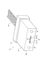
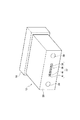
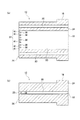
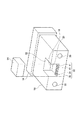
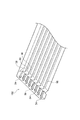
本発明の第1実施形態において、光コネクタの構成を示す斜視図である。In 1st Embodiment of this invention, it is a perspective view which shows the structure of an optical connector. 本発明の第1実施形態において、コネクタ本体の構成を示す斜視図である。In 1st Embodiment of this invention, it is a perspective view which shows the structure of a connector main body. 本発明の第1実施形態において、コネクタ本体の構成を示す断面図である。In 1st Embodiment of this invention, it is sectional drawing which shows the structure of a connector main body. 本発明の第1実施形態において、平面型光導波路の構成を示す斜視図である。1 is a perspective view showing a configuration of a planar optical waveguide in a first embodiment of the present invention. 本発明の第1実施形態において、他のコネクタ本体の構成を示す斜視図である。In 1st Embodiment of this invention, it is a perspective view which shows the structure of the other connector main body. 本発明の第1実施形態において、別なコネクタ本体の構成を示す斜視図である。In 1st Embodiment of this invention, it is a perspective view which shows the structure of another connector main body. 本発明の第1実施形態において、別なコネクタ本体の構成を示す斜視図である。In 1st Embodiment of this invention, it is a perspective view which shows the structure of another connector main body. 本発明の第1実施形態において、光コネクタの構成を示す斜視図である。In 1st Embodiment of this invention, it is a perspective view which shows the structure of an optical connector. 本発明の第2実施形態において、光コネクタの構成を示す斜視図である。In 2nd Embodiment of this invention, it is a perspective view which shows the structure of an optical connector. 本発明の第2実施形態において、コネクタ本体の構成を示す斜視図である。In 2nd Embodiment of this invention, it is a perspective view which shows the structure of a connector main body. 本発明の第2実施形態において、コネクタ本体の構成を示す断面図である。In 2nd Embodiment of this invention, it is sectional drawing which shows the structure of a connector main body. 本発明の第2実施形態において、平面型光導波路の構成を示す斜視図である。In 2nd Embodiment of this invention, it is a perspective view which shows the structure of a planar optical waveguide. 本発明の第3実施形態において、光コネクタの構成を示す斜視図である。In 3rd Embodiment of this invention, it is a perspective view which shows the structure of an optical connector. 本発明の第3実施形態において、光コネクタにおける要部の拡大図である。In 3rd Embodiment of this invention, it is an enlarged view of the principal part in an optical connector. 本発明の第3実施形態において、コネクタ本体の構成を示す断面図である。In 3rd Embodiment of this invention, it is sectional drawing which shows the structure of a connector main body. 本発明の第3実施形態において、光コネクタを光モジュールに取り付けた状態を示す光導波路挿通方向の断面図である。In 3rd Embodiment of this invention, it is sectional drawing of the optical waveguide penetration direction which shows the state which attached the optical connector to the optical module. 本発明の第4実施形態において、光コネクタの構成を示す斜視図である。In 4th Embodiment of this invention, it is a perspective view which shows the structure of an optical connector. 本発明の第4実施形態において、光コネクタにおける要部の拡大図である。In 4th Embodiment of this invention, it is an enlarged view of the principal part in an optical connector. 本発明の第4実施形態において、コネクタ本体の構成を示す断面図である。In 4th Embodiment of this invention, it is sectional drawing which shows the structure of a connector main body. 本発明の第5実施形態において、光コネクタの構成を示す斜視図である。In 5th Embodiment of this invention, it is a perspective view which shows the structure of an optical connector. 本発明の第5実施形態において、平面型光導波路の構成を示す斜視図である。In 5th Embodiment of this invention, it is a perspective view which shows the structure of a planar optical waveguide. 本発明の第5実施形態において、光コネクタにおける要部の断面斜視図である。In 5th Embodiment of this invention, it is a cross-sectional perspective view of the principal part in an optical connector. 本発明の第5実施形態において、光コネクタを光モジュールに取り付けた状態を示す光導波路挿通方向の断面図である。In 5th Embodiment of this invention, it is sectional drawing of the optical waveguide penetration direction which shows the state which attached the optical connector to the optical module. 本発明の第6実施形態において、光コネクタの構成を示す斜視図である。In 6th Embodiment of this invention, it is a perspective view which shows the structure of an optical connector. 本発明の第6実施形態において、平面型光導波路の構成を示す斜視図である。In 6th Embodiment of this invention, it is a perspective view which shows the structure of a planar optical waveguide. 本発明の第6実施形態において、光コネクタにおける要部の断面斜視図である。In 6th Embodiment of this invention, it is a cross-sectional perspective view of the principal part in an optical connector. 本発明の第7実施形態において、光コネクタの構成を示す斜視図である。In 7th Embodiment of this invention, it is a perspective view which shows the structure of an optical connector. 本発明の第7実施形態において、光コネクタの要部を示す拡大図である。In the 7th Embodiment of this invention, it is an enlarged view which shows the principal part of an optical connector. 本発明の第7実施形態において、光コネクタにおける平面型光導波路挿通方向の断面図である。In 7th Embodiment of this invention, it is sectional drawing of the planar optical waveguide penetration direction in an optical connector. 本発明の第8実施形態において、光コネクタの要部を示す拡大図である。In the 8th Embodiment of this invention, it is an enlarged view which shows the principal part of an optical connector. 本発明の第8実施形態において、平面型光導波路の構成を示す斜視図である。In the eighth embodiment of the present invention, it is a perspective view showing the configuration of a planar optical waveguide. 本発明の第8実施形態において、光コネクタにおける平面型光導波路挿通方向の断面図である。In 8th Embodiment of this invention, it is sectional drawing of the planar optical waveguide penetration direction in an optical connector.

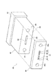
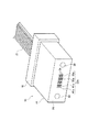
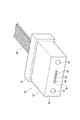
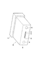
以下に図面を用いて本発明に係る第1実施形態について説明する。図1は、光コネクタ10の構成を示す斜視図である。光コネクタ10は、幅広で略角形に形成されたコネクタ本体12を備え、平面型光導波路14を保持する機能を有している。コネクタ本体12には、コネクタ本体12の後端側に設けられ、コネクタ本体12の外周面より外方へ突出して形成された鍔部16が設けられている。   A first embodiment according to the present invention will be described below with reference to the drawings. FIG. 1 is a perspective view showing the configuration of the optical connector 10. The optical connector 10 includes a connector body 12 that is wide and substantially rectangular, and has a function of holding a planar optical waveguide 14. The connector main body 12 is provided with a flange 16 that is provided on the rear end side of the connector main body 12 and protrudes outward from the outer peripheral surface of the connector main body 12.

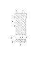
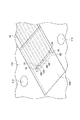
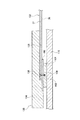
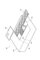
図2は、コネクタ本体12の構成を示す斜視図である。図3は、コネクタ本体12の構成を示す断面図であり、図3(a)は、コネクタ本体12における水平方向の断面図であり、図3(b)は、コネクタ本体における垂直方向の断面図である。図4は、平面型光導波路14の構成を示す斜視図である。   FIG. 2 is a perspective view showing the configuration of the connector body 12. 3 is a cross-sectional view showing the configuration of the connector main body 12, FIG. 3 (a) is a horizontal cross-sectional view of the connector main body 12, and FIG. 3 (b) is a vertical cross-sectional view of the connector main body. It is. FIG. 4 is a perspective view showing the configuration of the planar optical waveguide 14.

コネクタ本体12は、幅広で略角形に合成樹脂で金型成形等により成形される。コネクタ本体12は、例えば、エポキシ樹脂等の熱硬化性樹脂を用いたトランスファ成形や、ポリフェニレンサルファイド樹脂(PPS)や液晶ポリマ(LCP)等の熱可塑性樹脂を用いた射出成形等により成形される。   The connector body 12 is formed by molding or the like with a synthetic resin having a wide and substantially square shape. The connector body 12 is molded by, for example, transfer molding using a thermosetting resin such as an epoxy resin, injection molding using a thermoplastic resin such as polyphenylene sulfide resin (PPS) or liquid crystal polymer (LCP), or the like.

コネクタ本体12は、平面型光導波路14を挿入する光導波路挿入口18と、平面型光導波路14を挿通する光導波路挿通路20と、平面型光導波路14の先端を露出させる光導波路露出部22と、を有している。   The connector main body 12 includes an optical waveguide insertion port 18 into which the planar optical waveguide 14 is inserted, an optical waveguide insertion path 20 through which the planar optical waveguide 14 is inserted, and an optical waveguide exposed portion 22 that exposes the tip of the planar optical waveguide 14. And have.

光導波路挿入口18は、コネクタ本体後端面24に設けられ、平面型光導波路14をコネクタ本体12に挿入する機能を有している。光導波路挿入口18は、例えば、コネクタ本体後端面24の略中央に設けられ、平面型光導波路14を挿入可能な大きさで幅広の略矩形状に形成される。光導波路挿通路20は、コネクタ本体12に設けられ、光導波路挿入口18と連通し、平面型光導波路14を挿通する機能を有している。光導波路露出部22は、コネクタ本体前端面26に設けられ、光導波路挿通路20と連通し、平面型光導波路14の先端を露出させる機能を有している。光導波路露出部22は、例えば、平面型光導波路14の先端面と略同じ大きさで形成される。   The optical waveguide insertion port 18 is provided in the connector main body rear end surface 24 and has a function of inserting the planar optical waveguide 14 into the connector main body 12. The optical waveguide insertion port 18 is provided, for example, in the approximate center of the rear end surface 24 of the connector body, and is formed in a wide, substantially rectangular shape with a size that allows the planar optical waveguide 14 to be inserted. The optical waveguide insertion path 20 is provided in the connector main body 12, communicates with the optical waveguide insertion port 18, and has a function of inserting the planar optical waveguide 14. The optical waveguide exposure part 22 is provided on the front end face 26 of the connector body, communicates with the optical waveguide insertion path 20, and has a function of exposing the tip of the planar optical waveguide 14. The optical waveguide exposed portion 22 is formed with, for example, approximately the same size as the tip surface of the planar optical waveguide 14.

コネクタ本体12は、他の光コネクタとコネクタ接続等するときにコネクタ本体12を案内して位置決めするガイドピンが挿入される少なくとも1つのガイド穴30を有している。ガイド穴30は、例えば、コネクタ本体12に一対で設けられる。   The connector main body 12 has at least one guide hole 30 into which a guide pin for guiding and positioning the connector main body 12 when a connector is connected to another optical connector. For example, a pair of guide holes 30 are provided in the connector body 12.

平面型光導波路14は、図4に示すように、並列に1列に配列された複数のコア34と、複数のコア34を囲むクラッド36とを備え、例えば、略矩形状に形成される。平面型光導波路14には、マルチモード型の平面型光導波路、あるいはシングルモード型の平面型光導波路等を用いることができる。平面型光導波路14には、合成樹脂で形成されるフレキシブルな高分子製平面型光導波路や石英ガラスで形成される石英ガラス製平面型光導波路等が用いられる。高分子製平面型光導波路には、例えば、ポリイミド樹脂で形成された平面型光導波路が用いられる。   As shown in FIG. 4, the planar optical waveguide 14 includes a plurality of cores 34 arranged in a line in parallel and a clad 36 surrounding the plurality of cores 34, and is formed in a substantially rectangular shape, for example. The planar optical waveguide 14 may be a multimode planar optical waveguide, a single mode planar optical waveguide, or the like. As the planar optical waveguide 14, a flexible polymer planar optical waveguide formed of synthetic resin, a quartz glass planar optical waveguide formed of quartz glass, or the like is used. For example, a planar optical waveguide made of polyimide resin is used as the polymer planar optical waveguide.

コネクタ本体12は、光導波路露出部22に設けられ、光導波路挿通路20の通路底面から平面型光導波路14の挿通方向に対して略直交方向に突出して形成され、平面型光導波路14を嵌合してコネクタ本体12に位置決めする嵌合突起38を有している。また、平面型光導波路14は、平面型光導波路14の先端面に設けられ、平面型光導波路14のクラッド36に平面型光導波路14の光軸方向に対して略直交方向に溝状に形成され、嵌合突起38と嵌合される嵌合溝40を有している。   The connector main body 12 is provided in the optical waveguide exposed portion 22 and is formed so as to protrude in a direction substantially orthogonal to the insertion direction of the planar optical waveguide 14 from the bottom surface of the optical waveguide insertion path 20. And a fitting projection 38 for positioning on the connector body 12. The planar optical waveguide 14 is provided on the front end surface of the planar optical waveguide 14 and is formed in a groove shape in a direction substantially orthogonal to the optical axis direction of the planar optical waveguide 14 in the cladding 36 of the planar optical waveguide 14. And has a fitting groove 40 fitted to the fitting protrusion 38.

嵌合突起38は、例えば、光導波路挿通路20の通路底面から矩形状に突出した柱状の矩形突起で形成されることが好ましい。嵌合突起38は、例えば、平面型光導波路14の厚みと略同じ高さで形成され、平面型光導波路14における隣接するコア34とコア34との間の間隔より小さい幅で形成され、平面型光導波路14における嵌合溝40の溝深さと略同じ奥行で直方体状に形成される。   The fitting protrusion 38 is preferably formed of, for example, a columnar rectangular protrusion protruding in a rectangular shape from the bottom surface of the optical waveguide insertion path 20. The fitting projection 38 is formed, for example, at a height substantially the same as the thickness of the planar optical waveguide 14 and is formed with a width smaller than the interval between the adjacent cores 34 in the planar optical waveguide 14. The optical waveguide 14 is formed in a rectangular parallelepiped shape with a depth substantially the same as the depth of the fitting groove 40.

嵌合突起38は、光導波路露出部22に少なくとも1つ設けられる。また、嵌合突起38は、光導波路露出部22の一端から他端まで平面型光導波路14のコア列方向に沿って所定間隔で設けられることが好ましい。光導波路露出部22は、例えば、平面型光導波路14のコア列方向に1列に配列された複数の嵌合突起38により仕切られて、平面型光導波路14の各々コア34を露出させる複数のコア孔41が形成される。嵌合突起38は、例えば、コネクタ本体12に合成樹脂で一体成形されて設けられる。   At least one fitting protrusion 38 is provided on the optical waveguide exposed portion 22. The fitting protrusions 38 are preferably provided at predetermined intervals along the core row direction of the planar optical waveguide 14 from one end to the other end of the optical waveguide exposed portion 22. The optical waveguide exposed portion 22 is partitioned by, for example, a plurality of fitting protrusions 38 arranged in a row in the core row direction of the planar optical waveguide 14, and a plurality of cores 34 of the planar optical waveguide 14 are exposed. A core hole 41 is formed. The fitting protrusion 38 is provided, for example, by being integrally formed with the connector main body 12 with a synthetic resin.

平面型光導波路14は、図4に示すように、平面型光導波路14の先端面に設けられ、平面型光導波路14のクラッド36に平面型光導波路14の光軸方向に対して略直交方向に溝状に形成され、嵌合突起38と嵌合される嵌合溝40を有している。嵌合溝40は、平面型光導波路14における先端面のクラッド36に少なくとも1つ設けられる。嵌合溝40は、隣接するコア34とコア34との間のクラッド36に各々設けられ、平面型光導波路上面42から平面型光導波路下面44まで平面型光導波路14の厚み方向に貫通させた矩形溝で形成されることが好ましい。   As shown in FIG. 4, the planar optical waveguide 14 is provided on the distal end surface of the planar optical waveguide 14, and is approximately perpendicular to the optical axis direction of the planar optical waveguide 14 on the cladding 36 of the planar optical waveguide 14. And has a fitting groove 40 fitted to the fitting protrusion 38. At least one fitting groove 40 is provided in the cladding 36 on the distal end surface of the planar optical waveguide 14. The fitting grooves 40 are respectively provided in the clads 36 between the adjacent cores 34 and penetrated in the thickness direction of the planar optical waveguide 14 from the planar optical waveguide upper surface 42 to the planar optical waveguide lower surface 44. It is preferably formed by a rectangular groove.

嵌合溝40は、平面型光導波路14の隣接するコア34とコア34との間の間隔より狭い溝幅で形成され、平面型光導波路14の各々コア34に接触しないように設けられる。嵌合溝40は、嵌合突起38の奥行と略同じ溝深さで形成される。また、嵌合溝40の溝底面は、嵌合突起38と当接することにより平面型光導波路14の長手方向の位置を規制する位置規制面としての機能を有しており、嵌合溝40の溝側面は、嵌合突起38と当接することにより平面型光導波路14の幅方向の位置を規制する位置規制面としての機能を有している。嵌合溝40は、例えば、平面型光導波路14の先端面をダイジング加工またはレーザ加工等することにより形成される。   The fitting groove 40 is formed with a groove width narrower than the interval between the adjacent cores 34 of the planar optical waveguide 14 and is provided so as not to contact each core 34 of the planar optical waveguide 14. The fitting groove 40 is formed with substantially the same groove depth as the depth of the fitting protrusion 38. Further, the bottom surface of the fitting groove 40 has a function as a position regulating surface that regulates the position of the planar optical waveguide 14 in the longitudinal direction by contacting the fitting projection 38. The groove side surface functions as a position regulating surface that regulates the position of the planar optical waveguide 14 in the width direction by contacting the fitting protrusion 38. The fitting groove 40 is formed by, for example, dicing or laser processing the tip surface of the planar optical waveguide 14.

このように、嵌合突起38は、コネクタ本体12に凸状に設けられ、平面型光導波路14を嵌合してコネクタ本体12に位置決めする嵌合凸部としての機能を備えており、嵌合溝40は、平面型光導波路14に凹状に設けられ、嵌合凸部と嵌合される嵌合凹部としての機能を備えている。   Thus, the fitting protrusion 38 is provided in a convex shape on the connector main body 12 and has a function as a fitting convex portion for fitting the planar optical waveguide 14 and positioning it on the connector main body 12. The groove 40 is provided in a concave shape in the planar optical waveguide 14 and has a function as a fitting recess to be fitted with the fitting projection.

次に、コネクタ本体12に平面型光導波路14を装着して光コネクタ10を組み立てる組立方法について説明する。   Next, an assembly method for assembling the optical connector 10 by attaching the planar optical waveguide 14 to the connector body 12 will be described.

平面型光導波路14は、嵌合溝40が設けられた先端面をコネクタ本体12に向けて光導波路挿入口18から挿入され、先端面が光導波路露出部22に達するまで光導波路挿通路20で挿通される。そして、平面型光導波路14は、先端面の嵌合溝40を嵌合突起38に嵌合させることによりコネクタ本体12に位置決めされる。このため、平面型光導波路14の各々コア34は、光導波路露出部22のコア孔41から精度よく位置決めされて露出される。平面型光導波路14は、コネクタ本体12に位置決めされた後、接着剤等でコネクタ本体12に固着される。以上により、光コネクタ10の組み立てが完了する。   The planar optical waveguide 14 is inserted from the optical waveguide insertion port 18 with the front end surface provided with the fitting groove 40 facing the connector main body 12, and the optical waveguide insertion path 20 until the front end surface reaches the optical waveguide exposed portion 22. It is inserted. The planar optical waveguide 14 is positioned on the connector body 12 by fitting the fitting groove 40 on the distal end surface with the fitting protrusion 38. Therefore, each core 34 of the planar optical waveguide 14 is accurately positioned and exposed from the core hole 41 of the optical waveguide exposed portion 22. After the planar optical waveguide 14 is positioned on the connector body 12, it is fixed to the connector body 12 with an adhesive or the like. Thus, the assembly of the optical connector 10 is completed.

なお、コネクタ本体は、コネクタ本体前端面26の光導波路露出部22から開口され、光導波路挿通路20と連通し、平面型光導波路14の挿通方向に対して略直交方向に凹状に形成された凹部と、凹部を覆う蓋体とを備えるように構成されてもよい。図5は、他のコネクタ本体50の構成を示す斜視図である。なお、同様な要素には同一の符号を付し、詳細な説明を省略する。   The connector body is opened from the optical waveguide exposed portion 22 of the connector body front end face 26, communicates with the optical waveguide insertion path 20, and is formed in a concave shape in a direction substantially orthogonal to the insertion direction of the planar optical waveguide 14. You may comprise so that a recessed part and the cover body which covers a recessed part may be provided. FIG. 5 is a perspective view showing a configuration of another connector main body 50. In addition, the same code | symbol is attached | subjected to the same element and detailed description is abbreviate | omitted.

凹部52は、コネクタ本体50の光導波路露出部22から開口され、光導波路挿通路20と連通し、コネクタ本体50の上面から平面型光導波路14の挿通方向に対して略直交方向に凹状に形成される。コネクタ本体50に凹部52を設けることにより、平面型光導波路14の嵌合溝40がコネクタ本体50の嵌合突起38に嵌め込まれた状態を外観で確認できるので、平面型光導波路14におけるコア位置の位置精度をより向上させることができる。また、コネクタ本体50の凹部52から平面型光導波路14をコネクタ本体50に固着する接着剤を充填することができるので、接着剤の充填量を調節しながら平面型光導波路14を接着することができる。それにより、平面型光導波路14の固着後に行われる余分な接着剤を除去するための研磨工程等を省略できる。   The recess 52 is opened from the optical waveguide exposed portion 22 of the connector main body 50, communicates with the optical waveguide insertion path 20, and is formed in a concave shape in a direction substantially orthogonal to the insertion direction of the planar optical waveguide 14 from the upper surface of the connector main body 50. Is done. By providing the concave portion 52 in the connector main body 50, it is possible to confirm the appearance that the fitting groove 40 of the planar optical waveguide 14 is fitted into the fitting protrusion 38 of the connector main body 50, so that the core position in the planar optical waveguide 14 can be confirmed. The position accuracy can be further improved. In addition, since the adhesive for fixing the planar optical waveguide 14 to the connector body 50 can be filled from the recess 52 of the connector body 50, the planar optical waveguide 14 can be adhered while adjusting the filling amount of the adhesive. it can. Thereby, a polishing process or the like for removing excess adhesive performed after the planar optical waveguide 14 is fixed can be omitted.

蓋体54は、コネクタ本体50の凹部52に嵌合され、平面型光導波路14を覆って粉塵等から保護する機能を有している。蓋体54は、凹部52に挿入可能な大きさで成形され、例えば、エポキシ樹脂等の合成樹脂で矩形状に形成される。蓋体54は、蓋体下面を嵌合突起38の上端面に当接させて凹部52に嵌合される。   The lid 54 is fitted in the recess 52 of the connector body 50 and has a function of covering the planar optical waveguide 14 and protecting it from dust and the like. The lid 54 is formed in a size that can be inserted into the recess 52, and is formed in a rectangular shape with a synthetic resin such as an epoxy resin. The lid 54 is fitted into the recess 52 with the lower surface of the lid abutting against the upper end surface of the fitting projection 38.

また、コネクタ本体は、嵌合突起38が設けられた前端面側を別体として構成されてもよい。図6は、別なコネクタ本体60の構成を示す斜視図である。なお、同様な要素には同一の符号を付し、詳細な説明を省略する。   The connector main body may be configured with the front end surface provided with the fitting protrusion 38 as a separate body. FIG. 6 is a perspective view showing the configuration of another connector main body 60. In addition, the same code | symbol is attached | subjected to the same element and detailed description is abbreviate | omitted.

コネクタ本体60は、平面型光導波路14を保持する第1本体部62と、第1本体部62の前端面に取り付けられ、光導波路露出部22を含む第2本体部64と、を備えている。   The connector main body 60 includes a first main body portion 62 that holds the planar optical waveguide 14, and a second main body portion 64 that is attached to the front end surface of the first main body portion 62 and includes the optical waveguide exposed portion 22. .

第1本体部62は、第1本体部62の後端面に設けられる光導波路挿入口18と、光導波路挿入口18と連通する光導波路挿通路20と、を備えている。また、第1本体部62は、第1本体部62の前端面66に設けられ、光導波路挿通路20と連通し、平面型光導波路14の先端部を突出させる光導波路突出口68を有している。また、第1本体部62には、ガイドピンを挿入する一対のガイド穴30が設けられている。   The first main body 62 includes an optical waveguide insertion opening 18 provided on the rear end surface of the first main body 62 and an optical waveguide insertion passage 20 communicating with the optical waveguide insertion opening 18. The first main body portion 62 is provided on the front end surface 66 of the first main body portion 62, communicates with the optical waveguide insertion passage 20, and has an optical waveguide protrusion 68 that protrudes the tip portion of the planar optical waveguide 14. ing. Further, the first main body 62 is provided with a pair of guide holes 30 for inserting guide pins.

第2本体部64は、第1本体部62の前端面と当接して第1本体部62に取り付けられる。第2本体部64は、平面型光導波路14の先端部が挿入され、平面型光導波路14の先端を露出させる光導波路露出部22を備えている。光導波路露出部22には、平面型光導波路14のコア位置を位置決めする複数の嵌合突起38が設けられる。また、光導波路露出部22には、各嵌合突起38で仕切られて形成され、平面型光導波路14の各コアが露出される複数のコア孔41が設けられている。第2本体部64は、光導波路露出部22の両側にガイドピンが挿入される一対のガイド穴30aが設けられている。第1本体部62と第2本体部64とは、エポキシ樹脂等の同じ合成樹脂で形成されることが好ましい。   The second main body portion 64 is attached to the first main body portion 62 in contact with the front end surface of the first main body portion 62. The second main body portion 64 includes an optical waveguide exposing portion 22 into which the distal end portion of the planar optical waveguide 14 is inserted and the distal end of the planar optical waveguide 14 is exposed. The optical waveguide exposed portion 22 is provided with a plurality of fitting projections 38 for positioning the core position of the planar optical waveguide 14. Further, the optical waveguide exposed portion 22 is provided with a plurality of core holes 41 that are formed by being partitioned by the fitting protrusions 38 and from which the cores of the planar optical waveguide 14 are exposed. The second main body portion 64 is provided with a pair of guide holes 30 a into which guide pins are inserted on both sides of the optical waveguide exposed portion 22. The first main body 62 and the second main body 64 are preferably formed of the same synthetic resin such as an epoxy resin.

平面型光導波路14は、平面型光導波路14の先端部を光導波路突出口68から突出させて第1本体部62に取り付けられる。次に、平面型光導波路14の先端面に設けられた嵌合溝40に、第2本体部64の光導波路露出部22に設けられた嵌合突起38を嵌め込んで第2本体部64を第1本体部62に取り付ける。それにより、平面型光導波路14は、平面型光導波路14のコア位置の精度をより向上させてコネクタ本体60に装着される。嵌合突起38を有する第2本体部64を第1本体部62と別体で形成することにより、例えば、同じ形状の光導波路突出口68を有する外形形状の異なる第1本体部に対しても同一形状の第2本体部64を取り付けることができる。   The planar optical waveguide 14 is attached to the first main body 62 with the distal end of the planar optical waveguide 14 projecting from the optical waveguide projection 68. Next, the fitting protrusion 38 provided in the optical waveguide exposed portion 22 of the second main body portion 64 is fitted into the fitting groove 40 provided in the distal end surface of the planar optical waveguide 14 so that the second main body portion 64 is attached. It is attached to the first main body 62. Thereby, the planar optical waveguide 14 is mounted on the connector main body 60 with further improved accuracy of the core position of the planar optical waveguide 14. By forming the second main body portion 64 having the fitting protrusion 38 separately from the first main body portion 62, for example, for the first main body portion having the same shape and the optical waveguide protrusion 68 having a different outer shape. The second main body portion 64 having the same shape can be attached.

なお、第2本体部64を透明樹脂等の光学樹脂で形成し、光導波路露出部22に平面型光導波路14で伝送される信号光を集光する集光レンズや、PC(Physical Contact)用突起等の凸曲面突起を設けてもよい。図7は、光導波路露出部に凸曲面突起を設けた光コネクタ60aにおける垂直方向の断面図である。   The second main body 64 is formed of an optical resin such as a transparent resin, and a condensing lens that collects signal light transmitted through the planar optical waveguide 14 on the optical waveguide exposed portion 22 or for a PC (Physical Contact). Convex curved protrusions such as protrusions may be provided. FIG. 7 is a vertical cross-sectional view of an optical connector 60a in which convex curved protrusions are provided on the exposed portion of the optical waveguide.

光コネクタ60aは、エポキシ樹脂等で形成される第1本体部62と、光学樹脂で形成される第2本体部64aと、を備えている。第2本体部64aの光導波路露出部22には、光学樹脂で形成される凸曲面突起69が設けられる。凸曲面突起69は、第2本体部64aと一体で成形されることが好ましい。凸曲面突起69は、各嵌合突起38で仕切られて形成された各コア孔41に各々設けられる。光導波路露出部22に集光レンズを設ける場合には、凸曲面突起69は、例えば、凸レンズで形成され、平面型光導波路14で伝送される信号光を集光して凸曲面突起69から出射することができる。また、光導波路露出部22にPC用突起を設ける場合には、凸曲面突起69は、例えば、凸球面突起で形成され、凸曲面突起69を弾性変形させて他の平面型光導波路と直接接触させることにより信号光の反射を抑えて他の光コネクタと接続することができる。   The optical connector 60a includes a first main body portion 62 formed of an epoxy resin or the like, and a second main body portion 64a formed of an optical resin. A convex curved projection 69 made of optical resin is provided on the optical waveguide exposed portion 22 of the second main body portion 64a. The convex curved protrusion 69 is preferably formed integrally with the second main body portion 64a. The convex curved projection 69 is provided in each core hole 41 formed by being partitioned by each fitting projection 38. When a condensing lens is provided on the optical waveguide exposed portion 22, the convex curved projection 69 is formed by a convex lens, for example, and collects signal light transmitted through the planar optical waveguide 14 and emits it from the convex curved projection 69. can do. Further, when the PC waveguide projection is provided on the optical waveguide exposed portion 22, the convex curved projection 69 is formed by, for example, a convex spherical projection, and the convex curved projection 69 is elastically deformed to directly contact another planar optical waveguide. By doing so, it is possible to suppress the reflection of the signal light and connect to another optical connector.

また、光コネクタに装着される平面型光導波路には、2層等の複数層の平面型光導波路層を積層して構成される平面型光導波路積層体を用いてもよい。図8は、光コネクタ70の構成を示す斜視図である。光コネクタ70は、平面型光導波路積層体72をコネクタ本体74に装着して構成される。   Further, a planar optical waveguide laminate configured by laminating a plurality of planar optical waveguide layers such as two layers may be used for the planar optical waveguide attached to the optical connector. FIG. 8 is a perspective view showing the configuration of the optical connector 70. The optical connector 70 is configured by mounting a planar optical waveguide laminate 72 on a connector main body 74.

平面型光導波路積層体72は、例えば、図4に示される平面型光導波路14からなる平面型光導波路層を厚み方向に2層積層して構成される。平面型光導波路積層体72は、各平面型光導波路層の嵌合溝40が一致するようにして積層されて形成される。平面型光導波路積層体72の嵌合溝は、平面型光導波路積層体72の光軸方向に対して略直交方向に溝状に設けられ、平面型光導波路積層体上面から平面型光導波路積層体下面まで平面型光導波路積層体72の厚み方向に貫通させた矩形溝で形成される。   The planar optical waveguide laminate 72 is configured, for example, by laminating two planar optical waveguide layers composed of the planar optical waveguide 14 shown in FIG. 4 in the thickness direction. The planar optical waveguide laminate 72 is formed by laminating so that the fitting grooves 40 of the planar optical waveguide layers coincide with each other. The fitting groove of the planar optical waveguide laminate 72 is provided in a groove shape in a direction substantially orthogonal to the optical axis direction of the planar optical waveguide laminate 72, and the planar optical waveguide laminate is formed from the upper surface of the planar optical waveguide laminate. It is formed by a rectangular groove that penetrates in the thickness direction of the planar optical waveguide laminate 72 to the lower surface of the body.

コネクタ本体74は、コネクタ本体74の前端面に設けられ、平面型光導波路積層体72の先端面が露出可能な大きさで形成される光導波路露出部22aを有している。光導波路露出部22aは、平面型光導波路積層体72の嵌合溝と嵌合され、平面型光導波路積層体72をコネクタ本体74に位置決めする少なくとも1つの嵌合突起38aを有している。また、嵌合突起38aは、平面型光導波路積層体72のコア列方向に沿って隣接するコア34の間のクラッド36に各々設けられることが好ましい。嵌合突起38aは、平面型光導波路積層体72の厚みと略同じ高さで形成される。例えば、嵌合突起38aの高さは、図1に示す嵌合突起38の高さの略2倍で形成される。また、また、光導波路露出部22aには、各嵌合突起38aで仕切られて形成され、平面型光導波路積層体72の各コアが露出される少なくとも1つのコア孔41aが設けられている。   The connector main body 74 has an optical waveguide exposed portion 22a that is provided on the front end surface of the connector main body 74 and is formed to have a size that allows the front end surface of the planar optical waveguide laminate 72 to be exposed. The optical waveguide exposed portion 22 a has at least one fitting protrusion 38 a that is fitted into the fitting groove of the planar optical waveguide laminate 72 and positions the planar optical waveguide laminate 72 to the connector main body 74. The fitting protrusions 38 a are preferably provided on the clads 36 between the cores 34 adjacent to each other in the core row direction of the planar optical waveguide laminate 72. The fitting protrusion 38 a is formed with a height substantially the same as the thickness of the planar optical waveguide laminate 72. For example, the height of the fitting protrusion 38a is approximately twice the height of the fitting protrusion 38 shown in FIG. Further, the optical waveguide exposed portion 22a is provided with at least one core hole 41a formed by being partitioned by the fitting protrusions 38a and exposing each core of the planar optical waveguide laminate 72.

平面型光導波路積層体72は、平面型光導波路積層体72の嵌合溝をコネクタ本体74の嵌合突起38aに嵌合させることにより、平面型光導波路積層体72がコネクタ本体74に位置決めされる。それにより、平面型光導波路積層体72におけるコア位置の位置精度をより向上させた二次元配列型の光コネクタ70が組み立てられる。なお、上述した光コネクタ70では、2層に積層して構成された平面型光導波路積層体72について説明したが、平面型光導波路積層体72は、2層に限定されることなく、3層等の複数層で構成されてもよい。   The planar optical waveguide laminate 72 is positioned on the connector body 74 by fitting the fitting groove of the planar optical waveguide laminate 72 to the fitting projection 38 a of the connector body 74. The Thereby, the two-dimensional array type optical connector 70 in which the position accuracy of the core position in the planar optical waveguide laminate 72 is further improved is assembled. In the optical connector 70 described above, the planar optical waveguide laminate 72 formed by laminating two layers has been described. However, the planar optical waveguide laminate 72 is not limited to two layers, but has three layers. Etc. may be composed of a plurality of layers.

次に、本発明に係る第2実施形態について説明する。   Next, a second embodiment according to the present invention will be described.

図9は、光コネクタ80の構成を示す斜視図である。図10は、コネクタ本体82の構成を示す斜視図である。図11は、コネクタ本体82の構成を示す断面図であり、図11(a)は、コネクタ本体82における水平方向の断面図であり、図11(b)は、コネクタ本体82における垂直方向の断面図である。図12は、平面型光導波路84の構成を示す斜視図である。なお、同様な要素には同一の符号を付し、詳細な説明を省略する。   FIG. 9 is a perspective view showing the configuration of the optical connector 80. FIG. 10 is a perspective view showing the configuration of the connector main body 82. 11 is a cross-sectional view showing the configuration of the connector main body 82, FIG. 11 (a) is a horizontal cross-sectional view of the connector main body 82, and FIG. 11 (b) is a vertical cross-section of the connector main body 82. FIG. FIG. 12 is a perspective view showing the configuration of the planar optical waveguide 84. In addition, the same code | symbol is attached | subjected to the same element and detailed description is abbreviate | omitted.

光コネクタ80は、幅広で略角形にエポキシ樹脂等の合成樹脂で形成されるコネクタ本体82を備えている。コネクタ本体82は、コネクタ本体後端面86に設けられ、平面型光導波路84を挿入する光導波路挿入口18と、コネクタ本体82に設けられ、光導波路挿入口18と連通し、平面型光導波路84を挿通する光導波路挿通路20と、コネクタ本体前端面88に設けられ、光導波路挿通路20と連通し、平面型光導波路84の先端を露出させる光導波路露出口90と、を備えている。光導波路露出口90は、平面型光導波路84の先端面と略同じ大きさで形成される。   The optical connector 80 includes a connector body 82 that is wide and substantially square and formed of a synthetic resin such as an epoxy resin. The connector main body 82 is provided on the rear end face 86 of the connector main body, and is provided in the optical waveguide insertion slot 18 into which the flat optical waveguide 84 is inserted. The connector main body 82 is provided in the connector main body 82 and communicates with the optical waveguide insertion opening 18. And an optical waveguide exposure port 90 that is provided on the front end surface 88 of the connector main body, communicates with the optical waveguide insertion path 20, and exposes the tip of the planar optical waveguide 84. The optical waveguide exposure opening 90 is formed to have substantially the same size as the distal end surface of the planar optical waveguide 84.

コネクタ本体82は、他の光コネクタとコネクタ接続等するときにコネクタ本体82を案内して位置決めするガイドピンが挿入される少なくとも1つのガイド穴30を有している。ガイド穴30は、例えば、コネクタ本体82に一対で設けられる。   The connector main body 82 has at least one guide hole 30 into which a guide pin for guiding and positioning the connector main body 82 when a connector is connected to another optical connector or the like. For example, a pair of guide holes 30 are provided in the connector main body 82.

コネクタ本体82は、光導波路挿通路20の通路底面に設けられ、光導波路露出口90から平面型光導波路84の挿通方向に沿って突出して形成され、平面型光導波路84を嵌合してコネクタ本体82に位置決めする嵌合凸条92を有している。嵌合凸条92は、平面型光導波路84の挿通方向に対して略直交方向に突出して形成される。   The connector body 82 is provided on the bottom surface of the optical waveguide insertion path 20 and is formed to protrude from the optical waveguide exposure opening 90 along the insertion direction of the planar optical waveguide 84. The main body 82 has a fitting protrusion 92 for positioning. The fitting protrusion 92 is formed so as to protrude in a direction substantially orthogonal to the insertion direction of the planar optical waveguide 84.

嵌合凸条92は、平面型光導波路84の挿通方向に対して略直交方向の断面を略三角形状等の山型状に形成された突起である山型突起や、略円弧状のR型形状に形成された突起である円弧突起で形成されることが好ましい。勿論、嵌合凸条92は、山型突起や円弧突起等に限定されることはない。   The fitting ridge 92 is a ridge-shaped protrusion which is a protrusion formed in a ridge shape such as a substantially triangular shape in a section substantially perpendicular to the insertion direction of the planar optical waveguide 84, or a substantially arc-shaped R-shape. It is preferable to be formed by arcuate protrusions that are protrusions formed in a shape. Of course, the fitting ridge 92 is not limited to a chevron projection or an arc projection.

嵌合凸条92は、光導波路挿通路20の通路底面に少なくとも1つ設けられる。嵌合凸条92は、光導波路挿通路20における一方の通路側壁から他方の通路側壁まで所定間隔で複数設けられ、平面型光導波路84のコア列方向に沿って形成されることが好ましい。嵌合凸条92は、例えば、平面型光導波路84の厚みより小さい高さで形成され、平面型光導波路84における隣接するコア34とコア34との間隔よりも小さい幅で形成される。嵌合凸条92は、例えば、コネクタ本体82に合成樹脂で一体成形されて設けられる。   At least one fitting protrusion 92 is provided on the bottom surface of the optical waveguide insertion path 20. It is preferable that a plurality of fitting protrusions 92 are provided at a predetermined interval from one passage side wall to the other passage side wall in the optical waveguide insertion path 20 and are formed along the core row direction of the planar optical waveguide 84. The fitting protrusion 92 is formed with a height smaller than the thickness of the planar optical waveguide 84, for example, and is formed with a width smaller than the interval between the adjacent cores 34 in the planar optical waveguide 84. The fitting protrusions 92 are provided, for example, by being integrally formed with the connector main body 82 with a synthetic resin.

平面型光導波路84は、平面型光導波路84のクラッド36に先端面から光軸方向に沿って溝状に形成され、嵌合凸条92と嵌合される嵌合凹条96を有している。嵌合凹条96は、平面型光導波路下面94に平面型光導波路84の先端面から平面型光導波路84の光軸方向に沿って所定長さで少なくとも1つ設けられる。また、嵌合凹条96は、隣接するコア34とコア34との間のクラッド36に平面型光導波路84の先端面から平面型光導波路84の光軸方向に沿って所定長さで各々形成されることが好ましい。嵌合凹条96における長手方向の長さは、嵌合凸条92の長手方向の長さと略同じであることが好ましい。   The planar optical waveguide 84 has a fitting groove 96 that is formed in a groove shape along the optical axis direction from the front end surface of the clad 36 of the planar optical waveguide 84 and is fitted to the fitting protrusion 92. Yes. At least one fitting groove 96 is provided on the lower surface 94 of the planar optical waveguide with a predetermined length from the front end surface of the planar optical waveguide 84 along the optical axis direction of the planar optical waveguide 84. The fitting recesses 96 are respectively formed in the cladding 36 between the adjacent cores 34 with a predetermined length from the front end surface of the planar optical waveguide 84 along the optical axis direction of the planar optical waveguide 84. It is preferred that The length in the longitudinal direction of the fitting concave strip 96 is preferably substantially the same as the length in the longitudinal direction of the fitting convex strip 92.

嵌合凹条96は、平面型光導波路84の光軸方向に対して略直交方向の断面を、略三角形状したV溝や、略円弧状にした円弧溝で形成されることが好ましい。例えば、コネクタ本体82の嵌合凸条92が山型突起で形成される場合には、平面型光導波路84の嵌合凹条96はV溝で形成され、コネクタ本体82の嵌合凸条92が円弧突起で形成される場合には、平面型光導波路84の嵌合凹条96は円弧溝で形成される。勿論、嵌合凹条96は、V溝や円弧溝等に限定されることはない。また、嵌合凹条96の内周面は、嵌合凸条92と当接することにより平面型光導波路84の幅方向の位置を規制する位置規制面としての機能を有している。   The fitting recess 96 is preferably formed by a substantially triangular V-shaped groove or an arc-shaped groove having a substantially orthogonal cross section in the direction perpendicular to the optical axis direction of the planar optical waveguide 84. For example, when the fitting ridge 92 of the connector main body 82 is formed with an angled projection, the fitting ridge 96 of the planar optical waveguide 84 is formed with a V-groove, and the fitting ridge 92 of the connector main body 82 is formed. Is formed by an arc-shaped protrusion, the fitting recess 96 of the planar optical waveguide 84 is formed by an arc-shaped groove. Of course, the fitting groove 96 is not limited to a V-groove, a circular arc groove or the like. Further, the inner peripheral surface of the fitting recess 96 has a function as a position restricting surface that restricts the position of the planar optical waveguide 84 in the width direction by contacting the fitting protrusion 92.

平面型光導波路84は、平面型光導波路下面94に設けられた嵌合凹条96をコネクタ本体82の嵌合凸条92に嵌合させてコネクタ本体82に位置決めされる。それにより、平面型光導波路84におけるコア位置の位置精度をより向上させることができる。このように、嵌合凸条92は、コネクタ本体82に凸状に設けられ、平面型光導波路84を嵌合してコネクタ本体82に位置決めする嵌合凸部としての機能を備えており、嵌合凹条96は、平面型光導波路84に凹状に設けられ、嵌合凸部と嵌合される嵌合凹部としての機能を備えている。   The planar optical waveguide 84 is positioned on the connector main body 82 by fitting a fitting concave 96 provided on the lower surface 94 of the planar optical waveguide to the fitting convex 92 of the connector main body 82. Thereby, the position accuracy of the core position in the planar optical waveguide 84 can be further improved. Thus, the fitting protrusion 92 is provided in a convex shape on the connector body 82, and has a function as a fitting protrusion for fitting the planar optical waveguide 84 and positioning it on the connector body 82. The joint recess 96 is provided in a concave shape in the planar optical waveguide 84 and has a function as a fitting recess to be fitted with the fitting projection.

次に、本発明に係る第3実施形態について説明する。   Next, a third embodiment according to the present invention will be described.

図13は、光コネクタ100の構成を示す斜視図である。図14は、光コネクタ100における要部の拡大図である。図15は、光コネクタ100における平面型光導波路挿通方向の断面図である。図16は、光コネクタ100を光モジュール101に取り付けた状態を示す平面型光導波路挿通方向の断面図である。なお、同様な要素には同一の符号を付し、詳細な説明を省略する。   FIG. 13 is a perspective view showing the configuration of the optical connector 100. FIG. 14 is an enlarged view of a main part of the optical connector 100. FIG. 15 is a cross-sectional view of the optical connector 100 in the planar optical waveguide insertion direction. FIG. 16 is a cross-sectional view of the planar optical waveguide insertion direction showing a state in which the optical connector 100 is attached to the optical module 101. In addition, the same code | symbol is attached | subjected to the same element and detailed description is abbreviate | omitted.

光コネクタ100は、光素子部品としての機能を有する光モジュール101の光素子102に対向して配置され、平面型光導波路14と光素子102との間を光結合する機能を有している。光素子102は、発光素子または受光素子で構成され、光モジュール101の光入出力端としての機能を有している。発光素子には、面発光素子型レーザダイオード(VCSEL:Vertical Cavity Surface−Emitting Laser)等が用いられ、受光素子には、フォトダイオード(PD:Photo Diode)等が用いられる。   The optical connector 100 is disposed to face the optical element 102 of the optical module 101 having a function as an optical element component, and has a function of optically coupling between the planar optical waveguide 14 and the optical element 102. The optical element 102 includes a light emitting element or a light receiving element, and has a function as an optical input / output end of the optical module 101. A surface emitting element type laser diode (VCSEL) is used as the light emitting element, and a photodiode (PD: Photo Diode) is used as the light receiving element.

光コネクタ100は、幅広で略角形にエポキシ樹脂等の合成樹脂で形成されるコネクタ本体103を備えている。コネクタ本体103は、コネクタ本体103の後端面から略中央まで溝状に設けられ、平面型光導波路14を挿通する光導波路挿通溝104と、光導波路挿通溝104の前溝壁に設けられ、平面型光導波路14の光軸方向の延長上に対して傾斜して形成され、平面型光導波路14を伝搬する信号光の光軸方向を反射により変更させる光路変更面106と、を備えている。   The optical connector 100 includes a connector body 103 that is wide and is substantially square and formed of a synthetic resin such as an epoxy resin. The connector main body 103 is provided in a groove shape from the rear end surface of the connector main body 103 to a substantially center, and is provided in the optical waveguide insertion groove 104 for inserting the planar optical waveguide 14 and the front groove wall of the optical waveguide insertion groove 104. And an optical path changing surface 106 which is formed to be inclined with respect to the extension of the optical waveguide 14 in the optical axis direction and changes the optical axis direction of the signal light propagating through the planar optical waveguide 14 by reflection.

光導波路挿通溝104は、平面型光導波路14を挿通して配置可能に設けられ、平面型光導波路14の幅より大きい溝幅で形成され、平面型光導波路14の厚みより深い溝深さで形成される。光導波路挿通溝104の溝周縁には、後述するシート状の透光部材108を当接して取り付ける透光部材取付部110が設けられる。   The optical waveguide insertion groove 104 is provided so as to be inserted through the planar optical waveguide 14, is formed with a groove width larger than the width of the planar optical waveguide 14, and has a groove depth deeper than the thickness of the planar optical waveguide 14. It is formed. A translucent member attaching portion 110 that attaches a sheet-like translucent member 108 to be described later in contact is provided on the periphery of the optical waveguide insertion groove 104.

光路変更面106は、光導波路挿通溝104の前溝壁に光素子102と対向するように設けられ、平面型光導波路14の先端面と対向して平面型光導波路14の光軸方向の延長上に傾斜して形成され、平面型光導波路14を伝搬する信号光の光軸方向を反射により変更させて平面型光導波路14と光素子102との間を光結合させる機能を有している。光路変更面106は、例えば、光導波路挿通溝104の溝底面からコネクタ本体103の前端面側に広がるように傾斜させて形成される。光路変更面106は、例えば、傾斜面に金属蒸着等した反射ミラーで構成される。   The optical path changing surface 106 is provided on the front groove wall of the optical waveguide insertion groove 104 so as to face the optical element 102, and is opposed to the distal end surface of the planar optical waveguide 14 to extend in the optical axis direction of the planar optical waveguide 14. It is inclined upward and has a function of optically coupling between the planar optical waveguide 14 and the optical element 102 by changing the optical axis direction of the signal light propagating through the planar optical waveguide 14 by reflection. . For example, the optical path changing surface 106 is formed to be inclined so as to spread from the groove bottom surface of the optical waveguide insertion groove 104 to the front end surface side of the connector main body 103. The optical path changing surface 106 is constituted by, for example, a reflection mirror that is formed by metal vapor deposition on an inclined surface.

光路変更面106は、平面型光導波路14の光軸方向に対して略45度傾斜して形成されることが好ましい。それにより、光コネクタ100を光モジュール101に設置したときに、光モジュール101に設けられた光素子102の上方に位置して光素子102の発光面または受光面と対面し、平面型光導波路14の先端面から出射された信号光を略90度に屈曲させて光素子102に入射させることができ、光素子102から出射された信号光を略90度に屈曲させて平面型光導波路14に入射させることができる。   The optical path changing surface 106 is preferably formed with an inclination of approximately 45 degrees with respect to the optical axis direction of the planar optical waveguide 14. Accordingly, when the optical connector 100 is installed in the optical module 101, the optical connector 100 is positioned above the optical element 102 provided in the optical module 101 so as to face the light emitting surface or the light receiving surface of the optical element 102. The signal light emitted from the front end surface of the optical element 102 can be bent by approximately 90 degrees and incident on the optical element 102, and the signal light emitted from the optical element 102 can be bent by approximately 90 degrees to form the planar optical waveguide 14. It can be made incident.

光路変更面106の傾斜角度は、平面型光導波路14の光軸方向に対して略45度の傾斜角が好ましいが、必ずしも略45度に限定されることはない。光路変更面106は、平面型光導波路14の先端面から出射された信号光が光素子102に入射するような反射が可能であり、光素子102から出射された信号光が平面型光導波路14に入射するような反射が可能である傾斜角度で形成される。   The tilt angle of the optical path changing surface 106 is preferably approximately 45 degrees with respect to the optical axis direction of the planar optical waveguide 14, but is not necessarily limited to approximately 45 degrees. The optical path changing surface 106 can reflect such that the signal light emitted from the distal end surface of the planar optical waveguide 14 enters the optical element 102, and the signal light emitted from the optical element 102 can be reflected by the planar optical waveguide 14. It is formed at an inclination angle that allows reflection to be incident on the light.

光路変更面106は、平面型光導波路14から出射された信号光を集光する凹鏡面を有していることが好ましい。凹鏡面は、平面型光導波路14の光軸方向の延長上に形成され、平面型光導波路14から出射された信号光を光素子102に正しく焦点を結ぶように集光し、光素子102から出射された信号光を平面型光導波路14の先端面に正しく焦点を結ぶように信号光を集光させることができる。信号光を集光させることにより信号光の拡散を抑制できるので、平面型光導波路14と光素子102との間の光結合効率を向上させることができる。凹鏡面は、例えば、球面、あるいは回転放物線面(パラボラ面)等の非球面で形成される。凹鏡面は、平面型光導波路14のコア34ごとに光路変更面106に複数個設けられることが好ましい。   The optical path changing surface 106 preferably has a concave mirror surface that collects the signal light emitted from the planar optical waveguide 14. The concave mirror surface is formed on the extension of the planar optical waveguide 14 in the optical axis direction, condenses the signal light emitted from the planar optical waveguide 14 so as to be correctly focused on the optical element 102, and from the optical element 102. The signal light can be condensed so that the emitted signal light is correctly focused on the distal end surface of the planar optical waveguide 14. Since the diffusion of the signal light can be suppressed by condensing the signal light, the optical coupling efficiency between the planar optical waveguide 14 and the optical element 102 can be improved. The concave mirror surface is formed of an aspherical surface such as a spherical surface or a parabolic surface (parabolic surface), for example. A plurality of concave mirror surfaces are preferably provided on the optical path changing surface 106 for each core 34 of the planar optical waveguide 14.

透光部材108は、光学樹脂や光学ガラス等でシート状に形成され、光路変更面106を覆い、透光部材取付部110に取り付けられる。透光部材108は、使用される信号波長(例えば、850nm、1310nm、1550nm等)の光を効率よく透過する光学樹脂で形成されることが好ましい。光学樹脂には、PC(ポリカーボネイト樹脂)、PEI(ポリエーテルイミド樹脂)、PPA(ポリフタルアミド樹脂)等を用いることができる。平面型光導波路14の先端面から出射され、光路変更面106で反射された信号光は、透光部材108を透過して光素子102に入射される。また、光素子102から出射された信号光は、透光部材108を透過して光路変更面106で反射され平面型光導波路14の先端面に入射される。   The translucent member 108 is formed into a sheet shape with optical resin, optical glass, or the like, covers the optical path changing surface 106, and is attached to the translucent member attaching portion 110. The translucent member 108 is preferably formed of an optical resin that efficiently transmits light having a signal wavelength to be used (for example, 850 nm, 1310 nm, 1550 nm, etc.). As the optical resin, PC (polycarbonate resin), PEI (polyetherimide resin), PPA (polyphthalamide resin), or the like can be used. The signal light emitted from the front end surface of the planar optical waveguide 14 and reflected by the optical path changing surface 106 passes through the light transmitting member 108 and enters the optical element 102. The signal light emitted from the optical element 102 passes through the light transmitting member 108, is reflected by the optical path changing surface 106, and enters the front end surface of the planar optical waveguide 14.

透光部材108に信号光が入出射する透光部材光入出射面109には、信号光の信号波長より小さい周期で凹凸状に配列されて形成された凹凸部が設けられることが好ましい。周知のように透光部材光入出射面109に信号光の信号波長より小さい周期で凹凸状に配列された微細な凹凸部を形成することにより、透光部材光入出射面109での信号光の反射を無反射状態にすることができる。微細凹凸部は、例えば、精密な金型を用いて透光部材光入出射面109に直接形成することができる。   The translucent member light incident / exit surface 109 through which signal light enters and exits the translucent member 108 is preferably provided with concave and convex portions that are arranged in an irregular manner with a period smaller than the signal wavelength of the signal light. As is well known, by forming fine uneven portions arranged in an uneven shape with a period smaller than the signal wavelength of the signal light on the light transmitting member light incident / exit surface 109, the signal light on the light transmitting member light incident / exit surface 109 is formed. Can be made non-reflective. The fine uneven portion can be directly formed on the light incident / exit surface 109 of the translucent member using, for example, a precise mold.

また、反射防止膜を透光部材光入出射面109に設けることにより、透光部材光入出射面109での信号光の反射を防止してもよい。反射防止膜は、例えば、誘電体材料を透光部材光入出射面109に塗布、真空蒸着またはスパッタリング等することにより形成される。更に、光減衰膜を透光部材光入出射面109に設けることにより、信号光の光強度を低下させることができるので目の安全性をより向上させることができる。光減衰膜は、例えば、金属材料等をスパッタリングして形成される。   Further, by providing an antireflection film on the light transmissive member light incident / exit surface 109, reflection of signal light on the light transmissive member light incident / exit surface 109 may be prevented. The antireflection film is formed, for example, by applying a dielectric material to the light incident / exiting surface 109 of the translucent member, vacuum deposition or sputtering. Furthermore, by providing the light attenuating film on the light incident / exiting surface 109 of the translucent member, the light intensity of the signal light can be lowered, and thus the safety of the eyes can be further improved. The light attenuation film is formed, for example, by sputtering a metal material or the like.

コネクタ本体103は、コネクタ本体103を光モジュール101に位置決めするガイドピンが挿入される少なくとも1つのガイド穴112を有している。例えば、光モジュール101に突出させて設けられたガイドピンをガイド穴112に挿入してコネクタ本体103を取り付けることにより、コネクタ本体103を光モジュール101の光素子102に精度よく対向させて位置決めできる。ガイド穴112は、例えば、光導波路挿通溝104を挟んで光路変更面106の近傍に一対で設けられる。光コネクタ100は、ガイドピンで案内されて、光路変更面106が光モジュール101の光素子102に対面して位置するように光モジュール101に取り付けられる。なお、光モジュール101にコネクタ本体103を位置決めするガイド穴を設け、コネクタ本体103に光モジュール101のガイド穴に挿入されるガイドピンを設けてもよい。   The connector main body 103 has at least one guide hole 112 into which a guide pin for positioning the connector main body 103 to the optical module 101 is inserted. For example, by inserting a guide pin provided protruding from the optical module 101 into the guide hole 112 and attaching the connector main body 103, the connector main body 103 can be positioned accurately facing the optical element 102 of the optical module 101. For example, a pair of guide holes 112 are provided in the vicinity of the optical path changing surface 106 with the optical waveguide insertion groove 104 interposed therebetween. The optical connector 100 is guided by a guide pin, and is attached to the optical module 101 so that the optical path changing surface 106 faces the optical element 102 of the optical module 101. The optical module 101 may be provided with a guide hole for positioning the connector main body 103, and the connector main body 103 may be provided with a guide pin inserted into the guide hole of the optical module 101.

コネクタ本体103は、光導波路挿通溝104の溝底面に光路変更面106と対向して設けられ、光導波路挿通溝104の溝底面から平面型光導波路14の挿通方向に対して略直交方向に突出して形成され、平面型光導波路14を嵌合してコネクタ本体103に位置決めする嵌合突起114を有している。また、平面型光導波路14は、平面型光導波路14の先端面に設けられ、平面型光導波路14のクラッド36に平面型光導波路14の光軸方向に対して略直交方向に溝状に形成され、嵌合突起114と嵌合される嵌合溝40を有している。平面型光導波路14には、上述した第1実施形態の光コネクタ10に用いられる平面型光導波路と同じものが用いられる。   The connector body 103 is provided on the groove bottom surface of the optical waveguide insertion groove 104 so as to face the optical path changing surface 106, and protrudes from the groove bottom surface of the optical waveguide insertion groove 104 in a direction substantially orthogonal to the insertion direction of the planar optical waveguide 14. And has a fitting projection 114 for fitting the planar optical waveguide 14 to the connector main body 103 for positioning. The planar optical waveguide 14 is provided on the front end surface of the planar optical waveguide 14 and is formed in a groove shape in a direction substantially orthogonal to the optical axis direction of the planar optical waveguide 14 in the cladding 36 of the planar optical waveguide 14. And has a fitting groove 40 fitted to the fitting protrusion 114. The planar optical waveguide 14 is the same as the planar optical waveguide used in the optical connector 10 of the first embodiment described above.

嵌合突起114は、光路変更面106の近傍に設けられることが好ましく、光路変更面106の縁に設けられることがより好ましい。嵌合突起114は、嵌合突起38と同様の形状で形成され、例えば、矩形状に突出した矩形突起で形成される。嵌合突起114は、光導波路挿通溝104に少なくとも1つ設けられる。また、嵌合突起114は、光導波路挿通溝104における一方の溝側壁から他方の溝側壁まで所定間隔で複数設けられ、平面型光導波路14のコア列方向に沿って柱状に形成されることが好ましい。嵌合突起114は、例えば、コネクタ本体103に合成樹脂で一体成形されて設けられる。   The fitting protrusion 114 is preferably provided in the vicinity of the optical path changing surface 106, and more preferably provided on the edge of the optical path changing surface 106. The fitting protrusion 114 is formed in the same shape as the fitting protrusion 38, and is formed by, for example, a rectangular protrusion protruding in a rectangular shape. At least one fitting protrusion 114 is provided in the optical waveguide insertion groove 104. The plurality of fitting protrusions 114 are provided at a predetermined interval from one groove side wall to the other groove side wall in the optical waveguide insertion groove 104 and may be formed in a columnar shape along the core row direction of the planar optical waveguide 14. preferable. The fitting protrusion 114 is provided, for example, by being integrally formed with the connector main body 103 with a synthetic resin.

平面型光導波路14は、上述した図4に示すように、嵌合突起114と嵌合される嵌合溝40を有している。嵌合溝40は、平面型光導波路14における先端面のクラッド36に少なくとも1つ設けられる。嵌合溝40は、隣接するコア34とコア34との間のクラッド36に各々設けられ、平面型光導波路上面42から平面型光導波路下面44まで平面型光導波路14の厚み方向に貫通させた矩形溝で形成されることが好ましい。また、嵌合溝40の溝底面は、嵌合突起114と当接することにより平面型光導波路14の長手方向の位置を規制する位置規制面としての機能を有しており、嵌合溝40の溝側面は、嵌合突起114と当接することにより平面型光導波路14の幅方向の位置を規制する位置規制面としての機能を有している。   As shown in FIG. 4 described above, the planar optical waveguide 14 has a fitting groove 40 fitted to the fitting protrusion 114. At least one fitting groove 40 is provided in the cladding 36 on the distal end surface of the planar optical waveguide 14. The fitting grooves 40 are respectively provided in the clads 36 between the adjacent cores 34 and penetrated in the thickness direction of the planar optical waveguide 14 from the planar optical waveguide upper surface 42 to the planar optical waveguide lower surface 44. It is preferably formed by a rectangular groove. Further, the bottom surface of the fitting groove 40 has a function as a position regulating surface that regulates the position in the longitudinal direction of the planar optical waveguide 14 by contacting the fitting projection 114. The groove side surface functions as a position regulating surface that regulates the position of the planar optical waveguide 14 in the width direction by contacting the fitting protrusion 114.

平面型光導波路14は、先端面の嵌合溝40を嵌合突起114に嵌合させて光導波路挿通溝104に配置される。それにより、平面型光導波路14は、コア位置の位置精度をより向上させてコネクタ本体103に装着される。このように、嵌合突起114は、コネクタ本体103に凸状に設けられ、平面型光導波路14を嵌合してコネクタ本体103に位置決めする嵌合凸部としての機能を備えており、嵌合溝40は、平面型光導波路14に凹状に設けられ、嵌合凸部と嵌合される嵌合凹部としての機能を備えている。   The planar optical waveguide 14 is disposed in the optical waveguide insertion groove 104 by fitting the fitting groove 40 on the distal end surface with the fitting protrusion 114. Thereby, the planar optical waveguide 14 is attached to the connector main body 103 with further improved accuracy of the core position. Thus, the fitting protrusion 114 is provided in a convex shape on the connector main body 103 and has a function as a fitting convex portion for fitting the planar optical waveguide 14 and positioning it on the connector main body 103. The groove 40 is provided in a concave shape in the planar optical waveguide 14 and has a function as a fitting recess to be fitted with the fitting projection.

次に、光コネクタ100の作用について説明する。   Next, the operation of the optical connector 100 will be described.

光コネクタ100は、図16に示すように、回路基板115に配置された光モジュール101の光素子102に対向して配置され、光路変更面106側を光モジュール101に向けて取り付けられ、平面型光導波路14と光素子102との間を光結合する。光コネクタ100は、コネクタ本体103のガイド穴112に光モジュール101に設けられたガイドピンを挿通して、光モジュール101に位置決めされる。光コネクタ100は、ガイドピンで案内されて、光路変更面106が光素子102の光軸方向の延長上に位置決めされる。   As shown in FIG. 16, the optical connector 100 is disposed so as to face the optical element 102 of the optical module 101 disposed on the circuit board 115, and is attached with the optical path changing surface 106 side facing the optical module 101. Optical coupling between the optical waveguide 14 and the optical element 102 is performed. The optical connector 100 is positioned by the optical module 101 by inserting guide pins provided in the optical module 101 into the guide holes 112 of the connector main body 103. The optical connector 100 is guided by guide pins, and the optical path changing surface 106 is positioned on the extension of the optical element 102 in the optical axis direction.

光素子102が受光素子である場合には、平面型光導波路14で伝送された信号光は、光路変更面106で反射により略90度に屈曲させて光モジュール101の光素子102に入射される。また、光素子102が発光素子である場合には、光モジュール101の光素子102から出射された信号光は、光路変更面106で反射により略90度に屈曲されて平面型光導波路14の光軸方向に向けられ、平面型光導波路14の先端面に入射される。このようにして、光コネクタ100により、平面型光導波路14と光素子102との間が光結合される。   When the optical element 102 is a light receiving element, the signal light transmitted through the planar optical waveguide 14 is reflected by the optical path changing surface 106 by being bent at approximately 90 degrees and is incident on the optical element 102 of the optical module 101. . Further, when the optical element 102 is a light emitting element, the signal light emitted from the optical element 102 of the optical module 101 is bent at approximately 90 degrees by reflection at the optical path changing surface 106 and is emitted from the planar optical waveguide 14. It is directed in the axial direction and is incident on the tip surface of the planar optical waveguide 14. In this way, the optical connector 100 optically couples the planar optical waveguide 14 and the optical element 102.

次に、本発明の第4実施形態について説明する。   Next, a fourth embodiment of the present invention will be described.

図17は、光コネクタ120の構成を示す斜視図である。図18は、光コネクタ120における要部の拡大図である。図19は、光コネクタ120における光導波路挿通方向の断面図である。なお、同様な要素には同一の符号を付し、詳細な説明を省略する。   FIG. 17 is a perspective view showing the configuration of the optical connector 120. FIG. 18 is an enlarged view of a main part of the optical connector 120. FIG. 19 is a cross-sectional view of the optical connector 120 in the optical waveguide insertion direction. In addition, the same code | symbol is attached | subjected to the same element and detailed description is abbreviate | omitted.

光コネクタ120は、光モジュール101の光素子102に対向して配置され、平面型光導波路84と光素子102との間を光結合する機能を有している。なお、光コネクタ120は、図16に示される第3実施形態の光コネクタ100と同様にして光モジュール101に取り付けられる。   The optical connector 120 is disposed so as to face the optical element 102 of the optical module 101, and has a function of optically coupling between the planar optical waveguide 84 and the optical element 102. The optical connector 120 is attached to the optical module 101 in the same manner as the optical connector 100 of the third embodiment shown in FIG.

光コネクタ120は、幅広で略角形にエポキシ樹脂等の合成樹脂で形成されるコネクタ本体122を備えている。コネクタ本体122は、コネクタ本体122の後端面から略中央まで溝状に設けられ、平面型光導波路84を挿通して配置する光導波路挿通溝104と、光導波路挿通溝104の前溝壁に光素子102と対向するように設けられ、平面型光導波路84の光軸方向の延長上に対して傾斜して形成され、平面型光導波路84を伝搬する信号光の光軸方向を反射により変更させて平面型光導波路84と光素子102との間を光結合させる光路変更面106と、を備えている。   The optical connector 120 includes a connector body 122 that is wide and is substantially square and formed of a synthetic resin such as an epoxy resin. The connector main body 122 is provided in a groove shape from the rear end surface of the connector main body 122 to a substantially central position, and the optical waveguide insertion groove 104 that is inserted through the planar optical waveguide 84 is disposed on the front groove wall of the optical waveguide insertion groove 104. It is provided so as to face the element 102, is formed to be inclined with respect to the extension in the optical axis direction of the planar optical waveguide 84, and changes the optical axis direction of the signal light propagating through the planar optical waveguide 84 by reflection. The optical path changing surface 106 for optically coupling the planar optical waveguide 84 and the optical element 102 is provided.

光導波路挿通溝104の溝周縁には、シート状の透光部材108を当接して取り付ける透光部材取付部110が設けられている。また、コネクタ本体122は、光コネクタ120を光モジュール101に位置決めするガイドピンが挿通される一対のガイド穴112を有している。   On the periphery of the optical waveguide insertion groove 104, there is provided a translucent member attaching portion 110 that abuts and attaches the sheet-like translucent member 108. The connector body 122 has a pair of guide holes 112 through which guide pins for positioning the optical connector 120 to the optical module 101 are inserted.

コネクタ本体122は、光導波路挿通溝104の溝底面に設けられ、光路変更面106の面縁から平面型光導波路84の挿通方向に沿って突出して設けられ、平面型光導波路84を嵌合してコネクタ本体122に位置決めする嵌合凸条124を有している。また、平面型光導波路84は、クラッド36に平面型光導波路84の先端面から光軸方向に沿って溝状に形成され、嵌合凸条124と嵌合される嵌合凹条96を有している。平面型光導波路84には、上述した第2実施形態の光コネクタ80に用いられる平面型光導波路と同じものが用いられる。   The connector main body 122 is provided on the bottom surface of the optical waveguide insertion groove 104 and is provided so as to protrude from the surface edge of the optical path changing surface 106 along the insertion direction of the planar optical waveguide 84, and engages with the planar optical waveguide 84. And a fitting protrusion 124 for positioning the connector main body 122. Further, the planar optical waveguide 84 is formed in the clad 36 in the shape of a groove along the optical axis direction from the front end surface of the planar optical waveguide 84, and has a fitting groove 96 fitted to the fitting protrusion 124. doing. The planar optical waveguide 84 is the same as the planar optical waveguide used in the optical connector 80 of the second embodiment described above.

嵌合凸条124は、嵌合凸条92と同様な形状で形成され、平面型光導波路84の挿通方向に対して略直交方向の断面を略三角形状等の山型状に形成された突起である山型突起や、略円弧状のR型形状に形成された突起である円弧突起で形成されることが好ましい。勿論、嵌合凸条124は、山型突起や円弧突起等に限定されることはない。嵌合凸条124は、平面型光導波路84の厚みより小さい高さで形成され、平面型光導波路84における隣接するコア34とコア34との間隔よりも小さい幅で形成される。   The fitting ridge 124 is formed in the same shape as the fitting ridge 92, and a protrusion formed in a mountain shape such as a substantially triangular shape in a cross section substantially perpendicular to the insertion direction of the planar optical waveguide 84. It is preferable that the protrusion is formed by a chevron-shaped protrusion or an arc-shaped protrusion that is a protrusion formed in a substantially arc-shaped R shape. Of course, the fitting ridge 124 is not limited to a chevron projection or an arc projection. The fitting ridge 124 is formed with a height smaller than the thickness of the planar optical waveguide 84 and is formed with a width smaller than the interval between the adjacent cores 34 in the planar optical waveguide 84.

嵌合凸条124は、光導波路挿通溝104の溝底面に少なくとも1つ設けられる。嵌合凸条124は、光導波路挿通溝104における一方の溝側壁から他方の溝側壁まで所定間隔で複数設けられ、平面型光導波路84のコア列方向に沿って複数設けられることが好ましい。嵌合凸条124は、例えば、コネクタ本体122に合成樹脂で一体成形されて設けられる。   At least one fitting protrusion 124 is provided on the groove bottom surface of the optical waveguide insertion groove 104. It is preferable that a plurality of fitting protrusions 124 are provided at predetermined intervals from one groove side wall to the other groove side wall in the optical waveguide insertion groove 104, and a plurality are provided along the core row direction of the planar optical waveguide 84. For example, the fitting protrusion 124 is integrally formed with the connector main body 122 with a synthetic resin.

平面型光導波路84は、上述した図12に示すように、嵌合凸条124と嵌合される嵌合凹条96を有している。嵌合凹条96は、平面型光導波路下面94に平面型光導波路84の先端面から平面型光導波路84の光軸方向に沿って所定長さで少なくとも1つ設けられ、隣接するコア34とコア34との間のクラッド36に平面型光導波路84の先端面から平面型光導波路84の光軸方向に沿って所定長さで各々形成されることが好ましい。また、嵌合凹条96の内周面は、嵌合凸条124と当接することにより平面型光導波路84の幅方向の位置を規制する位置規制面としての機能を有している。   As shown in FIG. 12 described above, the planar optical waveguide 84 has a fitting groove 96 that is fitted to the fitting protrusion 124. At least one fitting recess 96 is provided on the lower surface 94 of the planar optical waveguide with a predetermined length from the front end surface of the planar optical waveguide 84 along the optical axis direction of the planar optical waveguide 84. It is preferable that the cladding 36 between the core 34 is formed with a predetermined length along the optical axis direction of the planar optical waveguide 84 from the front end surface of the planar optical waveguide 84. Further, the inner peripheral surface of the fitting recess 96 has a function as a position restricting surface that restricts the position of the planar optical waveguide 84 in the width direction by contacting the fitting protrusion 124.

平面型光導波路84は、平面型光導波路下面94に設けられた嵌合凹条96を嵌合凸条124に嵌合させて光導波路挿通溝104に配置される。それにより、平面型光導波路84は、コア位置の位置精度をより向上させてコネクタ本体122に装着される。このように、嵌合凸条124は、コネクタ本体122に凸状に設けられ、平面型光導波路84を嵌合してコネクタ本体122に位置決めする嵌合凸部としての機能を備えており、嵌合凹条96は、平面型光導波路84に凹状に設けられ、嵌合凸部と嵌合される嵌合凹部としての機能を備えている。   The planar optical waveguide 84 is disposed in the optical waveguide insertion groove 104 by fitting a fitting recess 96 provided on the lower surface 94 of the planar optical waveguide to the fitting protrusion 124. As a result, the planar optical waveguide 84 is attached to the connector main body 122 with improved accuracy of the core position. Thus, the fitting protrusion 124 is provided in a convex shape on the connector body 122 and has a function as a fitting protrusion for fitting the planar optical waveguide 84 and positioning it on the connector body 122. The joint recess 96 is provided in a concave shape in the planar optical waveguide 84 and has a function as a fitting recess to be fitted with the fitting projection.

なお、コネクタ本体122の光路変更面106が設けられた部位には、信号光を透過させるため透光部材108が取り付けられる。光コネクタ120は、回路基板115に配置された光モジュール101の光素子102に対向して、光路変更面106側を光モジュール101に向けて取り付けられ、平面型光導波路84と光素子102との間を光結合し、第3実施形態の光コネクタ100と同様の作用を有している。   A translucent member 108 is attached to the portion of the connector main body 122 where the optical path changing surface 106 is provided in order to transmit the signal light. The optical connector 120 faces the optical element 102 of the optical module 101 disposed on the circuit board 115 and is attached with the optical path changing surface 106 side facing the optical module 101. The optical connector 120 is connected to the planar optical waveguide 84 and the optical element 102. They are optically coupled to each other and have the same action as the optical connector 100 of the third embodiment.

次に、本発明に係る第5実施形態について説明する。   Next, a fifth embodiment according to the invention will be described.

図20は、光コネクタ130の構成を示す斜視図である。図21は、平面型光導波路132の構成を示す斜視図である。図22は、光コネクタ130の光導波路挿通方向における要部の断面斜視図である。図23は、光コネクタ130を光モジュール101に取り付けた状態を示す光導波路挿通方向の断面図である。なお、同様な要素には同一の符号を付し、詳細な説明を省略する。   FIG. 20 is a perspective view showing the configuration of the optical connector 130. FIG. 21 is a perspective view showing the configuration of the planar optical waveguide 132. FIG. 22 is a cross-sectional perspective view of the main part of the optical connector 130 in the optical waveguide insertion direction. FIG. 23 is a cross-sectional view in the optical waveguide insertion direction showing a state in which the optical connector 130 is attached to the optical module 101. In addition, the same code | symbol is attached | subjected to the same element and detailed description is abbreviate | omitted.

光コネクタ130は、光モジュール101の光素子102に対向して配置され、平面型光導波路132と光素子102との間を光結合する機能を有している。   The optical connector 130 is disposed so as to face the optical element 102 of the optical module 101, and has a function of optically coupling between the planar optical waveguide 132 and the optical element 102.

光コネクタ130は、幅広で略角形にエポキシ樹脂等の合成樹脂で形成されるコネクタ本体134を備えている。コネクタ本体134は、コネクタ本体134の後端面から略中央まで溝状に設けられ、平面型光導波路132を挿通して配置する光導波路挿通溝136を備えている。光導波路挿通溝136の前溝壁は、溝底面に対して略垂直に形成されている。   The optical connector 130 includes a connector body 134 that is wide and is substantially square and formed of a synthetic resin such as an epoxy resin. The connector main body 134 is provided in a groove shape from the rear end surface of the connector main body 134 to substantially the center, and includes an optical waveguide insertion groove 136 that is inserted through the planar optical waveguide 132. The front groove wall of the optical waveguide insertion groove 136 is formed substantially perpendicular to the groove bottom surface.

光導波路挿通溝136の溝周縁には、シート状の透光部材108を当接して取り付ける透光部材取付部110が設けられている。また、コネクタ本体134は、光コネクタ130を光モジュール101に位置決めするガイドピンが挿通される一対のガイド穴112を有している。   A translucent member attaching portion 110 that abuts and attaches the sheet-like translucent member 108 is provided on the periphery of the optical waveguide insertion groove 136. The connector body 134 has a pair of guide holes 112 through which guide pins for positioning the optical connector 130 to the optical module 101 are inserted.

平面型光導波路132は、図21に示すように、平面型光導波路132の先端面近傍に光素子102と対向するように設けられ、平面型光導波路132の光軸方向に対して傾斜して形成され、平面型光導波路132の光軸方向を信号光の内部反射により変更させて平面型光導波路132と光素子102との間を光結合させる光路変更面138を有している。ここで、内部反射とは、透明体内に入射した光が、透明体を透過することなく外部との境界面(空気等との境界面)で反射することをいう。   As shown in FIG. 21, the planar optical waveguide 132 is provided in the vicinity of the tip surface of the planar optical waveguide 132 so as to face the optical element 102 and is inclined with respect to the optical axis direction of the planar optical waveguide 132. The optical path changing surface 138 is formed to optically couple between the planar optical waveguide 132 and the optical element 102 by changing the optical axis direction of the planar optical waveguide 132 by internal reflection of signal light. Here, the internal reflection means that light incident on the transparent body is reflected on the boundary surface with the outside (boundary surface with air or the like) without passing through the transparent body.

光路変更面138は、平面型光導波路132の光軸方向に対して略45度傾斜して形成されることが好ましい。それにより、光コネクタ130を光モジュール101に設置したときに、光路変更面138は、光素子102の上方に位置して光素子102の発光面または受光面と対面し、平面型光導波路132で伝送された信号光を内部反射で略90度に屈曲させて光素子102に入射させ、光素子102からの出射された信号光を内部反射で略90度に屈曲させて平面型光導波路132で伝送させることができる。   The optical path changing surface 138 is preferably formed to be inclined by approximately 45 degrees with respect to the optical axis direction of the planar optical waveguide 132. Thereby, when the optical connector 130 is installed in the optical module 101, the optical path changing surface 138 is located above the optical element 102 and faces the light emitting surface or the light receiving surface of the optical element 102. The transmitted signal light is bent to approximately 90 degrees by internal reflection and is incident on the optical element 102, and the signal light emitted from the optical element 102 is bent to approximately 90 degrees by internal reflection and is output by the planar optical waveguide 132. Can be transmitted.

なお、光路変更面138の傾斜角度は、平面型光導波路132の光軸方向に対して略45度の傾斜角が好ましいが、必ずしも略45度に限定されることはない。光路変更面138は、平面型光導波路132で伝送された信号光が光素子102に入射する内部反射が可能であり、光素子102から出射された信号光が平面型光導波路132の光軸方向に向く内部反射が可能である傾斜角度で形成される。なお、光路変更面138は、平面型光導波路132の先端面近傍をダイジング加工またはレーザ加工等により形成することができる。   The tilt angle of the optical path changing surface 138 is preferably approximately 45 degrees with respect to the optical axis direction of the planar optical waveguide 132, but is not necessarily limited to approximately 45 degrees. The optical path changing surface 138 is capable of internal reflection in which the signal light transmitted through the planar optical waveguide 132 enters the optical element 102, and the signal light emitted from the optical element 102 is in the optical axis direction of the planar optical waveguide 132. It is formed at an inclination angle that allows internal reflection to face. The optical path changing surface 138 can be formed in the vicinity of the front end surface of the planar optical waveguide 132 by dicing processing or laser processing.

透光部材108は、光学樹脂や光学ガラス等で、例えば、シート状に形成される。平面型光導波路132で伝送され、平面型光導波路132の光路変更面138で内部反射された信号光は、平面型光導波路132から出射され、透光部材108を透過して光素子102に入射される。光素子102から出射された信号光は、透光部材108を透過して平面型光導波路132の先端部に入射され、光路変更面138で内部反射されて平面型光導波路132で伝送される。透光部材108と平面型光導波路132との間の隙間は、空気層による反射を抑えて無反射状態にするために光学接着剤で充填されることが好ましい。   The translucent member 108 is made of optical resin, optical glass, or the like, for example, in a sheet shape. The signal light transmitted through the planar optical waveguide 132 and internally reflected by the optical path changing surface 138 of the planar optical waveguide 132 is emitted from the planar optical waveguide 132, passes through the translucent member 108, and enters the optical element 102. Is done. The signal light emitted from the optical element 102 passes through the translucent member 108, enters the front end portion of the planar optical waveguide 132, is internally reflected by the optical path changing surface 138, and is transmitted through the planar optical waveguide 132. The gap between the translucent member 108 and the planar optical waveguide 132 is preferably filled with an optical adhesive in order to suppress reflection by the air layer and make it non-reflective.

透光部材108には、平面型光導波路132側と反対側であり、信号光が入射または出射する透光部材光入出射面109に信号光を集光する集光レンズを設けることが好ましい。集光レンズは、例えば、透光部材光入出射面109から突出させた凸レンズで形成される。集光レンズは、光素子102の光軸方向の延長上に形成され、信号光を集光レンズで集光させることにより信号光の拡散を抑制できるので、平面型光導波路132と光素子102との間の光結合効率を更に向上させることができる。集光レンズは、透光部材108と一体で形成されることが好ましい。集光レンズの凸面は、例えば、球面、あるいは回転放物線面(パラボラ面)等の非球面で形成される。また、集光レンズは、平面型光導波路132の各コア34ごとに透光部材光入出射面109に設けられることが好ましい。   The translucent member 108 is preferably provided with a condensing lens that condenses the signal light on the translucent member light incident / exit surface 109 that is opposite to the planar optical waveguide 132 side and on which the signal light enters or exits. The condensing lens is formed by, for example, a convex lens protruding from the light incident / exiting surface 109 of the translucent member. The condensing lens is formed on an extension of the optical element 102 in the optical axis direction, and can condense the signal light by condensing the signal light with the condensing lens, so that the planar optical waveguide 132 and the optical element 102 The optical coupling efficiency can be further improved. The condensing lens is preferably formed integrally with the translucent member 108. The convex surface of the condensing lens is formed of an aspherical surface such as a spherical surface or a parabolic surface (parabolic surface), for example. The condensing lens is preferably provided on the light incident / exit surface 109 of the light transmitting member for each core 34 of the planar optical waveguide 132.

コネクタ本体134は、光導波路挿通溝136の前溝壁に設けられ、光導波路挿通溝136の溝底面から平面型光導波路132の挿通方向に対して略直交方向に突出して形成され、平面型光導波路132を嵌合してコネクタ本体134に位置決めする嵌合突起140を有している。また、平面型光導波路132は、平面型光導波路132のクラッド36に平面型光導波路132の光軸方向に対して略直交方向に溝状に形成され、嵌合突起140と嵌合される嵌合溝40を有している。   The connector main body 134 is provided on the front groove wall of the optical waveguide insertion groove 136 and is formed to project from the groove bottom surface of the optical waveguide insertion groove 136 in a direction substantially orthogonal to the insertion direction of the planar optical waveguide 132. A fitting protrusion 140 for fitting the waveguide 132 to the connector main body 134 is provided. The planar optical waveguide 132 is formed in a groove shape in a direction substantially orthogonal to the optical axis direction of the planar optical waveguide 132 in the clad 36 of the planar optical waveguide 132 and is fitted to the fitting protrusion 140. A groove 40 is provided.

嵌合突起140は、嵌合突起38と同様の形状で形成され、例えば、矩形状に突出した矩形突起で形成される。嵌合突起140は、光導波路挿通溝136の前溝壁に少なくとも1つ設けられる。また、嵌合突起140は、光導波路挿通溝136における一方の溝側壁から他方の溝側壁まで所定間隔で複数設けられ、平面型光導波路132のコア列方向に沿って柱状に設けられることが好ましい。嵌合突起140は、例えば、コネクタ本体134に合成樹脂で一体成形されて設けられる。   The fitting protrusion 140 is formed in the same shape as the fitting protrusion 38, and is formed by, for example, a rectangular protrusion protruding in a rectangular shape. At least one fitting protrusion 140 is provided on the front groove wall of the optical waveguide insertion groove 136. Further, it is preferable that a plurality of fitting protrusions 140 are provided at a predetermined interval from one groove side wall to the other groove side wall in the optical waveguide insertion groove 136, and are provided in a column shape along the core row direction of the planar optical waveguide 132. . For example, the fitting protrusion 140 is provided integrally with the connector main body 134 with a synthetic resin.

平面型光導波路132は、平面型光導波路132の先端面に嵌合突起140と嵌合される嵌合溝40を有している。平面型光導波路132の嵌合溝40は、第1実施形態の光コネクタ10に用いた平面型光導波路14に設けられる嵌合溝40と同様にして形成される。嵌合溝40は、平面型光導波路132の先端面に少なくとも1箇所設けられる。また、嵌合溝40は、隣接するコア34とコア34との間のクラッド36に設けられ、平面型光導波路上面から平面型光導波路下面まで平面型光導波路132の厚み方向に貫通させた矩形溝で形成されることが好ましい。また、嵌合溝40の溝底面は、嵌合突起140と当接することにより平面型光導波路132の長手方向の位置を規制する位置規制面としての機能を有しており、嵌合溝40の溝側面は、嵌合突起140と当接することにより平面型光導波路132の幅方向の位置を規制する位置規制面としての機能を有している。   The planar optical waveguide 132 has a fitting groove 40 fitted to the fitting projection 140 on the front end surface of the planar optical waveguide 132. The fitting groove 40 of the planar optical waveguide 132 is formed in the same manner as the fitting groove 40 provided in the planar optical waveguide 14 used in the optical connector 10 of the first embodiment. The fitting groove 40 is provided in at least one place on the distal end surface of the planar optical waveguide 132. In addition, the fitting groove 40 is provided in the clad 36 between the adjacent cores 34 and is a rectangle that penetrates in the thickness direction of the planar optical waveguide 132 from the upper surface of the planar optical waveguide to the lower surface of the planar optical waveguide. It is preferable that the groove is formed. Further, the bottom surface of the fitting groove 40 has a function as a position regulating surface that regulates the position of the planar optical waveguide 132 in the longitudinal direction by contacting the fitting protrusion 140. The groove side surface functions as a position regulating surface that regulates the position of the planar optical waveguide 132 in the width direction by contacting the fitting protrusion 140.

平面型光導波路132は、嵌合溝40を嵌合突起140に嵌合させて光導波路挿通溝104に配置される。それにより、平面型光導波路132は、コア位置の位置精度をより向上させてコネクタ本体134に装着される。このように、嵌合突起140は、コネクタ本体134に凸状に設けられ、平面型光導波路132を嵌合してコネクタ本体134に位置決めする嵌合凸部としての機能を備えており、嵌合溝40は、平面型光導波路132に凹状に設けられ、嵌合凸部と嵌合される嵌合凹部としての機能を備えている。なお、平面型光導波路132の光路変更面138が設けられた部位には、信号光を透過させるため透光部材108が取り付けられる。   The planar optical waveguide 132 is disposed in the optical waveguide insertion groove 104 with the fitting groove 40 fitted to the fitting protrusion 140. Thereby, the planar optical waveguide 132 is attached to the connector main body 134 with improved accuracy of the core position. As described above, the fitting protrusion 140 is provided in a convex shape on the connector main body 134 and has a function as a fitting convex portion for fitting the planar optical waveguide 132 and positioning it on the connector main body 134. The groove 40 is provided in the planar optical waveguide 132 in a concave shape, and has a function as a fitting concave portion fitted to the fitting convex portion. A light transmitting member 108 is attached to the portion of the planar optical waveguide 132 where the optical path changing surface 138 is provided in order to transmit the signal light.

次に、光コネクタ130の作用について説明する。   Next, the operation of the optical connector 130 will be described.

光コネクタ130は、図23に示すように、回路基板115に配置された光モジュール101の光素子102に対向して、光路変更面138側を光モジュール101に向けて取り付けられ、平面型光導波路132と光素子102との間を光結合する。光コネクタ130は、コネクタ本体134のガイド穴112に光モジュール101に設けられたガイドピンを挿通して、光モジュール101に位置決めされる。光コネクタ130は、ガイドピンで案内されて、光路変更面138が光素子102の光軸方向の延長上に位置決めされる。   As shown in FIG. 23, the optical connector 130 is attached so as to face the optical element 102 of the optical module 101 disposed on the circuit board 115 with the optical path changing surface 138 side facing the optical module 101. Optical coupling between the optical element 132 and the optical element 102 is performed. The optical connector 130 is positioned on the optical module 101 by inserting a guide pin provided in the optical module 101 into the guide hole 112 of the connector main body 134. The optical connector 130 is guided by guide pins, and the optical path changing surface 138 is positioned on the extension of the optical element 102 in the optical axis direction.

光素子102が受光素子である場合には、平面型光導波路132で伝送された信号光は、光路変更面138で内部反射により略90度に屈曲させて光モジュール101の光素子102に入射される。また、光素子102が発光素子である場合には、光モジュール101の光素子102から出射された信号光は、光路変更面138で内部反射により略90度に屈曲されて平面型光導波路132の光軸方向に向けられる。このようにして、光コネクタ130により、平面型光導波路132と光素子102との間が光結合される。   When the optical element 102 is a light receiving element, the signal light transmitted through the planar optical waveguide 132 is bent at approximately 90 degrees by internal reflection at the optical path changing surface 138 and is incident on the optical element 102 of the optical module 101. The Further, when the optical element 102 is a light emitting element, the signal light emitted from the optical element 102 of the optical module 101 is bent at approximately 90 degrees by internal reflection at the optical path changing surface 138, so that the planar optical waveguide 132 Directed in the direction of the optical axis. In this manner, the optical connector 130 optically couples the planar optical waveguide 132 and the optical element 102.

次に、本発明に係る第6実施形態について説明する。   Next, a sixth embodiment according to the invention will be described.

図24は、光コネクタ150の構成を示す斜視図である。図25は、平面型光導波路152の構成を示す斜視図である。図26は、光コネクタ150の平面型光導波路挿通方向における要部の断面斜視図である。なお、同様な要素には同一の符号を付し、詳細な説明を省略する。   FIG. 24 is a perspective view showing the configuration of the optical connector 150. FIG. 25 is a perspective view showing the configuration of the planar optical waveguide 152. FIG. 26 is a cross-sectional perspective view of the main part of the optical connector 150 in the planar optical waveguide insertion direction. In addition, the same code | symbol is attached | subjected to the same element and detailed description is abbreviate | omitted.

光コネクタ150は、光モジュール101の光素子102に対向して配置され、平面型光導波路152と光素子102との間を光結合する機能を有している。なお、光コネクタ150は、図23に示される第5実施形態の光コネクタ130と同様にして光モジュール101に取り付けられる。   The optical connector 150 is disposed so as to face the optical element 102 of the optical module 101 and has a function of optically coupling between the planar optical waveguide 152 and the optical element 102. The optical connector 150 is attached to the optical module 101 in the same manner as the optical connector 130 of the fifth embodiment shown in FIG.

光コネクタ150は、幅広で略角形にエポキシ樹脂等の合成樹脂で形成されるコネクタ本体154を備えている。コネクタ本体154は、コネクタ本体154の後端面から略中央まで溝状に設けられ、平面型光導波路152を挿通して配置する光導波路挿通溝136を備えている。光導波路挿通溝136の前溝壁は、溝底面に対して略垂直に形成されている。光導波路挿通溝136の前溝壁は、平面型光導波路152の先端面と当接し、平面型光導波路152の長手方向の位置を規制する位置規制面としての機能を有している。   The optical connector 150 includes a connector main body 154 that is wide and has a substantially square shape and is formed of a synthetic resin such as an epoxy resin. The connector main body 154 is provided in a groove shape from the rear end surface of the connector main body 154 to substantially the center, and includes an optical waveguide insertion groove 136 that is inserted through the planar optical waveguide 152. The front groove wall of the optical waveguide insertion groove 136 is formed substantially perpendicular to the groove bottom surface. The front groove wall of the optical waveguide insertion groove 136 is in contact with the distal end surface of the planar optical waveguide 152 and functions as a position regulating surface that regulates the longitudinal position of the planar optical waveguide 152.

光導波路挿通溝136の溝周縁には、透光部材108を当接して取り付ける透光部材取付部110が設けられている。また、コネクタ本体154は、光コネクタ150を光モジュール101に位置決めするガイドピンが挿通される一対のガイド穴112を有している。   A translucent member attaching portion 110 for attaching the translucent member 108 in contact with the optical waveguide insertion groove 136 is provided on the periphery of the groove. The connector main body 154 has a pair of guide holes 112 through which guide pins for positioning the optical connector 150 in the optical module 101 are inserted.

平面型光導波路152は、図25に示すように、平面型光導波路152の先端面近傍に光素子102と対向するように設けられ、平面型光導波路152の光軸方向に対して傾斜して形成され、平面型光導波路152の光軸方向を信号光の内部反射により変更させて平面型光導波路152と光素子102との間を光結合させる光路変更面138を有している。   As shown in FIG. 25, the planar optical waveguide 152 is provided in the vicinity of the tip surface of the planar optical waveguide 152 so as to face the optical element 102 and is inclined with respect to the optical axis direction of the planar optical waveguide 152. The optical path changing surface 138 is formed and optically couples between the planar optical waveguide 152 and the optical element 102 by changing the optical axis direction of the planar optical waveguide 152 by internal reflection of signal light.

コネクタ本体154は、光導波路挿通溝136の溝底面に設けられ、光導波路挿通溝136の前溝壁から平面型光導波路152の挿通方向に沿って突出して形成され、平面型光導波路152を嵌合してコネクタ本体154に位置決めする嵌合凸条156を有している。また、平面型光導波路152は、平面型光導波路152のクラッド36に平面型光導波路152の先端面から光軸方向に沿って溝状に形成され、嵌合凸条156と嵌合される嵌合凹条96を有している。   The connector main body 154 is provided on the groove bottom surface of the optical waveguide insertion groove 136, is formed to project from the front groove wall of the optical waveguide insertion groove 136 along the insertion direction of the planar optical waveguide 152, and is fitted with the planar optical waveguide 152. It has a fitting ridge 156 for positioning to the connector main body 154. Further, the planar optical waveguide 152 is formed in a groove shape along the optical axis direction from the front end surface of the planar optical waveguide 152 in the clad 36 of the planar optical waveguide 152, and is fitted to the fitting protrusion 156. A groove 96 is provided.

嵌合凸条156は、嵌合凸条92と同様の形状で形成され、平面型光導波路152の挿通方向に対して略直交方向の断面を略三角形状等の山型状に形成された突起である山型突起や、略円弧状のR型形状に形成された突起である円弧突起で形成されることが好ましい。勿論、嵌合凸条156は、山型突起や円弧突起等に限定されることはない。嵌合凸条156は、平面型光導波路152の厚みより小さい高さで形成され、平面型光導波路152における隣接するコア34とコア34との間隔よりも小さい幅で形成される。   The fitting protrusion 156 is formed in the same shape as the fitting protrusion 92, and a protrusion formed in a mountain shape such as a substantially triangular shape in a cross section in a direction substantially orthogonal to the insertion direction of the planar optical waveguide 152. It is preferable that the protrusion is formed by a chevron-shaped protrusion or an arc-shaped protrusion that is a protrusion formed in a substantially arc-shaped R shape. Of course, the fitting ridges 156 are not limited to chevron projections or arc projections. The fitting protrusion 156 is formed with a height smaller than the thickness of the planar optical waveguide 152 and with a width smaller than the interval between the adjacent cores 34 in the planar optical waveguide 152.

嵌合凸条156は、光導波路挿通溝136の通路底面に少なくとも1つ設けられる。嵌合凸条156は、光導波路挿通溝136における一方の溝側壁から他方の溝側壁まで所定間隔で複数設けられ、平面型光導波路152のコア列方向に沿って複数設けられることが好ましい。嵌合凸条156は、例えば、コネクタ本体154に合成樹脂で一体成形されて設けられる。   At least one fitting protrusion 156 is provided on the passage bottom surface of the optical waveguide insertion groove 136. It is preferable that a plurality of fitting protrusions 156 are provided at a predetermined interval from one groove side wall to the other groove side wall in the optical waveguide insertion groove 136, and a plurality are provided along the core row direction of the planar optical waveguide 152. For example, the fitting protrusion 156 is provided integrally with the connector main body 154 with a synthetic resin.

平面型光導波路152は、平面型光導波路下面に設けられ、コネクタ本体154の嵌合凸条156と嵌合される嵌合凹条96を有している。嵌合凹条96は、第2実施形態の光コネクタ80に用いた平面型光導波路84に設けられる嵌合凹条96と同様にして形成される。嵌合凹条96は、平面型光導波路152の平面型光導波路下面に少なくとも1箇所設けられる。嵌合凹条96は、平面型光導波路152の隣接するコア34とコア34との間のクラッド36に形成され、平面型光導波路152の先端面から平面型光導波路152の光軸方向に沿って凹状に設けられる。また、嵌合凹条96の内周面は、嵌合凸条156と当接することにより平面型光導波路152の幅方向の位置を規制する位置規制面としての機能を有している。   The planar optical waveguide 152 has a fitting groove 96 that is provided on the lower surface of the planar optical waveguide and is fitted to the fitting protrusion 156 of the connector main body 154. The fitting groove 96 is formed in the same manner as the fitting groove 96 provided in the planar optical waveguide 84 used in the optical connector 80 of the second embodiment. At least one fitting recess 96 is provided on the lower surface of the planar optical waveguide of the planar optical waveguide 152. The fitting recess 96 is formed in the clad 36 between the adjacent cores 34 of the planar optical waveguide 152, and extends from the front end surface of the planar optical waveguide 152 along the optical axis direction of the planar optical waveguide 152. Provided in a concave shape. Further, the inner peripheral surface of the fitting recess 96 has a function as a position restricting surface that restricts the position of the planar optical waveguide 152 in the width direction by coming into contact with the fitting protrusion 156.

平面型光導波路152は、嵌合凹条96を嵌合凸条156に嵌合させて光導波路挿通溝136に配置される。それにより、平面型光導波路152は、コア位置の位置精度をより向上させてコネクタ本体154に装着される。このように、嵌合凸条156は、コネクタ本体154に凸状に設けられ、平面型光導波路152を嵌合してコネクタ本体154に位置決めする嵌合凸部としての機能を備えており、嵌合凹条96は、平面型光導波路152に凹状に設けられ、嵌合凸部と嵌合される嵌合凹部としての機能を備えている。また、平面型光導波路152の光路変更面138が設けられる部位には、信号光を透過させるため透光部材108が取り付けられる。なお、光コネクタ150は、回路基板115に配置された光モジュール101の光素子102に対向して、光路変更面138側を光モジュール101に向けて取り付けられ、平面型光導波路152と光素子102との間を光結合し、第5実施形態の光コネクタ130と同様の作用を有している。   The planar optical waveguide 152 is disposed in the optical waveguide insertion groove 136 by fitting the fitting recess 96 with the fitting protrusion 156. Thereby, the planar optical waveguide 152 is attached to the connector main body 154 with further improved accuracy of the core position. As described above, the fitting protrusion 156 is provided in a convex shape on the connector main body 154 and has a function as a fitting convex portion for fitting the planar optical waveguide 152 and positioning the connector on the connector main body 154. The joint recess 96 is provided in a concave shape in the planar optical waveguide 152 and has a function as a fitting recess to be fitted with the fitting projection. Further, a translucent member 108 is attached to a portion of the planar optical waveguide 152 where the optical path changing surface 138 is provided in order to transmit the signal light. The optical connector 150 is attached so that the optical path changing surface 138 side faces the optical module 101 and faces the optical element 102 of the optical module 101 disposed on the circuit board 115, and the planar optical waveguide 152 and the optical element 102 are attached. And have the same function as the optical connector 130 of the fifth embodiment.

次に、本発明に係る第7実施形態について説明する。   Next, a seventh embodiment according to the present invention will be described.

図27は、光コネクタ160の構成を示す斜視図である。図28は、光コネクタ160の要部を示す拡大図である。図29は、光コネクタ160における平面型光導波路挿通方向の断面図である。なお、同様な要素には同一の符号を付し、詳細な説明を省略する。   FIG. 27 is a perspective view showing the configuration of the optical connector 160. FIG. 28 is an enlarged view showing a main part of the optical connector 160. FIG. 29 is a cross-sectional view of the optical connector 160 in the planar optical waveguide insertion direction. In addition, the same code | symbol is attached | subjected to the same element and detailed description is abbreviate | omitted.

光コネクタ160は、光モジュール101の光素子102に対向して配置され、平面型光導波路14と光素子102との間を光結合する機能を有している。なお、光コネクタ160は、図16に示される第3実施形態の光コネクタ100と同様にして光モジュール101に取り付けられる。   The optical connector 160 is disposed to face the optical element 102 of the optical module 101 and has a function of optically coupling between the planar optical waveguide 14 and the optical element 102. The optical connector 160 is attached to the optical module 101 in the same manner as the optical connector 100 of the third embodiment shown in FIG.

光コネクタ160は、幅広で略角形にエポキシ樹脂等の合成樹脂で形成されるコネクタ本体162を備えている。コネクタ本体162は、コネクタ本体162に溝状に設けられ、平面型光導波路14を挿通して配置する光導波路挿通溝164と、光導波路挿通溝164と連通して設けられ、平面型光導波路14の先端部が挿入される光導波路挿入穴166と、光導波路挿入穴166と連通し、平面型光導波路14の挿通方向に対して略直交方向に凹状に形成された凹所168と、凹所168に光素子102と対向するように設けられ、平面型光導波路14の光軸方向の延長上に対して傾斜して形成され、平面型光導波路14の光軸方向を信号光の反射により変更させて平面型光導波路14と光素子102との間を光結合させる光路変更面170と、を備えている。   The optical connector 160 includes a connector main body 162 that is wide and is substantially square and formed of a synthetic resin such as an epoxy resin. The connector body 162 is provided in the connector body 162 in a groove shape, and is provided in communication with the optical waveguide insertion groove 164 that is inserted through the planar optical waveguide 14 and the optical waveguide insertion groove 164. An optical waveguide insertion hole 166 into which the tip of the optical waveguide is inserted, a recess 168 that communicates with the optical waveguide insertion hole 166 and is formed in a concave shape in a direction substantially perpendicular to the insertion direction of the planar optical waveguide 14, 168 is provided so as to face the optical element 102, and is inclined with respect to the extension of the optical axis direction of the planar optical waveguide 14, and the optical axis direction of the planar optical waveguide 14 is changed by reflection of signal light And an optical path changing surface 170 that optically couples between the planar optical waveguide 14 and the optical element 102.

光導波路挿通溝164は、コネクタ本体162の後端面から略中央まで溝状に形成される。光導波路挿通溝164は、平面型光導波路14の幅より大きい溝幅で形成され、平面型光導波路14の厚みより深い溝深さで形成される。光導波路挿通溝164には、光導波路挿通溝164に配置された平面型光導波路14を覆う光導波路カバー172が取り付けられる。   The optical waveguide insertion groove 164 is formed in a groove shape from the rear end surface of the connector main body 162 to substantially the center. The optical waveguide insertion groove 164 is formed with a groove width larger than the width of the planar optical waveguide 14 and is formed with a groove depth deeper than the thickness of the planar optical waveguide 14. An optical waveguide cover 172 that covers the planar optical waveguide 14 disposed in the optical waveguide insertion groove 164 is attached to the optical waveguide insertion groove 164.

光導波路挿入穴166は、光導波路挿通溝164と連通して設けられ、平面型光導波路14の先端部が挿通される。光導波路挿入穴166は、平面型光導波路14の先端部が挿入可能な大きさで形成される。   The optical waveguide insertion hole 166 is provided in communication with the optical waveguide insertion groove 164, and the distal end portion of the planar optical waveguide 14 is inserted therethrough. The optical waveguide insertion hole 166 is formed in such a size that the tip of the planar optical waveguide 14 can be inserted.

凹所168は、光導波路挿入穴166と連通し、平面型光導波路14の挿通方向に対して略直交方向に凹状に形成される。凹所168は、光学樹脂等で形成された透光部材108で覆われる。透光部材108は、凹所168の開口を囲むように設けられた透光部材取付部178に取り付けられる。   The recess 168 communicates with the optical waveguide insertion hole 166 and is formed in a concave shape in a direction substantially orthogonal to the insertion direction of the planar optical waveguide 14. The recess 168 is covered with a translucent member 108 formed of optical resin or the like. The translucent member 108 is attached to a translucent member attaching portion 178 provided so as to surround the opening of the recess 168.

光路変更面170は、凹所168に光導波路挿入穴166と対向して設けられ、平面型光導波路14の光軸方向の延長上に対して傾斜して形成され、平面型光導波路14の光軸方向を信号光の反射により変更させる機能を有している。光路変更面170は、第3実施形態のコネクタ本体162に設けられる光路変更面106と同様にして反射ミラーで形成される。   The optical path changing surface 170 is provided in the recess 168 so as to be opposed to the optical waveguide insertion hole 166, and is formed to be inclined with respect to the extension of the planar optical waveguide 14 in the optical axis direction. It has a function of changing the axial direction by reflection of signal light. The optical path changing surface 170 is formed of a reflecting mirror in the same manner as the optical path changing surface 106 provided on the connector main body 162 of the third embodiment.

また、コネクタ本体162は、光コネクタ160を光モジュール101に位置決めするガイドピンが挿入される一対のガイド穴112を有している。   Further, the connector main body 162 has a pair of guide holes 112 into which guide pins for positioning the optical connector 160 to the optical module 101 are inserted.

コネクタ本体162は、光導波路挿入穴166に光路変更面170と対向して設けられ、平面型光導波路14の挿通方向に対して略直交方向に突出して設けられ、平面型光導波路14を嵌合してコネクタ本体162に位置決めする嵌合突起180が設けられる。また、平面型光導波路14は、平面型光導波路14の先端面に設けられ、平面型光導波路14のクラッド36に平面型光導波路14の光軸方向に対して略直交方向に溝状に形成され、嵌合突起180と嵌合される嵌合溝40を有している。平面型光導波路14には、上述した第1実施形態の光コネクタ10に用いられる平面型光導波路と同じものが用いられる。   The connector main body 162 is provided in the optical waveguide insertion hole 166 so as to oppose the optical path changing surface 170, is provided so as to protrude in a direction substantially orthogonal to the insertion direction of the planar optical waveguide 14, and engages with the planar optical waveguide 14 Then, a fitting protrusion 180 for positioning the connector main body 162 is provided. The planar optical waveguide 14 is provided on the front end surface of the planar optical waveguide 14 and is formed in a groove shape in a direction substantially orthogonal to the optical axis direction of the planar optical waveguide 14 in the cladding 36 of the planar optical waveguide 14. And has a fitting groove 40 fitted to the fitting protrusion 180. The planar optical waveguide 14 is the same as the planar optical waveguide used in the optical connector 10 of the first embodiment described above.

嵌合突起180は、嵌合突起38と同様の形状で形成され、例えば、矩形状に突出した矩形突起で形成される。嵌合突起180は、例えば、光導波路挿入穴166の穴下端から穴上端まで略垂直に形成される。嵌合突起180は、光導波路挿入穴166に少なくとも1つ設けられる。また、嵌合突起180は、光導波路挿入穴166の一方の穴側端から他方の穴側端まで所定間隔で複数設けられ、平面型光導波路14のコア列に沿って柱状に形成されることが好ましい。光導波路挿入穴166は、複数の嵌合突起180により仕切られて、平面型光導波路14の先端面における各コア34が凹所168に各々露出するように形成される。嵌合突起180は、例えば、コネクタ本体162に合成樹脂で一体成形されて設けられる。   The fitting protrusion 180 is formed in the same shape as the fitting protrusion 38, and is formed by, for example, a rectangular protrusion protruding in a rectangular shape. For example, the fitting protrusion 180 is formed substantially vertically from the lower end of the optical waveguide insertion hole 166 to the upper end of the hole. At least one fitting protrusion 180 is provided in the optical waveguide insertion hole 166. A plurality of fitting protrusions 180 are provided at a predetermined interval from one hole side end of the optical waveguide insertion hole 166 to the other hole side end, and are formed in a column shape along the core row of the planar optical waveguide 14. Is preferred. The optical waveguide insertion hole 166 is partitioned by a plurality of fitting protrusions 180 so that the cores 34 on the distal end surface of the planar optical waveguide 14 are exposed to the recesses 168, respectively. For example, the fitting protrusion 180 is provided integrally with the connector main body 162 with a synthetic resin.

平面型光導波路14は、上述した図4に示すように、嵌合突起180と嵌合される嵌合溝40を有している。嵌合溝40は、平面型光導波路14における先端面のクラッド36に少なくとも1つ設けられる。嵌合溝40は、隣接するコア34とコア34との間のクラッド36に各々設けられ、平面型光導波路上面42から平面型光導波路下面44まで平面型光導波路14の厚み方向に貫通させた矩形溝で形成されることが好ましい。また、嵌合溝40の溝底面は、嵌合突起180と当接することにより平面型光導波路14の長手方向の位置を規制する位置規制面としての機能を有しており、嵌合溝40の溝側面は、嵌合突起180と当接することにより平面型光導波路14の幅方向の位置を規制する位置規制面としての機能を有している。   As shown in FIG. 4 described above, the planar optical waveguide 14 has a fitting groove 40 fitted to the fitting protrusion 180. At least one fitting groove 40 is provided in the cladding 36 on the distal end surface of the planar optical waveguide 14. The fitting grooves 40 are respectively provided in the clads 36 between the adjacent cores 34 and penetrated in the thickness direction of the planar optical waveguide 14 from the planar optical waveguide upper surface 42 to the planar optical waveguide lower surface 44. It is preferably formed by a rectangular groove. Further, the bottom surface of the fitting groove 40 has a function as a position regulating surface that regulates the position of the planar optical waveguide 14 in the longitudinal direction by contacting the fitting projection 180. The groove side surface functions as a position restricting surface that restricts the position of the planar optical waveguide 14 in the width direction by contacting the fitting protrusion 180.

平面型光導波路14は、平面型光導波路14の先端部が光導波路挿入穴166に挿入されて光導波路挿通溝164に配置される。平面型光導波路14は、先端面の嵌合溝40を光導波路挿入穴166に設けられた嵌合突起180に嵌合させてコネクタ本体162に位置決めされる。それにより、平面型光導波路14は、コア位置の位置精度をより向上させてコネクタ本体162に装着される。このように、嵌合突起180は、コネクタ本体162に凸状に設けられ、平面型光導波路14を嵌合してコネクタ本体162に位置決めする嵌合凸部としての機能を備えており、嵌合溝40は、平面型光導波路14に凹状に設けられ、嵌合凸部と嵌合される嵌合凹部としての機能を備えている。なお、光コネクタ160は、回路基板115に配置された光モジュール101の光素子102に対向して、光路変更面170側を光モジュール101に向けて取り付けられ、平面型光導波路14と光素子102との間を光結合し、第3実施形態の光コネクタ100と同様の作用を有している。   The planar optical waveguide 14 is disposed in the optical waveguide insertion groove 164 with the tip portion of the planar optical waveguide 14 inserted into the optical waveguide insertion hole 166. The planar optical waveguide 14 is positioned on the connector main body 162 by fitting the fitting groove 40 on the distal end surface with the fitting protrusion 180 provided in the optical waveguide insertion hole 166. Thereby, the planar optical waveguide 14 is attached to the connector main body 162 with further improved accuracy of the core position. Thus, the fitting protrusion 180 is provided in a convex shape on the connector main body 162 and has a function as a fitting convex portion for fitting the planar optical waveguide 14 and positioning it on the connector main body 162. The groove 40 is provided in a concave shape in the planar optical waveguide 14 and has a function as a fitting recess to be fitted with the fitting projection. The optical connector 160 is attached so as to face the optical element 102 of the optical module 101 disposed on the circuit board 115 with the optical path changing surface 170 side facing the optical module 101, and the planar optical waveguide 14 and the optical element 102. Are optically coupled to each other and have the same action as the optical connector 100 of the third embodiment.

次に、本発明に係る第8実施形態について説明する。   Next, an eighth embodiment according to the present invention will be described.

図30は、光コネクタ190の要部を示す拡大図である。図31は、平面型光導波路191の構成を示す斜視図である。図32は、光コネクタ190における平面型光導波路挿通方向の断面図である。なお、同様な要素には同一の符号を付し、詳細な説明を省略する。   FIG. 30 is an enlarged view showing a main part of the optical connector 190. FIG. 31 is a perspective view showing the configuration of the planar optical waveguide 191. FIG. 32 is a cross-sectional view of the optical connector 190 in the planar optical waveguide insertion direction. In addition, the same code | symbol is attached | subjected to the same element and detailed description is abbreviate | omitted.

光コネクタ190は、光モジュール101の光素子102に対向して配置され、平面型光導波路191と光素子102との間を光結合する機能を有している。なお、光コネクタ190は、図23に示される第5実施形態の光コネクタ130と同様にして光モジュール101に取り付けられる。   The optical connector 190 is disposed to face the optical element 102 of the optical module 101, and has a function of optically coupling between the planar optical waveguide 191 and the optical element 102. The optical connector 190 is attached to the optical module 101 in the same manner as the optical connector 130 of the fifth embodiment shown in FIG.

光コネクタ190は、幅広で略角形にエポキシ樹脂等の合成樹脂で形成されるコネクタ本体192を備えている。コネクタ本体192は、平面型光導波路191を挿通して配置する光導波路挿通溝164と、平面型光導波路191の先端部が挿入される光導波路挿入穴166と、光導波路挿入穴166と連通し、平面型光導波路191の挿通方向に対して略直交方向に凹状に形成された凹所168と、を備えている。   The optical connector 190 includes a connector main body 192 that is wide and substantially square and formed of a synthetic resin such as an epoxy resin. The connector main body 192 communicates with the optical waveguide insertion groove 164 inserted through the planar optical waveguide 191, the optical waveguide insertion hole 166 into which the tip of the planar optical waveguide 191 is inserted, and the optical waveguide insertion hole 166. , And a recess 168 formed in a concave shape in a direction substantially perpendicular to the insertion direction of the planar optical waveguide 191.

光導波路挿通溝164には、光導波路挿通溝164に配置された平面型光導波路191を覆う光導波路カバー172が取り付けられる。凹所168は、光学樹脂等で形成された透光部材108で覆われる。透光部材108は、凹所168の開口を囲むように設けられた透光部材取付部178に取り付けられる。また、コネクタ本体192は、光コネクタ190を光モジュール101に位置決めするガイドピンが挿通される一対のガイド穴112を有している。   An optical waveguide cover 172 that covers the planar optical waveguide 191 disposed in the optical waveguide insertion groove 164 is attached to the optical waveguide insertion groove 164. The recess 168 is covered with a translucent member 108 formed of optical resin or the like. The translucent member 108 is attached to a translucent member attaching portion 178 provided so as to surround the opening of the recess 168. The connector main body 192 has a pair of guide holes 112 through which guide pins for positioning the optical connector 190 to the optical module 101 are inserted.

平面型光導波路191は、図31に示すように、平面型光導波路191の先端面に光素子102と対向するように設けられ、平面型光導波路191の光軸方向に傾斜して形成され、光軸方向を信号光の内部反射により変更させて平面型光導波路191と光素子102との間を光結合させる光路変更面194を備えている。光路変更面194は、平面型光導波路191の光軸方向に対して略45度傾斜して形成されることが好ましい。それにより、光コネクタ190を光モジュール101に設置したときに、光路変更面194は、光素子102の上方に位置して光素子102の発光面または受光面と対面し、平面型光導波路191で伝送された信号光を内部反射で略90度に屈曲させて光素子102に入射させ、光素子102からの出射された信号光を内部反射で略90度に屈曲させて平面型光導波路191で伝送させることができる。光路変更面194の傾斜角度は、平面型光導波路191の光軸方向に対して略45度の傾斜角が好ましいが、必ずしも略45度に限定されることはない。なお、光路変更面194は、平面型光導波路191の先端面をダイジング加工またはレーザ加工等することにより形成される。   As shown in FIG. 31, the planar optical waveguide 191 is provided on the front end surface of the planar optical waveguide 191 so as to face the optical element 102, and is inclined to the optical axis direction of the planar optical waveguide 191. An optical path changing surface 194 that optically couples between the planar optical waveguide 191 and the optical element 102 by changing the optical axis direction by internal reflection of signal light is provided. The optical path changing surface 194 is preferably formed with an inclination of approximately 45 degrees with respect to the optical axis direction of the planar optical waveguide 191. Thereby, when the optical connector 190 is installed in the optical module 101, the optical path changing surface 194 is located above the optical element 102 and faces the light emitting surface or the light receiving surface of the optical element 102. The transmitted signal light is bent at approximately 90 degrees by internal reflection and is incident on the optical element 102, and the signal light emitted from the optical element 102 is bent at approximately 90 degrees by internal reflection to generate a planar optical waveguide 191. Can be transmitted. The inclination angle of the optical path changing surface 194 is preferably approximately 45 degrees with respect to the optical axis direction of the planar optical waveguide 191, but is not necessarily limited to approximately 45 degrees. The optical path changing surface 194 is formed by dicing or laser processing the tip surface of the planar optical waveguide 191.

コネクタ本体192は、光導波路挿入穴166に設けられ、平面型光導波路191の挿通方向に対して略直交方向に突出して設けられ、平面型光導波路191を嵌合してコネクタ本体192に位置決めする嵌合突起180が設けられる。嵌合突起180は、第7実施形態のコネクタ本体192に形成される嵌合突起と同様にして形成される。   The connector main body 192 is provided in the optical waveguide insertion hole 166 and is provided so as to protrude in a direction substantially orthogonal to the insertion direction of the planar optical waveguide 191, and the planar optical waveguide 191 is fitted and positioned on the connector main body 192. A fitting protrusion 180 is provided. The fitting protrusion 180 is formed in the same manner as the fitting protrusion formed on the connector main body 192 of the seventh embodiment.

平面型光導波路191は、平面型光導波路191の先端面に設けられ、平面型光導波路191のクラッド36に平面型光導波路191の光軸方向に対して略直交方向に溝状に形成され、嵌合突起180と嵌合される嵌合溝196を有している。嵌合溝196は、平面型光導波路191における先端面のクラッド36に少なくとも1つ設けられる。嵌合溝196は、隣接するコア34とコア34との間のクラッド36に設けられ、平面型光導波路上面から平面型光導波路下面まで平面型光導波路191の厚み方向に貫通させて形成されることが好ましい。   The planar optical waveguide 191 is provided on the distal end surface of the planar optical waveguide 191, and is formed in a groove shape in a direction substantially orthogonal to the optical axis direction of the planar optical waveguide 191 on the clad 36 of the planar optical waveguide 191. It has a fitting groove 196 fitted with the fitting protrusion 180. At least one fitting groove 196 is provided in the clad 36 on the front end surface of the planar optical waveguide 191. The fitting groove 196 is provided in the clad 36 between the adjacent cores 34, and is formed by penetrating in the thickness direction of the planar optical waveguide 191 from the upper surface of the planar optical waveguide to the lower surface of the planar optical waveguide. It is preferable.

嵌合溝196は、平面型光導波路191の隣接するコア34とコア34との間の間隔より狭い溝幅で形成され、平面型光導波路191の各々コア34に接触しないように設けられる。嵌合溝196は、嵌合突起180の奥行と略同じ溝深さで形成される。また、嵌合溝196の溝底面は、嵌合突起180と当接することにより平面型光導波路191の長手方向の位置を規制する位置規制面としての機能を有しており、嵌合溝195の溝側面は、嵌合突起180と当接することにより平面型光導波路191の幅方向の位置を規制する位置規制面としての機能を有している。嵌合溝196は、例えば、平面型光導波路191の先端面をダイジング加工またはレーザ加工等することにより形成される。   The fitting groove 196 is formed with a groove width narrower than the interval between the adjacent cores 34 of the planar optical waveguide 191, and is provided so as not to contact each core 34 of the planar optical waveguide 191. The fitting groove 196 is formed with substantially the same groove depth as the depth of the fitting protrusion 180. Further, the bottom surface of the fitting groove 196 has a function as a position regulating surface that regulates the position of the planar optical waveguide 191 in the longitudinal direction by contacting the fitting projection 180, and the fitting groove 195 The groove side surface functions as a position regulating surface that regulates the position of the planar optical waveguide 191 in the width direction by contacting the fitting protrusion 180. The fitting groove 196 is formed by, for example, dicing or laser processing the tip surface of the planar optical waveguide 191.

平面型光導波路191は、平面型光導波路191の先端部が光導波路挿入穴166に挿入され、光路変更面194が形成された先端を凹所168に突出させて光導波路挿通溝164に挿通して配置される。平面型光導波路191は、平面型光導波路191の先端面の嵌合溝196を光導波路挿入穴166に設けられた嵌合突起180に嵌合させてコネクタ本体192に位置決めされる。それにより、平面型光導波路191は、コア位置の位置精度をより向上させてコネクタ本体192に装着される。このように、嵌合突起180は、コネクタ本体192に凸状に設けられ、平面型光導波路191を嵌合してコネクタ本体192に位置決めする嵌合凸部としての機能を備えており、嵌合溝196は、平面型光導波路191に凹状に設けられ、嵌合凸部と嵌合される嵌合凹部としての機能を備えている。   In the planar optical waveguide 191, the distal end of the planar optical waveguide 191 is inserted into the optical waveguide insertion hole 166, and the distal end where the optical path changing surface 194 is formed protrudes into the recess 168 and is inserted into the optical waveguide insertion groove 164. Arranged. The planar optical waveguide 191 is positioned on the connector main body 192 by fitting the fitting groove 196 on the distal end surface of the planar optical waveguide 191 with the fitting protrusion 180 provided in the optical waveguide insertion hole 166. Thereby, the planar optical waveguide 191 is mounted on the connector main body 192 with further improved accuracy of the core position. Thus, the fitting protrusion 180 is provided in a convex shape on the connector main body 192, and has a function as a fitting convex portion for fitting the planar optical waveguide 191 and positioning it on the connector main body 192. The groove 196 is provided in the planar optical waveguide 191 in a concave shape, and has a function as a fitting concave portion fitted to the fitting convex portion.

また、平面型光導波路191の先端と透光部材108との間の隙間は、空気層による反射を防止するため光学接着剤等で充填されることが好ましい。なお、光コネクタ190は、回路基板115に配置された光モジュール101の光素子102に対向して、光路変更面194側を光モジュール101に向けて取り付けられ、平面型光導波路191と光素子102との間を光結合し、第5実施形態の光コネクタ130と同様の作用を有している。   Further, the gap between the tip of the planar optical waveguide 191 and the translucent member 108 is preferably filled with an optical adhesive or the like in order to prevent reflection by the air layer. The optical connector 190 is attached with the optical path changing surface 194 side facing the optical module 101 facing the optical element 102 of the optical module 101 disposed on the circuit board 115, and the planar optical waveguide 191 and the optical element 102. And have the same function as the optical connector 130 of the fifth embodiment.

以上、上記構成の光コネクタによれば、平面型光導波路は、平面型光導波路に設けられる嵌合溝または嵌合凹条を、コネクタ本体に設けられ、平面型光導波路を嵌合してコネクタ本体に位置決めする嵌合突起または嵌合凸条に嵌合させて位置決めされるので、例えば、平面型光導波路の厚みの寸法精度やダイジング加工による平面型光導波路の幅方向の寸法精度等が低下した場合でも、平面型光導波路におけるコア位置の精度をより向上させることができる。   As described above, according to the optical connector configured as described above, the planar optical waveguide is provided with a fitting groove or a fitting groove provided in the planar optical waveguide in the connector body, and the planar optical waveguide is fitted into the connector. For example, the dimensional accuracy of the planar optical waveguide thickness and the dimensional accuracy of the planar optical waveguide in the width direction due to the dicing process are reduced because it is positioned by being fitted to the fitting protrusions or the protruding protrusions that are positioned on the main body. Even in this case, the accuracy of the core position in the planar optical waveguide can be further improved.

10、70、80、100、120、130、150、160、190 光コネクタ
12、50、60、74、82、103、122、134、154、162、192 コネクタ本体
14、84、132、152、191、194 平面型光導波路
16 鍔部
18 光導波路挿入口
20 光導波路挿通路
22、22a 光導波路露出部
24 コネクタ本体後端面
26 コネクタ本体前端面
30、112 ガイド穴
30a ガイド穴
34 コア
36 クラッド
38、38a、114、140、180 嵌合突起
40、196 嵌合溝
41、41a コア孔
42 平面型光導波路上面
44、94 平面型光導波路下面
52 凹部
54 蓋体
62 第1本体部
64 第2本体部
66 前端面
68 光導波路突出口
69 凸曲面突起
72 平面型光導波路積層体
86 後端面
88 前端面
90、176 光導波路露出口
92、124、156 嵌合凸条
96 嵌合凹条
101 光モジュール
104、136、164 光導波路挿通溝
106、138、158、170、194 光路変更面
108 透光部材
109 透光部材光入出射面
110、178 透光部材取付部
102 光素子
115 回路基板
116 透光部材光入出射面
166 光導波路挿入穴
168 凹所
172 光導波路カバー
10, 70, 80, 100, 120, 130, 150, 160, 190 Optical connector 12, 50, 60, 74, 82, 103, 122, 134, 154, 162, 192 Connector body 14, 84, 132, 152, 191 and 194 Planar type optical waveguide 16 Hook 18 Optical waveguide insertion port 20 Optical waveguide insertion path 22, 22a Optical waveguide exposed portion 24 Connector main body rear end surface 26 Connector main body front end surface 30, 112 Guide hole 30a Guide hole 34 Core 36 Clad 38 , 38a, 114, 140, 180 Mating projection 40, 196 Mating groove 41, 41a Core hole 42 Planar optical waveguide upper surface 44, 94 Planar optical waveguide lower surface 52 Recessed portion 54 Lid 62 First body portion 64 Second body Portion 66 Front end face 68 Optical waveguide protrusion 69 Convex curved protrusion 72 Planar optical waveguide laminate 86 End surface 88 Front end surface 90, 176 Optical waveguide exposure port 92, 124, 156 Fitting protrusion 96 Fitting groove 101 Optical module 104, 136, 164 Optical waveguide insertion groove 106, 138, 158, 170, 194 Optical path changing surface 108 Translucent member 109 Translucent member light incident / exit surface 110, 178 Translucent member mounting portion 102 Optical element 115 Circuit board 116 Translucent member light incident / exit surface 166 Optical waveguide insertion hole 168 Recess 172 Optical waveguide cover

Claims (3)

並列に配列された複数のコアと、前記複数のコアを囲むクラッドと、を有する平面型光導波路を保持する光コネクタであって、
合成樹脂で形成されるコネクタ本体を備え、
前記コネクタ本体に凸状に設けられ、前記平面型光導波路を嵌合して前記コネクタ本体に位置決めする嵌合凸部と、
前記平面型光導波路に凹状に前記複数のコアにおける隣接するコア間のクラッドに設けられ、前記嵌合凸部と嵌合される嵌合凹部と、
を有し、
前記コネクタ本体は、
前記コネクタ本体の後端面に設けられ、前記平面型光導波路を挿入する光導波路挿入口と、
前記コネクタ本体に設けられ、前記光導波路挿入口と連通し、前記平面型光導波路を挿通する光導波路挿通路と、
前記コネクタ本体の前端面に設けられ、前記光導波路挿通路と連通し、前記平面型光導波路の先端を露出させる光導波路露出部と、
前記コネクタ本体を案内して位置決めするガイドピンが挿入されるガイド穴と、
を含み、
前記嵌合凸部は、前記光導波路露出部の一端から他端まで前記平面型光導波路のコア列方向に沿って各々コアを仕切ると共に、各々コアを露出させるように設けられ、前記光導波路挿通路の通路底面から前記平面型光導波路の挿通方向に対して略直交方向に突出して形成され、前記平面型光導波路を嵌合して前記コネクタ本体に位置決めする嵌合突起からなり、
前記嵌合凹部は、前記平面型光導波路の先端面における隣接するコアとコアとの間のクラッドに各々設けられ、前記複数のコアにおける隣接するコア間のクラッドに前記平面型光導波路の光軸方向に対して略直交方向に溝状に形成され、前記嵌合突起と嵌合される嵌合溝からなり、
前記嵌合突起は、前記平面型光導波路の厚みと略同じ高さで形成され、前記嵌合溝の溝深さと略同じ奥行きで形成されることを特徴とする光コネクタ。
An optical connector for holding a planar optical waveguide having a plurality of cores arranged in parallel and a clad surrounding the plurality of cores,
Provided with a connector body made of synthetic resin
A convex protrusion provided on the connector main body, and fitting the flat optical waveguide to position the connector main body;
A fitting recess provided in a clad between adjacent cores in the plurality of cores in a concave shape in the planar optical waveguide, and fitted with the fitting projection;
I have a,
The connector body is
An optical waveguide insertion port provided on a rear end surface of the connector body, into which the planar optical waveguide is inserted;
An optical waveguide insertion path provided in the connector main body, communicating with the optical waveguide insertion port, and inserting the planar optical waveguide;
An optical waveguide exposed portion provided on a front end surface of the connector body, communicating with the optical waveguide insertion path, and exposing a tip of the planar optical waveguide;
A guide hole into which a guide pin for guiding and positioning the connector body is inserted;
Including
The fitting protrusions are provided so as to partition the cores along the core row direction of the planar optical waveguide from one end to the other end of the optical waveguide exposed portion, and to expose the cores, respectively. Formed from a bottom surface of the passage so as to protrude in a direction substantially orthogonal to the insertion direction of the planar optical waveguide, and includes a fitting projection for fitting the planar optical waveguide and positioning the connector body,
The fitting recess is provided in each of the clads between adjacent cores on the front end surface of the planar optical waveguide, and the optical axis of the planar optical waveguide is disposed in the clad between adjacent cores in the plurality of cores. It is formed in a groove shape in a direction substantially orthogonal to the direction, and comprises a fitting groove fitted with the fitting protrusion,
The optical connector is characterized in that the fitting protrusion is formed at a height substantially the same as the thickness of the planar optical waveguide and is formed at a depth substantially the same as the depth of the fitting groove .
請求項に記載の光コネクタであって、
前記平面型光導波路は、並列に配列された複数のコアと、前記複数のコアを囲むクラッドと、を有する複数の平面型光導波路層を積層した平面型光導波路積層体であることを特徴とする光コネクタ。
The optical connector according to claim 1 ,
The planar optical waveguide is a planar optical waveguide laminate in which a plurality of planar optical waveguide layers having a plurality of cores arranged in parallel and a clad surrounding the plurality of cores are laminated. Optical connector.
請求項1または2に記載の光コネクタであって、
前記平面型光導波路は、合成樹脂で形成される高分子製平面型光導波路または石英ガラスで形成される石英ガラス製平面型光導波路であることを特徴とする光コネクタ。
The optical connector according to claim 1 or 2 ,
2. The optical connector according to claim 1, wherein the planar optical waveguide is a polymer planar optical waveguide formed of synthetic resin or a quartz glass planar optical waveguide formed of quartz glass.
JP2009162940A 2009-07-09 2009-07-09 Optical connector Expired - Fee Related JP5328533B2 (en)

Priority Applications (1)

Application Number Priority Date Filing Date Title
JP2009162940A JP5328533B2 (en) 2009-07-09 2009-07-09 Optical connector

Applications Claiming Priority (1)

Application Number Priority Date Filing Date Title
JP2009162940A JP5328533B2 (en) 2009-07-09 2009-07-09 Optical connector

Publications (2)

Publication Number Publication Date
JP2011017933A JP2011017933A (en) 2011-01-27
JP5328533B2 true JP5328533B2 (en) 2013-10-30

Family

ID=43595759

Family Applications (1)

Application Number Title Priority Date Filing Date
JP2009162940A Expired - Fee Related JP5328533B2 (en) 2009-07-09 2009-07-09 Optical connector

Country Status (1)

Country Link
JP (1) JP5328533B2 (en)

Families Citing this family (14)

* Cited by examiner, † Cited by third party
Publication number Priority date Publication date Assignee Title
US9036955B2 (en) * 2011-01-25 2015-05-19 Tyco Electronics Corporation Optical interposer
JP5614725B2 (en) * 2011-02-04 2014-10-29 日立金属株式会社 Optical module
JP2013174840A (en) * 2012-02-27 2013-09-05 Sumitomo Bakelite Co Ltd Optical waveguide, optical wiring component and electronic apparatus
JP2013174839A (en) * 2012-02-27 2013-09-05 Sumitomo Bakelite Co Ltd Optical waveguide, optical wiring component and electronic apparatus
JP2014052405A (en) 2012-09-05 2014-03-20 International Business Maschines Corporation Method for forming polymer waveguide array connector of single mode
JP2014085418A (en) * 2012-10-19 2014-05-12 Sumitomo Bakelite Co Ltd Ferrule and optical waveguide assembly
JP2014182202A (en) 2013-03-18 2014-09-29 Fujitsu Ltd Electronic equipment, and optical connector
JP6052815B2 (en) * 2014-09-30 2016-12-27 インターナショナル・ビジネス・マシーンズ・コーポレーションInternational Business Machines Corporation Connector for waveguide and alignment method
JP2016161843A (en) * 2015-03-04 2016-09-05 住友ベークライト株式会社 Optical waveguide with connector and electronic equipment
JP6653981B2 (en) * 2016-02-25 2020-02-26 モレックス エルエルシー Waveguide alignment structure
JP6694206B2 (en) * 2016-04-12 2020-05-13 日東電工株式会社 Optical connector member, optical connector kit using the same, and optical wiring obtained thereby
WO2021148923A1 (en) * 2020-01-24 2021-07-29 3M Innovative Properties Company Optical ferrules
JP7610911B2 (en) * 2020-01-30 2025-01-09 株式会社キーエンス Optical detection unit
CN114415291A (en) * 2022-03-14 2022-04-29 无限光通讯(深圳)有限公司 Novel optical fiber connector

Family Cites Families (7)

* Cited by examiner, † Cited by third party
Publication number Priority date Publication date Assignee Title
JP2005202228A (en) * 2004-01-16 2005-07-28 Fuji Xerox Co Ltd Optical waveguide, optical waveguide connector and optical connecting structure
JP2005331535A (en) * 2004-05-18 2005-12-02 Sony Corp Optical waveguide and method for manufacturing the same, optical coupling device and method for manufacturing the same
JP2005345708A (en) * 2004-06-02 2005-12-15 Nippon Telegr & Teleph Corp <Ntt> Optical waveguide film and method for producing and connecting the same
JP4678155B2 (en) * 2004-07-28 2011-04-27 富士ゼロックス株式会社 Optical waveguide, ferrule for optical waveguide, and optical connector
TWI390264B (en) * 2004-11-17 2013-03-21 Hitachi Chemical Co Ltd A photoelectric hybrid circuit mounting substrate and a transfer device using the same
JP4749317B2 (en) * 2006-12-19 2011-08-17 株式会社フジクラ Optical path conversion type optical connector and circuit board using the same
JP5212220B2 (en) * 2009-03-27 2013-06-19 住友ベークライト株式会社 Optical waveguide, housing and connector

Also Published As

Publication number Publication date
JP2011017933A (en) 2011-01-27

Similar Documents

Publication Publication Date Title
JP5328533B2 (en) Optical connector
JP6644080B2 (en) Optical connector, optical connector system, and active optical cable having the same
JP5564344B2 (en) Ferrule with optical fiber
JP4348604B2 (en) Optical path conversion type optical coupling element
US9417408B2 (en) Modularized interposer
US9201201B2 (en) Fiber trays, fiber optical modules, and methods of processing optical fibers
JP5238651B2 (en) Optical path changing member, optical connection method
JP5538108B2 (en) Lens array and optical module having the same
WO2018221717A1 (en) Optical connector and optical connector connection structure
JPWO2004104666A1 (en) Optical element, optical transmission unit and optical transmission system
CN105929491A (en) Bi-directional optical module communicating with single optical fiber and optical transceiver implementing the same
CN113835165B (en) Light emitting component, chip, optical module and optical communication equipment
JP4977594B2 (en) Single-core bidirectional optical communication module
US11409060B2 (en) Optical module
US12306445B2 (en) Optical connector and optical connector connection structure
CN100394248C (en) Optical combiner and demultiplexer and its manufacturing method
JP5328532B2 (en) Optical connector
JP2008158001A (en) Optical coupler
JP2007072007A (en) Optical waveguide module
JP2006184680A (en) Optical connector
CN110895362B (en) Optical fiber module
JP2004226430A (en) Optical element and optical device using the optical element
CN107430246B (en) Optical transmission module
CN1963582A (en) Optical module
JP3926722B2 (en) Single-core bidirectional optical transceiver connector

Legal Events

Date Code Title Description
A621 Written request for application examination

Free format text: JAPANESE INTERMEDIATE CODE: A621

Effective date: 20120607

A977 Report on retrieval

Free format text: JAPANESE INTERMEDIATE CODE: A971007

Effective date: 20130328

A131 Notification of reasons for refusal

Free format text: JAPANESE INTERMEDIATE CODE: A131

Effective date: 20130402

A521 Written amendment

Free format text: JAPANESE INTERMEDIATE CODE: A523

Effective date: 20130529

TRDD Decision of grant or rejection written
A01 Written decision to grant a patent or to grant a registration (utility model)

Free format text: JAPANESE INTERMEDIATE CODE: A01

Effective date: 20130702

A61 First payment of annual fees (during grant procedure)

Free format text: JAPANESE INTERMEDIATE CODE: A61

Effective date: 20130723

LAPS Cancellation because of no payment of annual fees