JP5347963B2 - 圧電アクチュエータおよびこれを用いた光学反射素子および圧電駆動装置 - Google Patents
圧電アクチュエータおよびこれを用いた光学反射素子および圧電駆動装置 Download PDFInfo
- Publication number
- JP5347963B2 JP5347963B2 JP2009529976A JP2009529976A JP5347963B2 JP 5347963 B2 JP5347963 B2 JP 5347963B2 JP 2009529976 A JP2009529976 A JP 2009529976A JP 2009529976 A JP2009529976 A JP 2009529976A JP 5347963 B2 JP5347963 B2 JP 5347963B2
- Authority
- JP
- Japan
- Prior art keywords
- electrode
- vibration
- drive
- driving
- piezoelectric
- Prior art date
- Legal status (The legal status is an assumption and is not a legal conclusion. Google has not performed a legal analysis and makes no representation as to the accuracy of the status listed.)
- Active
Links
Images






Classifications
-
- G—PHYSICS
- G02—OPTICS
- G02B—OPTICAL ELEMENTS, SYSTEMS OR APPARATUS
- G02B26/00—Optical devices or arrangements for the control of light using movable or deformable optical elements
- G02B26/08—Optical devices or arrangements for the control of light using movable or deformable optical elements for controlling the direction of light
- G02B26/0816—Optical devices or arrangements for the control of light using movable or deformable optical elements for controlling the direction of light by means of one or more reflecting elements
- G02B26/0833—Optical devices or arrangements for the control of light using movable or deformable optical elements for controlling the direction of light by means of one or more reflecting elements the reflecting element being a micromechanical device, e.g. a MEMS mirror, DMD
- G02B26/0858—Optical devices or arrangements for the control of light using movable or deformable optical elements for controlling the direction of light by means of one or more reflecting elements the reflecting element being a micromechanical device, e.g. a MEMS mirror, DMD the reflecting means being moved or deformed by piezoelectric means
-
- B—PERFORMING OPERATIONS; TRANSPORTING
- B81—MICROSTRUCTURAL TECHNOLOGY
- B81B—MICROSTRUCTURAL DEVICES OR SYSTEMS, e.g. MICROMECHANICAL DEVICES
- B81B3/00—Devices comprising flexible or deformable elements, e.g. comprising elastic tongues or membranes
- B81B3/0064—Constitution or structural means for improving or controlling the physical properties of a device
- B81B3/0086—Electrical characteristics, e.g. reducing driving voltage, improving resistance to peak voltage
-
- G—PHYSICS
- G03—PHOTOGRAPHY; CINEMATOGRAPHY; ANALOGOUS TECHNIQUES USING WAVES OTHER THAN OPTICAL WAVES; ELECTROGRAPHY; HOLOGRAPHY
- G03B—APPARATUS OR ARRANGEMENTS FOR TAKING PHOTOGRAPHS OR FOR PROJECTING OR VIEWING THEM; APPARATUS OR ARRANGEMENTS EMPLOYING ANALOGOUS TECHNIQUES USING WAVES OTHER THAN OPTICAL WAVES; ACCESSORIES THEREFOR
- G03B21/00—Projectors or projection-type viewers; Accessories therefor
-
- H—ELECTRICITY
- H04—ELECTRIC COMMUNICATION TECHNIQUE
- H04N—PICTORIAL COMMUNICATION, e.g. TELEVISION
- H04N9/00—Details of colour television systems
- H04N9/12—Picture reproducers
- H04N9/31—Projection devices for colour picture display, e.g. using electronic spatial light modulators [ESLM]
- H04N9/3129—Projection devices for colour picture display, e.g. using electronic spatial light modulators [ESLM] scanning a light beam on the display screen
-
- H—ELECTRICITY
- H10—SEMICONDUCTOR DEVICES; ELECTRIC SOLID-STATE DEVICES NOT OTHERWISE PROVIDED FOR
- H10N—ELECTRIC SOLID-STATE DEVICES NOT OTHERWISE PROVIDED FOR
- H10N30/00—Piezoelectric or electrostrictive devices
- H10N30/20—Piezoelectric or electrostrictive devices with electrical input and mechanical output, e.g. functioning as actuators or vibrators
- H10N30/204—Piezoelectric or electrostrictive devices with electrical input and mechanical output, e.g. functioning as actuators or vibrators using bending displacement, e.g. unimorph, bimorph or multimorph cantilever or membrane benders
- H10N30/2041—Beam type
- H10N30/2042—Cantilevers, i.e. having one fixed end
- H10N30/2044—Cantilevers, i.e. having one fixed end having multiple segments mechanically connected in series, e.g. zig-zag type
-
- H—ELECTRICITY
- H10—SEMICONDUCTOR DEVICES; ELECTRIC SOLID-STATE DEVICES NOT OTHERWISE PROVIDED FOR
- H10N—ELECTRIC SOLID-STATE DEVICES NOT OTHERWISE PROVIDED FOR
- H10N30/00—Piezoelectric or electrostrictive devices
- H10N30/20—Piezoelectric or electrostrictive devices with electrical input and mechanical output, e.g. functioning as actuators or vibrators
- H10N30/204—Piezoelectric or electrostrictive devices with electrical input and mechanical output, e.g. functioning as actuators or vibrators using bending displacement, e.g. unimorph, bimorph or multimorph cantilever or membrane benders
- H10N30/2041—Beam type
- H10N30/2042—Cantilevers, i.e. having one fixed end
- H10N30/2046—Cantilevers, i.e. having one fixed end adapted for multi-directional bending displacement
-
- H—ELECTRICITY
- H10—SEMICONDUCTOR DEVICES; ELECTRIC SOLID-STATE DEVICES NOT OTHERWISE PROVIDED FOR
- H10N—ELECTRIC SOLID-STATE DEVICES NOT OTHERWISE PROVIDED FOR
- H10N30/00—Piezoelectric or electrostrictive devices
- H10N30/80—Constructional details
- H10N30/802—Circuitry or processes for operating piezoelectric or electrostrictive devices not otherwise provided for, e.g. drive circuits
-
- B—PERFORMING OPERATIONS; TRANSPORTING
- B81—MICROSTRUCTURAL TECHNOLOGY
- B81B—MICROSTRUCTURAL DEVICES OR SYSTEMS, e.g. MICROMECHANICAL DEVICES
- B81B2201/00—Specific applications of microelectromechanical systems
- B81B2201/03—Microengines and actuators
- B81B2201/038—Microengines and actuators not provided for in B81B2201/031 - B81B2201/037
-
- B—PERFORMING OPERATIONS; TRANSPORTING
- B81—MICROSTRUCTURAL TECHNOLOGY
- B81B—MICROSTRUCTURAL DEVICES OR SYSTEMS, e.g. MICROMECHANICAL DEVICES
- B81B2201/00—Specific applications of microelectromechanical systems
- B81B2201/04—Optical MEMS
- B81B2201/042—Micromirrors, not used as optical switches
-
- B—PERFORMING OPERATIONS; TRANSPORTING
- B81—MICROSTRUCTURAL TECHNOLOGY
- B81B—MICROSTRUCTURAL DEVICES OR SYSTEMS, e.g. MICROMECHANICAL DEVICES
- B81B2203/00—Basic microelectromechanical structures
- B81B2203/05—Type of movement
- B81B2203/058—Rotation out of a plane parallel to the substrate
Landscapes
- Physics & Mathematics (AREA)
- General Physics & Mathematics (AREA)
- Optics & Photonics (AREA)
- Engineering & Computer Science (AREA)
- Multimedia (AREA)
- Microelectronics & Electronic Packaging (AREA)
- Computer Hardware Design (AREA)
- Signal Processing (AREA)
- Mechanical Light Control Or Optical Switches (AREA)
- Mechanical Optical Scanning Systems (AREA)
- General Electrical Machinery Utilizing Piezoelectricity, Electrostriction Or Magnetostriction (AREA)
- Micromachines (AREA)
- Endoscopes (AREA)
Description
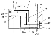
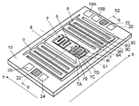
図1に示すように、本実施の形態における光学反射素子60は、ミラー部6と、ミラー部6を介して対向するとともに、ミラー部6の各端部とそれぞれが連結された一対の振動部(第一振動部)7を有している。さらに、これらの振動部7と連結され、振動部7およびミラー部6の外周を囲む枠体8を有している。さらに、枠体8を介して対向するとともに、枠体8の各端部とそれぞれが連結された一対の振動部(第二振動部)9を有している。さらに、これらの振動部9と連結されるとともに、振動部9および枠体8の外周を囲う枠形状の支持体10を有している。
図10は本発明の実施の形態2における光学反射素子の電極パターンを模式的に示した図である。本実施の形態と実施の形態1との主な違いは、図10に示すように、電気的に独立した二つの駆動電極31、32を振動部7に設けた点である。駆動電極31、32には、それぞれ外部電極19A、19Bを介して、正負逆位相の交流電圧を印加する。
図14は、本発明の実施の形態3における光学反射素子の電極パターンを模式的に示した図である。本実施の形態と実施の形態1との違いは、図14に示すように、振動部7および振動部9のモニター素子は、共通のモニター電極33を有し、これらのモニター電極33は、図15に示すように、共通の配線電極33Aで外部電極34から引き出される点である。
図16は、本発明の実施の形態4における圧電駆動装置の構成を示すブロック図である。本実施の形態と実施の形態1との主な違いは、圧電駆動装置に電気信号を合成する合成回路を設けた点である。
7,9 振動部
7A〜7D,9A〜9E 振動板
8 枠体
10 支持体
11 圧電素子
12,13 モニター素子
14 シリコン基板
15 シリコン酸化膜
16 接地電極
17 圧電層
18,31,32,35,36 駆動電極
18A,21A,23A,31A,32A,33A,35A,36A 配線電極
19,19A,19B,20,22,24,34 外部電極
25,26 増幅器
27,28 インピーダンス素子
29,30,37A,37B フィルター
38,39 前置アンプ
40,42 飽和アンプ
41,43 帯域フィルター
44 加算器
45 加算合成回路
46 光源
47 入射光
48 反射光
49 スクリーン
50 画像
60 光学反射素子
61 駆動装置
62 駆動制御装置
S1,S2 中心軸
Claims (7)
- 第一駆動電極を有する第一圧電素子を備えた第一振動部と、前記第一振動部とは方向が異なり交差する中心軸を有し、第二駆動電極を有する第二圧電素子を備えた第二振動部と、前記第一駆動電極および前記第二駆動電極に電気信号を印加する外部電極とを備え、前記外部電極に対して前記第一駆動電極と前記第二駆動電極が順に接続された圧電アクチュエータ。
- 第一駆動電極を有する第一圧電素子を備えた第一振動部と、前記第一振動部とは方向が異なり交差する中心軸を有し、第二駆動電極を有する第二圧電素子を備えた第二振動部と、前記第一駆動電極および前記第二駆動電極に電気信号を印加する外部電極とを備え、前記外部電極に対して前記第一駆動電極と前記第二駆動電極が順に接続され、前記第一駆動電極と前記第二駆動電極に、少なくとも二つの電気信号を合成した電気信号を供給する圧電駆動装置。
- 前記少なくとも二つの電気信号を合成した電気信号は、前記第一振動部を駆動させる第一電気信号と、前記第二振動部を駆動させる第二電気信号とを、それぞれインピーダンス素子を介して合成してなる請求項2に記載の圧電駆動装置。
- 前記第一振動部を駆動させる第一電気信号が入力される第一前置アンプに接続された第一飽和アンプと、前記第一飽和アンプに接続された第一帯域フィルターと、前記第二振動部を駆動させる第二電気信号が入力される第二前置アンプに接続された第二飽和アンプと、前記第二飽和アンプに接続された第二帯域フィルターと、前記第一帯域フィルターおよび前記第二帯域フィルターの出力を合成する合成回路とを備え、前記少なくとも二つの電気信号を合成した電気信号は、前記合成回路から供給される請求項2に記載の圧電駆動装置。
- 請求項1に記載の圧電アクチュエータと、前記第一振動部または前記第二振動部に連結されたミラー部とを備えた光学反射素子。
- 前記ミラー部は前記第一振動部に連結され、前記第一振動部および前記ミラー部の外周を囲い、前記第一振動部に連結された枠体と、前記枠体に前記第二振動部を介して連結された支持体とをさらに備えた請求項5に記載の光学反射素子。
- 前記第一振動部の走査速度は前記第二振動部の走査速度よりも大きく、前記第一駆動電極および前記第二駆動電極は、前記外部電極に対して前記第二駆動電極、前記第一駆動電極の順に接続されていることを特徴とする請求項2に記載の圧電駆動装置。
Priority Applications (1)
| Application Number | Priority Date | Filing Date | Title |
|---|---|---|---|
| JP2009529976A JP5347963B2 (ja) | 2007-08-27 | 2008-08-20 | 圧電アクチュエータおよびこれを用いた光学反射素子および圧電駆動装置 |
Applications Claiming Priority (6)
| Application Number | Priority Date | Filing Date | Title |
|---|---|---|---|
| JP2007219509 | 2007-08-27 | ||
| JP2007219509 | 2007-08-27 | ||
| JP2008020471 | 2008-01-31 | ||
| JP2008020471 | 2008-01-31 | ||
| JP2009529976A JP5347963B2 (ja) | 2007-08-27 | 2008-08-20 | 圧電アクチュエータおよびこれを用いた光学反射素子および圧電駆動装置 |
| PCT/JP2008/002246 WO2009028152A1 (ja) | 2007-08-27 | 2008-08-20 | 圧電アクチュエータおよびこれを用いた光学反射素子および圧電駆動装置 |
Publications (2)
| Publication Number | Publication Date |
|---|---|
| JPWO2009028152A1 JPWO2009028152A1 (ja) | 2010-11-25 |
| JP5347963B2 true JP5347963B2 (ja) | 2013-11-20 |
Family
ID=40386895
Family Applications (1)
| Application Number | Title | Priority Date | Filing Date |
|---|---|---|---|
| JP2009529976A Active JP5347963B2 (ja) | 2007-08-27 | 2008-08-20 | 圧電アクチュエータおよびこれを用いた光学反射素子および圧電駆動装置 |
Country Status (5)
| Country | Link |
|---|---|
| US (1) | US8437061B2 (ja) |
| JP (1) | JP5347963B2 (ja) |
| CN (1) | CN101790840B (ja) |
| TW (1) | TWI470271B (ja) |
| WO (1) | WO2009028152A1 (ja) |
Families Citing this family (24)
| Publication number | Priority date | Publication date | Assignee | Title |
|---|---|---|---|---|
| WO2010122751A1 (ja) * | 2009-04-21 | 2010-10-28 | パナソニック株式会社 | 光学反射素子 |
| JP5444968B2 (ja) | 2009-05-11 | 2014-03-19 | ミツミ電機株式会社 | アクチュエータ及びこれを用いた光走査装置 |
| JP2010263736A (ja) * | 2009-05-11 | 2010-11-18 | Mitsumi Electric Co Ltd | 圧電アクチュエータ |
| JP5611565B2 (ja) * | 2009-10-27 | 2014-10-22 | スタンレー電気株式会社 | 圧電振動発電機及びこれを用いた発電装置 |
| JP5471946B2 (ja) | 2010-08-02 | 2014-04-16 | 船井電機株式会社 | 振動ミラー素子 |
| CN101976013A (zh) * | 2010-09-30 | 2011-02-16 | 上海理工大学 | 具有消除激光散斑的投影机 |
| JP5987510B2 (ja) * | 2011-10-03 | 2016-09-07 | ミツミ電機株式会社 | 光走査装置及び光走査制御装置 |
| JP5779472B2 (ja) * | 2011-10-07 | 2015-09-16 | スタンレー電気株式会社 | 光偏向器 |
| US9287488B2 (en) * | 2012-01-31 | 2016-03-15 | Panasonic Intellectual Property Management Co., Ltd. | Piezoelectric actuator device and method for manufacturing same |
| JP5864311B2 (ja) * | 2012-03-12 | 2016-02-17 | スタンレー電気株式会社 | 光偏向器 |
| JPWO2013136759A1 (ja) | 2012-03-15 | 2015-08-03 | パナソニックIpマネジメント株式会社 | 光学反射素子とアクチュエータ |
| JP2013200337A (ja) * | 2012-03-23 | 2013-10-03 | Stanley Electric Co Ltd | 光偏向器 |
| JP2013205818A (ja) * | 2012-03-29 | 2013-10-07 | Stanley Electric Co Ltd | 光偏向器 |
| US20150270477A1 (en) * | 2012-10-31 | 2015-09-24 | Panasonic Intellectual Property Management Co. | Actuator |
| JP6123290B2 (ja) * | 2012-12-26 | 2017-05-10 | 株式会社リコー | 圧電アクチュエータ装置、2次元走査装置、画像形成装置、及び画像投影装置 |
| JP6264709B2 (ja) * | 2013-12-25 | 2018-01-24 | スタンレー電気株式会社 | 車両用灯具 |
| JP2015132762A (ja) * | 2014-01-15 | 2015-07-23 | 株式会社リコー | 光偏向装置、画像形成装置、及び画像投影装置 |
| JP6398454B2 (ja) | 2014-08-13 | 2018-10-03 | セイコーエプソン株式会社 | 圧電駆動装置、ロボット、及び、それらの駆動方法 |
| EP3304606B1 (en) * | 2015-06-03 | 2019-01-09 | Koninklijke Philips N.V. | Control of actuator device based on an electroactive polymer |
| JP6662392B2 (ja) | 2015-12-22 | 2020-03-11 | 株式会社リコー | 回動装置、光走査装置及び画像表示装置 |
| DE102018215528A1 (de) * | 2018-09-12 | 2020-03-12 | Robert Bosch Gmbh | Mikromechanisches Bauteil und Herstellungsverfahren für ein mikromechanisches Bauteil |
| CN109794405A (zh) * | 2019-02-18 | 2019-05-24 | 河南中医药大学 | 高强度聚焦超声信号校准电路 |
| CN112782845B (zh) * | 2020-12-31 | 2023-02-21 | 歌尔股份有限公司 | Mems扫描镜及激光投影仪 |
| CN112817141B (zh) * | 2020-12-31 | 2023-03-24 | 歌尔股份有限公司 | Mems扫描镜及其驱动方法、激光投影仪 |
Citations (6)
| Publication number | Priority date | Publication date | Assignee | Title |
|---|---|---|---|---|
| JPH09101474A (ja) * | 1995-10-06 | 1997-04-15 | Denso Corp | 光スキャナ装置 |
| JP2001111672A (ja) * | 1999-10-05 | 2001-04-20 | Kenwood Corp | 移動体通信端末 |
| JP2003181800A (ja) * | 2001-12-19 | 2003-07-02 | Hitachi Ltd | 圧電型マイクロアクチュエータ及びこれを備えたマイクロミラー |
| JP2004237400A (ja) * | 2003-02-06 | 2004-08-26 | Nippon Signal Co Ltd:The | プレーナー型アクチュエータ |
| JP2005148459A (ja) * | 2003-11-17 | 2005-06-09 | Stanley Electric Co Ltd | 2次元光スキャナ及び光学装置 |
| JP2008035600A (ja) * | 2006-07-27 | 2008-02-14 | Stanley Electric Co Ltd | 圧電アクチュエータ及びその製造方法 |
Family Cites Families (6)
| Publication number | Priority date | Publication date | Assignee | Title |
|---|---|---|---|---|
| JP3050130B2 (ja) * | 1996-07-31 | 2000-06-12 | 日本電気株式会社 | 圧電トランスおよびその異常動作検出保護装置 |
| JP2003089206A (ja) | 2001-09-19 | 2003-03-25 | Sharp Corp | インクジェットヘッドの駆動方法及びインクジェットプリンタ |
| JP4531470B2 (ja) | 2004-07-26 | 2010-08-25 | Hoya株式会社 | ヒンジ構造 |
| US7356880B2 (en) * | 2004-07-26 | 2008-04-15 | Pentax Corporation | Hinge structure of micromirror device |
| JP4328980B2 (ja) * | 2006-12-18 | 2009-09-09 | セイコーエプソン株式会社 | 圧電振動子およびその製造方法、並びに、memsデバイスおよびその製造方法 |
| JP4317231B2 (ja) | 2007-02-16 | 2009-08-19 | 富士通株式会社 | マイクロミラー素子およびその製造方法 |
-
2008
- 2008-08-20 JP JP2009529976A patent/JP5347963B2/ja active Active
- 2008-08-20 WO PCT/JP2008/002246 patent/WO2009028152A1/ja not_active Ceased
- 2008-08-20 CN CN2008801046486A patent/CN101790840B/zh active Active
- 2008-08-20 US US12/673,238 patent/US8437061B2/en active Active
- 2008-08-25 TW TW97132360A patent/TWI470271B/zh not_active IP Right Cessation
Patent Citations (6)
| Publication number | Priority date | Publication date | Assignee | Title |
|---|---|---|---|---|
| JPH09101474A (ja) * | 1995-10-06 | 1997-04-15 | Denso Corp | 光スキャナ装置 |
| JP2001111672A (ja) * | 1999-10-05 | 2001-04-20 | Kenwood Corp | 移動体通信端末 |
| JP2003181800A (ja) * | 2001-12-19 | 2003-07-02 | Hitachi Ltd | 圧電型マイクロアクチュエータ及びこれを備えたマイクロミラー |
| JP2004237400A (ja) * | 2003-02-06 | 2004-08-26 | Nippon Signal Co Ltd:The | プレーナー型アクチュエータ |
| JP2005148459A (ja) * | 2003-11-17 | 2005-06-09 | Stanley Electric Co Ltd | 2次元光スキャナ及び光学装置 |
| JP2008035600A (ja) * | 2006-07-27 | 2008-02-14 | Stanley Electric Co Ltd | 圧電アクチュエータ及びその製造方法 |
Also Published As
| Publication number | Publication date |
|---|---|
| TWI470271B (zh) | 2015-01-21 |
| TW200925648A (en) | 2009-06-16 |
| US20110122471A1 (en) | 2011-05-26 |
| WO2009028152A1 (ja) | 2009-03-05 |
| US8437061B2 (en) | 2013-05-07 |
| JPWO2009028152A1 (ja) | 2010-11-25 |
| CN101790840B (zh) | 2013-03-20 |
| CN101790840A (zh) | 2010-07-28 |
Similar Documents
| Publication | Publication Date | Title |
|---|---|---|
| JP5347963B2 (ja) | 圧電アクチュエータおよびこれを用いた光学反射素子および圧電駆動装置 | |
| JP5446122B2 (ja) | ミアンダ形振動子およびこれを用いた光学反射素子 | |
| JP5262613B2 (ja) | 光学反射素子 | |
| JP7237146B2 (ja) | マイクロミラーデバイスおよびマイクロミラーデバイスの駆動方法 | |
| JP5293668B2 (ja) | 光学反射素子 | |
| JP5666955B2 (ja) | 光偏向器 | |
| JP2010148265A (ja) | ミアンダ形振動子およびこれを用いた光学反射素子 | |
| JP2012237788A (ja) | 光走査装置およびそれを備えた画像投影装置 | |
| JP5239379B2 (ja) | 光学反射素子 | |
| KR20120006507A (ko) | 광학 반사 소자 | |
| JP2004177543A (ja) | 光走査装置および光走査装置を備えた画像形成装置 | |
| JP2009258210A (ja) | 光学反射素子 | |
| JP2009265560A (ja) | 光学反射素子 | |
| JP2009258339A (ja) | 光学反射素子 | |
| JP2009223115A (ja) | 光学反射素子 | |
| JP5239382B2 (ja) | 光学反射素子 | |
| JP2009244602A (ja) | 光学反射素子 | |
| JP5076526B2 (ja) | 光学反射素子 | |
| JP2009217093A (ja) | 光学反射素子 | |
| JP2009192781A (ja) | 光学反射素子 | |
| JP2010060688A (ja) | 光学反射素子 | |
| JP2015100093A (ja) | 超音波デバイスおよびプローブ並びに電子機器および超音波画像装置 | |
| JP5077139B2 (ja) | 光学反射素子 | |
| JP3776521B2 (ja) | 光スキャナ | |
| JP6221679B2 (ja) | 超音波デバイスおよびプローブ並びに電子機器および超音波画像装置 |
Legal Events
| Date | Code | Title | Description |
|---|---|---|---|
| A521 | Request for written amendment filed |
Free format text: JAPANESE INTERMEDIATE CODE: A523 Effective date: 20110802 |
|
| A621 | Written request for application examination |
Free format text: JAPANESE INTERMEDIATE CODE: A621 Effective date: 20110802 |
|
| RD01 | Notification of change of attorney |
Free format text: JAPANESE INTERMEDIATE CODE: A7421 Effective date: 20121217 |
|
| A131 | Notification of reasons for refusal |
Free format text: JAPANESE INTERMEDIATE CODE: A131 Effective date: 20130423 |
|
| A521 | Request for written amendment filed |
Free format text: JAPANESE INTERMEDIATE CODE: A523 Effective date: 20130614 |
|
| TRDD | Decision of grant or rejection written | ||
| A01 | Written decision to grant a patent or to grant a registration (utility model) |
Free format text: JAPANESE INTERMEDIATE CODE: A01 Effective date: 20130723 |
|
| A61 | First payment of annual fees (during grant procedure) |
Free format text: JAPANESE INTERMEDIATE CODE: A61 Effective date: 20130805 |
|
| R151 | Written notification of patent or utility model registration |
Ref document number: 5347963 Country of ref document: JP Free format text: JAPANESE INTERMEDIATE CODE: R151 |