JP5367383B2 - 表示装置及びその駆動方法 - Google Patents
表示装置及びその駆動方法 Download PDFInfo
- Publication number
- JP5367383B2 JP5367383B2 JP2009005849A JP2009005849A JP5367383B2 JP 5367383 B2 JP5367383 B2 JP 5367383B2 JP 2009005849 A JP2009005849 A JP 2009005849A JP 2009005849 A JP2009005849 A JP 2009005849A JP 5367383 B2 JP5367383 B2 JP 5367383B2
- Authority
- JP
- Japan
- Prior art keywords
- light
- scanning line
- scanning
- display device
- optical waveguide
- Prior art date
- Legal status (The legal status is an assumption and is not a legal conclusion. Google has not performed a legal analysis and makes no representation as to the accuracy of the status listed.)
- Expired - Fee Related
Links
Images


Classifications
-
- G—PHYSICS
- G09—EDUCATION; CRYPTOGRAPHY; DISPLAY; ADVERTISING; SEALS
- G09G—ARRANGEMENTS OR CIRCUITS FOR CONTROL OF INDICATING DEVICES USING STATIC MEANS TO PRESENT VARIABLE INFORMATION
- G09G3/00—Control arrangements or circuits, of interest only in connection with visual indicators other than cathode-ray tubes
- G09G3/20—Control arrangements or circuits, of interest only in connection with visual indicators other than cathode-ray tubes for presentation of an assembly of a number of characters, e.g. a page, by composing the assembly by combination of individual elements arranged in a matrix no fixed position being assigned to or needed to be assigned to the individual characters or partial characters
- G09G3/34—Control arrangements or circuits, of interest only in connection with visual indicators other than cathode-ray tubes for presentation of an assembly of a number of characters, e.g. a page, by composing the assembly by combination of individual elements arranged in a matrix no fixed position being assigned to or needed to be assigned to the individual characters or partial characters by control of light from an independent source
- G09G3/3433—Control arrangements or circuits, of interest only in connection with visual indicators other than cathode-ray tubes for presentation of an assembly of a number of characters, e.g. a page, by composing the assembly by combination of individual elements arranged in a matrix no fixed position being assigned to or needed to be assigned to the individual characters or partial characters by control of light from an independent source using light modulating elements actuated by an electric field and being other than liquid crystal devices and electrochromic devices
- G09G3/3473—Control arrangements or circuits, of interest only in connection with visual indicators other than cathode-ray tubes for presentation of an assembly of a number of characters, e.g. a page, by composing the assembly by combination of individual elements arranged in a matrix no fixed position being assigned to or needed to be assigned to the individual characters or partial characters by control of light from an independent source using light modulating elements actuated by an electric field and being other than liquid crystal devices and electrochromic devices based on light coupled out of a light guide, e.g. due to scattering, by contracting the light guide with external means
-
- G—PHYSICS
- G02—OPTICS
- G02B—OPTICAL ELEMENTS, SYSTEMS OR APPARATUS
- G02B6/00—Light guides; Structural details of arrangements comprising light guides and other optical elements, e.g. couplings
- G02B6/0001—Light guides; Structural details of arrangements comprising light guides and other optical elements, e.g. couplings specially adapted for lighting devices or systems
- G02B6/0005—Light guides; Structural details of arrangements comprising light guides and other optical elements, e.g. couplings specially adapted for lighting devices or systems the light guides being of the fibre type
- G02B6/001—Light guides; Structural details of arrangements comprising light guides and other optical elements, e.g. couplings specially adapted for lighting devices or systems the light guides being of the fibre type the light being emitted along at least a portion of the lateral surface of the fibre
-
- G—PHYSICS
- G02—OPTICS
- G02B—OPTICAL ELEMENTS, SYSTEMS OR APPARATUS
- G02B6/00—Light guides; Structural details of arrangements comprising light guides and other optical elements, e.g. couplings
- G02B6/24—Coupling light guides
- G02B6/26—Optical coupling means
- G02B6/35—Optical coupling means having switching means
- G02B6/351—Optical coupling means having switching means involving stationary waveguides with moving interposed optical elements
- G02B6/3522—Optical coupling means having switching means involving stationary waveguides with moving interposed optical elements the optical element enabling or impairing total internal reflection
-
- G—PHYSICS
- G02—OPTICS
- G02B—OPTICAL ELEMENTS, SYSTEMS OR APPARATUS
- G02B6/00—Light guides; Structural details of arrangements comprising light guides and other optical elements, e.g. couplings
- G02B6/0001—Light guides; Structural details of arrangements comprising light guides and other optical elements, e.g. couplings specially adapted for lighting devices or systems
- G02B6/0011—Light guides; Structural details of arrangements comprising light guides and other optical elements, e.g. couplings specially adapted for lighting devices or systems the light guides being planar or of plate-like form
- G02B6/0033—Means for improving the coupling-out of light from the light guide
- G02B6/0035—Means for improving the coupling-out of light from the light guide provided on the surface of the light guide or in the bulk of it
-
- G—PHYSICS
- G09—EDUCATION; CRYPTOGRAPHY; DISPLAY; ADVERTISING; SEALS
- G09G—ARRANGEMENTS OR CIRCUITS FOR CONTROL OF INDICATING DEVICES USING STATIC MEANS TO PRESENT VARIABLE INFORMATION
- G09G2310/00—Command of the display device
- G09G2310/02—Addressing, scanning or driving the display screen or processing steps related thereto
- G09G2310/0264—Details of driving circuits
- G09G2310/0267—Details of drivers for scan electrodes, other than drivers for liquid crystal, plasma or OLED displays
-
- G—PHYSICS
- G09—EDUCATION; CRYPTOGRAPHY; DISPLAY; ADVERTISING; SEALS
- G09G—ARRANGEMENTS OR CIRCUITS FOR CONTROL OF INDICATING DEVICES USING STATIC MEANS TO PRESENT VARIABLE INFORMATION
- G09G2310/00—Command of the display device
- G09G2310/02—Addressing, scanning or driving the display screen or processing steps related thereto
- G09G2310/0264—Details of driving circuits
- G09G2310/0283—Arrangement of drivers for different directions of scanning
Landscapes
- Physics & Mathematics (AREA)
- General Physics & Mathematics (AREA)
- Optics & Photonics (AREA)
- Engineering & Computer Science (AREA)
- Computer Hardware Design (AREA)
- Theoretical Computer Science (AREA)
- Light Guides In General And Applications Therefor (AREA)
- Devices For Indicating Variable Information By Combining Individual Elements (AREA)
- Mechanical Light Control Or Optical Switches (AREA)
Description
走査は光導波路に対して電界を印加して屈折率を変化させることにより走査位置が決定される。良好な表示性能を維持するためには、適時性に優れた屈折率変化が要求される。
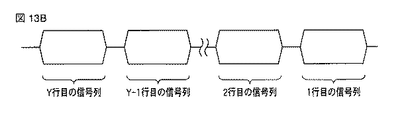
図1は、本発明の一実施形態に係る表示装置の構成例を示す。本表示装置は、光信号を導入するための光源14と、光源14から光を導波するための導光体12と、表示のための走査線11と、走査線11を操作するための走査給電線13と、走査線11と導光体12の各交点に配置された光取出素子15と、光源14と導光体12とを接続するコネクタ16と、光源14及び走査線11を駆動する駆動回路10とを備える。すなわち、本表示装置においては、光源14からの光信号を、導光体12を通して伝播し、走査選択位置において、走査線11に例えば電圧印加を行うことにより光取出素子15を動作させることにより導光体12から光信号を表示面に取り出す。なお、ここで光取出素子15とは、後述するように本実施形態では走査線11からの電気信号により、例えば変位による部材の接触と非接触の制御により導光体12の屈折率を変化させることが可能な素子である。また、図1に示すように、この駆動回路10は、走査線11を光源14からの光信号の伝播方向と逆の方向、つまり光源14から遠い側から順次駆動する。
Claims (12)
- 複数の光源と、
前記光源からの光を導波する複数の光導波路と、
前記光導波路と交差するように配列された複数の走査線と、
前記光導波路と前記走査線との交差部に配置され、前記走査線からの電気信号により前
記光導波路の断面形状に応じて変形可能に前記光導波路と接触することで前記光導波路内
を導波する前記光を外部へ取り出す複数の光取出素子と、
前記走査線を前記光の導波方向と逆の方向に駆動する走査線駆動部と
を具備することを特徴とする表示装置。 - 前記走査線駆動部は、前記光源から遠い走査線から順に駆動することを特徴とする請求
項1記載の表示装置。 - 前記走査線駆動部は、前記走査線を走査選択後に所定のブランク期間を挟んで順次駆動
することを特徴とする請求項1記載の表示装置。 - 前記走査線駆動部は、前記光源に最も近い走査線を駆動した後に、ブランク期間を挟ん
で次の走査線を駆動することを特徴とする請求項1記載の表示装置。 - 前記導波方向に対応する順序で入力される映像信号を前記逆の方向に対応する順序に反
転する反転部と、
前記光源を前記逆の方向に対応する順序の映像信号に従って駆動する光源駆動部と
をさらに具備することを特徴とする請求項1記載の表示装置。 - 前記光導波路は、略円形断面を有することをさらに特徴とする請求項1記載の表示装置
。 - 複数の光源と、前記光源からの光を導波する複数の光導波路と、前記光導波路と交差す
るように配列された複数の走査線と、前記光導波路と前記走査線との交差部に配置され、
前記走査線からの電気信号により前記光導波路の断面形状に応じて変形可能に前記光導波
路と接触することで前記光導波路内を導波する前記光を外部へ取り出す複数の光取出素子
とを備える表示装置を駆動する方法であって、
前記走査線を前記光の導波方向と逆の方向に駆動することを特徴とする駆動方法。 - 前記光源から遠い走査線から順に駆動することを特徴とする請求項7記載の駆動方法。
- 前記走査線を走査選択後に所定のブランク期間を挟んで順次駆動することを特徴とする
請求項7記載の駆動方法。 - 前記光源に最も近い走査線を駆動した後に、ブランク期間を挟んで次の走査線を駆動す
ることを特徴とする請求項7記載の駆動方法。 - 前記光の導波方向に対応する順序で入力される映像信号を前記逆の方向に対応する順序
に反転し、
前記光源を前記逆の方向に対応する順序の映像信号に従って駆動すること
をさらに特徴とする請求項7記載の駆動方法。 - 前記光導波路は、略円形断面を有することをさらに特徴とする請求項7記載の駆動方法
。
Priority Applications (2)
| Application Number | Priority Date | Filing Date | Title |
|---|---|---|---|
| JP2009005849A JP5367383B2 (ja) | 2009-01-14 | 2009-01-14 | 表示装置及びその駆動方法 |
| US12/686,037 US9183794B2 (en) | 2009-01-14 | 2010-01-12 | Display apparatus and driving method thereof |
Applications Claiming Priority (1)
| Application Number | Priority Date | Filing Date | Title |
|---|---|---|---|
| JP2009005849A JP5367383B2 (ja) | 2009-01-14 | 2009-01-14 | 表示装置及びその駆動方法 |
Publications (2)
| Publication Number | Publication Date |
|---|---|
| JP2010164702A JP2010164702A (ja) | 2010-07-29 |
| JP5367383B2 true JP5367383B2 (ja) | 2013-12-11 |
Family
ID=42318732
Family Applications (1)
| Application Number | Title | Priority Date | Filing Date |
|---|---|---|---|
| JP2009005849A Expired - Fee Related JP5367383B2 (ja) | 2009-01-14 | 2009-01-14 | 表示装置及びその駆動方法 |
Country Status (2)
| Country | Link |
|---|---|
| US (1) | US9183794B2 (ja) |
| JP (1) | JP5367383B2 (ja) |
Families Citing this family (10)
| Publication number | Priority date | Publication date | Assignee | Title |
|---|---|---|---|---|
| US20100214282A1 (en) | 2009-02-24 | 2010-08-26 | Dolby Laboratories Licensing Corporation | Apparatus for providing light source modulation in dual modulator displays |
| JP5253461B2 (ja) | 2010-07-26 | 2013-07-31 | 株式会社東芝 | 表示装置 |
| JP5161934B2 (ja) | 2010-08-03 | 2013-03-13 | 株式会社東芝 | 表示素子および表示装置 |
| US9564078B2 (en) | 2010-12-17 | 2017-02-07 | Dolby Laboratories Licensing Corporation | Quantum dots for display panels |
| JP5666945B2 (ja) | 2011-02-28 | 2015-02-12 | 株式会社東芝 | 表示素子および表示装置 |
| JP2013072928A (ja) * | 2011-09-27 | 2013-04-22 | Toshiba Corp | 表示装置 |
| KR102118309B1 (ko) | 2012-09-19 | 2020-06-03 | 돌비 레버러토리즈 라이쎈싱 코오포레이션 | 양자점/리모트 인광 디스플레이 시스템 개선 |
| KR102115146B1 (ko) | 2013-03-08 | 2020-05-26 | 돌비 레버러토리즈 라이쎈싱 코오포레이션 | 광 변환을 갖는 이중 변조 디스플레이 기술들 |
| US10262603B2 (en) | 2014-03-26 | 2019-04-16 | Dolby Laboratories Licensing Corporation | Global light compensation in a variety of displays |
| ES2755506T3 (es) | 2014-08-21 | 2020-04-22 | Dolby Laboratories Licensing Corp | Técnicas para modulación dual con conversión de luz |
Family Cites Families (16)
| Publication number | Priority date | Publication date | Assignee | Title |
|---|---|---|---|---|
| JPH01185692A (ja) | 1988-01-19 | 1989-07-25 | Sanyo Electric Co Ltd | 平面ディスプレイパネル |
| JPH0659295A (ja) * | 1992-08-05 | 1994-03-04 | Fujitsu Ltd | 光走査装置 |
| JP3437743B2 (ja) * | 1997-07-18 | 2003-08-18 | 日本碍子株式会社 | ディスプレイの駆動装置及びディスプレイの駆動方法 |
| JP4074714B2 (ja) * | 1998-09-25 | 2008-04-09 | 富士フイルム株式会社 | アレイ型光変調素子及び平面ディスプレイの駆動方法 |
| JP4460732B2 (ja) * | 2000-07-21 | 2010-05-12 | 富士フイルム株式会社 | 平面表示装置および露光装置 |
| JP2002182203A (ja) * | 2000-12-12 | 2002-06-26 | Nec Corp | 表示装置、その表示方法、およびその製造方法 |
| JP2004118001A (ja) * | 2002-09-27 | 2004-04-15 | Matsushita Electric Ind Co Ltd | 表示装置 |
| WO2004100118A1 (ja) * | 2003-05-07 | 2004-11-18 | Toshiba Matsushita Display Technology Co., Ltd. | El表示装置およびその駆動方法 |
| JP2005227324A (ja) * | 2004-02-10 | 2005-08-25 | Matsushita Electric Ind Co Ltd | 表示素子および表示装置 |
| JP4282533B2 (ja) * | 2004-04-19 | 2009-06-24 | 株式会社東芝 | 表示装置 |
| JP2006030529A (ja) * | 2004-07-15 | 2006-02-02 | Seiko Epson Corp | 電気光学装置用駆動回路及び電気光学装置用駆動方法、並びに電気光学装置及び電子機器 |
| US7545396B2 (en) * | 2005-06-16 | 2009-06-09 | Aurora Systems, Inc. | Asynchronous display driving scheme and display |
| JP2009237375A (ja) * | 2008-03-27 | 2009-10-15 | Toshiba Corp | 表示システムとその表示制御装置及び映像提供装置 |
| JP5044464B2 (ja) * | 2008-03-27 | 2012-10-10 | 株式会社東芝 | 光導波路体 |
| JP5075710B2 (ja) * | 2008-03-28 | 2012-11-21 | 株式会社東芝 | 表示装置 |
| JP5193704B2 (ja) * | 2008-06-30 | 2013-05-08 | 株式会社東芝 | 表示装置 |
-
2009
- 2009-01-14 JP JP2009005849A patent/JP5367383B2/ja not_active Expired - Fee Related
-
2010
- 2010-01-12 US US12/686,037 patent/US9183794B2/en not_active Expired - Fee Related
Also Published As
| Publication number | Publication date |
|---|---|
| US9183794B2 (en) | 2015-11-10 |
| JP2010164702A (ja) | 2010-07-29 |
| US20100177091A1 (en) | 2010-07-15 |
Similar Documents
| Publication | Publication Date | Title |
|---|---|---|
| JP5367383B2 (ja) | 表示装置及びその駆動方法 | |
| US8783931B2 (en) | Light injection system and method for uniform luminosity of waveguide-based displays | |
| US20110013423A1 (en) | Light injection system and method for uniform luminosity of waveguide-based displays | |
| US20070189667A1 (en) | Display element and display device using the same | |
| US20140218971A1 (en) | Display device, joint display and backlight module | |
| US8548289B2 (en) | Apparatus and method for reducing pixel operational voltage in MEMS-based optical displays | |
| JP2000172197A (ja) | 光源内蔵型光導波路ディスプレイおよび光源内蔵型光導波路ディスプレイ装置 | |
| JP2012505498A (ja) | フラットパネルディスプレイのためのキャビティ反射器光注入 | |
| JP2002040339A (ja) | 光変調素子の駆動方法及び光変調素子並びにそれを用いた露光装置、平面表示装置 | |
| JP5075710B2 (ja) | 表示装置 | |
| US6236799B1 (en) | Flat-panel display device using optical waveguide | |
| JP3810788B2 (ja) | 表示装置 | |
| CN104820257A (zh) | 一种导光板、背光源和显示装置 | |
| JP2008197519A (ja) | 表示装置 | |
| JP2004118001A (ja) | 表示装置 | |
| US10295726B2 (en) | Display apparatus | |
| JP2008122572A (ja) | 電気光学素子、電気光学素子の製造方法及び走査型光学装置 | |
| US8390610B2 (en) | Display apparatus with scanning lines having convex and concave portions | |
| JP2010113982A (ja) | 液晶表示装置 | |
| US9116373B2 (en) | Liquid crystal display device including a backlight unit assembly and a bottom cover | |
| JP5475871B2 (ja) | 表示装置 | |
| JP2009151209A (ja) | ディスプレイ装置 | |
| CN107909956B (zh) | 显示器 | |
| US12326624B2 (en) | Display device | |
| KR101424036B1 (ko) | 액정표시장치 및 그 제조방법 |
Legal Events
| Date | Code | Title | Description |
|---|---|---|---|
| A621 | Written request for application examination |
Free format text: JAPANESE INTERMEDIATE CODE: A621 Effective date: 20110426 |
|
| A977 | Report on retrieval |
Free format text: JAPANESE INTERMEDIATE CODE: A971007 Effective date: 20120912 |
|
| A131 | Notification of reasons for refusal |
Free format text: JAPANESE INTERMEDIATE CODE: A131 Effective date: 20120918 |
|
| A521 | Written amendment |
Free format text: JAPANESE INTERMEDIATE CODE: A523 Effective date: 20121119 |
|
| A131 | Notification of reasons for refusal |
Free format text: JAPANESE INTERMEDIATE CODE: A131 Effective date: 20130319 |
|
| A521 | Written amendment |
Free format text: JAPANESE INTERMEDIATE CODE: A523 Effective date: 20130408 |
|
| TRDD | Decision of grant or rejection written | ||
| A01 | Written decision to grant a patent or to grant a registration (utility model) |
Free format text: JAPANESE INTERMEDIATE CODE: A01 Effective date: 20130820 |
|
| A61 | First payment of annual fees (during grant procedure) |
Free format text: JAPANESE INTERMEDIATE CODE: A61 Effective date: 20130911 |
|
| LAPS | Cancellation because of no payment of annual fees |