JP5367662B2 - 液晶組成物、それを用いた液晶パネル、および液晶シャッターメガネ - Google Patents
液晶組成物、それを用いた液晶パネル、および液晶シャッターメガネ Download PDFInfo
- Publication number
- JP5367662B2 JP5367662B2 JP2010196983A JP2010196983A JP5367662B2 JP 5367662 B2 JP5367662 B2 JP 5367662B2 JP 2010196983 A JP2010196983 A JP 2010196983A JP 2010196983 A JP2010196983 A JP 2010196983A JP 5367662 B2 JP5367662 B2 JP 5367662B2
- Authority
- JP
- Japan
- Prior art keywords
- liquid crystal
- polymer
- panel
- voltage
- monomer
- Prior art date
- Legal status (The legal status is an assumption and is not a legal conclusion. Google has not performed a legal analysis and makes no representation as to the accuracy of the status listed.)
- Expired - Fee Related
Links
- HGNVEXMJZVUWJO-UHFFFAOYSA-N CCCC(C)(CC)N Chemical compound CCCC(C)(CC)N HGNVEXMJZVUWJO-UHFFFAOYSA-N 0.000 description 1
Images





Classifications
-
- C—CHEMISTRY; METALLURGY
- C09—DYES; PAINTS; POLISHES; NATURAL RESINS; ADHESIVES; COMPOSITIONS NOT OTHERWISE PROVIDED FOR; APPLICATIONS OF MATERIALS NOT OTHERWISE PROVIDED FOR
- C09K—MATERIALS FOR MISCELLANEOUS APPLICATIONS, NOT PROVIDED FOR ELSEWHERE
- C09K19/00—Liquid crystal materials
- C09K19/02—Liquid crystal materials characterised by optical, electrical or physical properties of the components, in general
- C09K19/0275—Blue phase
-
- C—CHEMISTRY; METALLURGY
- C09—DYES; PAINTS; POLISHES; NATURAL RESINS; ADHESIVES; COMPOSITIONS NOT OTHERWISE PROVIDED FOR; APPLICATIONS OF MATERIALS NOT OTHERWISE PROVIDED FOR
- C09K—MATERIALS FOR MISCELLANEOUS APPLICATIONS, NOT PROVIDED FOR ELSEWHERE
- C09K19/00—Liquid crystal materials
- C09K19/04—Liquid crystal materials characterised by the chemical structure of the liquid crystal components, e.g. by a specific unit
- C09K19/38—Polymers
-
- C—CHEMISTRY; METALLURGY
- C09—DYES; PAINTS; POLISHES; NATURAL RESINS; ADHESIVES; COMPOSITIONS NOT OTHERWISE PROVIDED FOR; APPLICATIONS OF MATERIALS NOT OTHERWISE PROVIDED FOR
- C09K—MATERIALS FOR MISCELLANEOUS APPLICATIONS, NOT PROVIDED FOR ELSEWHERE
- C09K19/00—Liquid crystal materials
- C09K19/52—Liquid crystal materials characterised by components which are not liquid crystals, e.g. additives with special physical aspect: solvents, solid particles
- C09K19/54—Additives having no specific mesophase characterised by their chemical composition
- C09K19/542—Macromolecular compounds
-
- C—CHEMISTRY; METALLURGY
- C09—DYES; PAINTS; POLISHES; NATURAL RESINS; ADHESIVES; COMPOSITIONS NOT OTHERWISE PROVIDED FOR; APPLICATIONS OF MATERIALS NOT OTHERWISE PROVIDED FOR
- C09K—MATERIALS FOR MISCELLANEOUS APPLICATIONS, NOT PROVIDED FOR ELSEWHERE
- C09K19/00—Liquid crystal materials
- C09K19/04—Liquid crystal materials characterised by the chemical structure of the liquid crystal components, e.g. by a specific unit
- C09K2019/0444—Liquid crystal materials characterised by the chemical structure of the liquid crystal components, e.g. by a specific unit characterized by a linking chain between rings or ring systems, a bridging chain between extensive mesogenic moieties or an end chain group
- C09K2019/0448—Liquid crystal materials characterised by the chemical structure of the liquid crystal components, e.g. by a specific unit characterized by a linking chain between rings or ring systems, a bridging chain between extensive mesogenic moieties or an end chain group the end chain group being a polymerizable end group, e.g. -Sp-P or acrylate
Landscapes
- Chemical & Material Sciences (AREA)
- Crystallography & Structural Chemistry (AREA)
- Engineering & Computer Science (AREA)
- Materials Engineering (AREA)
- Organic Chemistry (AREA)
- Liquid Crystal (AREA)
- Stereoscopic And Panoramic Photography (AREA)
- Liquid Crystal Substances (AREA)
Description

図8は、第1の実施例の液晶組成物を液晶層として用いた液晶パネルの斜視図である。液晶パネル1は画素や走査線や信号線などの配線がアレイ状に形成されたアレイ基板10と、所定の間隔でアレイ基板10と対向し、対向電極を有する対向基板20と、アレイ基板10と対向基板20の間に保持され、第1の実施形態で説明した液晶組成物で形成された液晶層30と、を有する。
画素電極105a表面には、絶縁性薄膜(不図示)が形成されている。アレイ基板10と対向基板20との間の距離が、より正確に所定の間隔に保たれるように、アレイ基板10と対向基板20の間にはスペーサー(不図示)が設けられている。
以下、液晶パネルの一実施例について説明する。
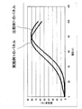
実施例1のパネルの誘電率異方性Δε=33〜50と求められた。一方、比較例1のパネルの誘電率異方性Δε=43〜90と求められた。フッ素置換した高分子を用いることによりセル全体の書き込み電荷量が下がることを確認した。これは、以下の理由によると考えられる。
以下、本発明の実施例について説明する。
Claims (6)
- ブルー相を呈する液晶材料と、
化1で表わされる第1の繰り返し単位を有する高分子と、
を有し、
R1は少なくとも最末端の炭素原子にフッ素原子が結合しているフッ化アルキル基である液晶組成物。
- 前記R1は直鎖のアルキル基である請求項1に記載の液晶組成物。
- 前記第1の繰り返し単位は、化2で表わされる請求項1に記載の液晶組成物。
- 前記高分子は、メソゲン基を含む第2の繰り返し単位を更に備える請求項1乃至3のいずれか1項に記載の液晶組成物。
- アレイ基板と、
前記アレイ基板と対向する対向基板と、
前記アレイ基板と前記対向基板との間に保持され、ブルー相を呈する液晶材料と、化3で表わされる第1の繰り返し単位を有する高分子と、を有し、R1は少なくとも最末端の炭素原子にフッ素原子が結合しているフッ化アルキル基である、液晶層と、
前記液晶層に電圧を印加する電圧印加手段と、
を備える液晶パネル。
- アレイ基板と、
前記アレイ基板と対向する対向基板と、
前記アレイ基板と前記対向基板との間に保持され、ブルー相を呈する液晶材料と、化4で表わされる第1の繰り返し単位を有する高分子と、を有し、R1は少なくとも最末端の炭素原子にフッ素原子が結合しているフッ化アルキル基である、液晶層と、
前記液晶層に電圧を印加する電圧印加手段と、
を備える液晶シャッターメガネ。
Priority Applications (2)
| Application Number | Priority Date | Filing Date | Title |
|---|---|---|---|
| JP2010196983A JP5367662B2 (ja) | 2010-09-02 | 2010-09-02 | 液晶組成物、それを用いた液晶パネル、および液晶シャッターメガネ |
| US13/069,918 US8409468B2 (en) | 2010-09-02 | 2011-03-23 | Liquid crystal composition, liquid crystal panel using the same, and liquid crystal shutter glasses |
Applications Claiming Priority (1)
| Application Number | Priority Date | Filing Date | Title |
|---|---|---|---|
| JP2010196983A JP5367662B2 (ja) | 2010-09-02 | 2010-09-02 | 液晶組成物、それを用いた液晶パネル、および液晶シャッターメガネ |
Publications (2)
| Publication Number | Publication Date |
|---|---|
| JP2012052050A JP2012052050A (ja) | 2012-03-15 |
| JP5367662B2 true JP5367662B2 (ja) | 2013-12-11 |
Family
ID=45770480
Family Applications (1)
| Application Number | Title | Priority Date | Filing Date |
|---|---|---|---|
| JP2010196983A Expired - Fee Related JP5367662B2 (ja) | 2010-09-02 | 2010-09-02 | 液晶組成物、それを用いた液晶パネル、および液晶シャッターメガネ |
Country Status (2)
| Country | Link |
|---|---|
| US (1) | US8409468B2 (ja) |
| JP (1) | JP5367662B2 (ja) |
Families Citing this family (6)
| Publication number | Priority date | Publication date | Assignee | Title |
|---|---|---|---|---|
| JP5367662B2 (ja) * | 2010-09-02 | 2013-12-11 | 株式会社東芝 | 液晶組成物、それを用いた液晶パネル、および液晶シャッターメガネ |
| JP6081829B2 (ja) * | 2012-03-30 | 2017-02-15 | 株式会社半導体エネルギー研究所 | 化合物、液晶組成物、および液晶表示装置 |
| TWI496874B (zh) * | 2012-06-26 | 2015-08-21 | Ind Tech Res Inst | 高分子安定化之光學等向性液晶配方及光學等向性液晶元件 |
| JP5931656B2 (ja) * | 2012-09-05 | 2016-06-08 | 株式会社ジャパンディスプレイ | 液晶表示装置 |
| CN105885871B (zh) * | 2016-02-25 | 2018-05-08 | 江苏和成新材料有限公司 | 一种聚合性液晶组合物 |
| WO2018091940A1 (en) * | 2016-11-18 | 2018-05-24 | Nikon Corporation | Optical component comprising liquid crystals in a blue phase and process for making such optical component |
Family Cites Families (13)
| Publication number | Priority date | Publication date | Assignee | Title |
|---|---|---|---|---|
| JP3779937B2 (ja) | 2002-05-08 | 2006-05-31 | 独立行政法人科学技術振興機構 | 光学変調素子用液晶材料 |
| TWI252341B (en) * | 2004-01-15 | 2006-04-01 | Sharp Kk | Display element, display device, and manufacturing method of display element |
| US20080167482A1 (en) * | 2004-08-10 | 2008-07-10 | Merck Patent Gmbh | Liquid Crystal Compounds, Liquid Crystal Medium and Liquid Crystal Display |
| JP4972858B2 (ja) * | 2004-09-24 | 2012-07-11 | Jnc株式会社 | 高分子と光学活性な液晶材料からなる複合体 |
| CN101080480B (zh) * | 2004-12-17 | 2017-08-08 | 默克专利股份有限公司 | 液晶体系和液晶显示器 |
| EP1690915B1 (en) * | 2005-02-14 | 2008-03-26 | MERCK PATENT GmbH | Mesogenic compounds, liquid crystal medium and liquid crystal display |
| EP2087067B1 (en) * | 2006-11-24 | 2012-06-27 | Merck Patent GmbH | Cyclohexylene reactive mesogens and their applications |
| JP5378696B2 (ja) * | 2007-03-29 | 2013-12-25 | 国立大学法人九州大学 | 高分子/液晶複合材料および液晶表示素子 |
| EP2129743B1 (en) * | 2007-03-30 | 2010-11-10 | Merck Patent GmbH | Birefringent polymer film with negative optical dispersion |
| ATE530621T1 (de) * | 2007-09-25 | 2011-11-15 | Merck Patent Gmbh | Mesogene dimere |
| JP5238571B2 (ja) | 2009-03-25 | 2013-07-17 | 株式会社東芝 | 液晶表示装置 |
| DE102011015546A1 (de) * | 2010-04-26 | 2012-01-26 | Merck Patent Gmbh | Polymerisierbare Verbindungen und ihre Verwendung in Flüssigkristallmedien und Flüssigkristallanzeigen |
| JP5367662B2 (ja) * | 2010-09-02 | 2013-12-11 | 株式会社東芝 | 液晶組成物、それを用いた液晶パネル、および液晶シャッターメガネ |
-
2010
- 2010-09-02 JP JP2010196983A patent/JP5367662B2/ja not_active Expired - Fee Related
-
2011
- 2011-03-23 US US13/069,918 patent/US8409468B2/en not_active Expired - Fee Related
Also Published As
| Publication number | Publication date |
|---|---|
| JP2012052050A (ja) | 2012-03-15 |
| US20120057086A1 (en) | 2012-03-08 |
| US8409468B2 (en) | 2013-04-02 |
Similar Documents
| Publication | Publication Date | Title |
|---|---|---|
| US7576829B2 (en) | Liquid crystal display device | |
| JP5269284B2 (ja) | 高分子とキラリティーを有する液晶材料とからなる複合材料、該複合材料の製造方法、および該複合材料を用いる光素子 | |
| JP5761244B2 (ja) | 液晶組成物 | |
| US20130114010A1 (en) | Polymerisable mixtures and the use thereof in liquid crystal displays | |
| US9771517B2 (en) | Liquid-crystal optical modulation element | |
| CN102031121A (zh) | 液晶组合物和使用其的液晶显示器装置 | |
| US20140313468A1 (en) | Liquid crystal display element | |
| JPH06242429A (ja) | 高分子液晶複合体 | |
| JP5315995B2 (ja) | 液晶光学素子およびその製造方法 | |
| JP2807172B2 (ja) | 液晶光シャッター | |
| US8613985B2 (en) | Liquid crystal/polymer composite | |
| US8409468B2 (en) | Liquid crystal composition, liquid crystal panel using the same, and liquid crystal shutter glasses | |
| JP2010090277A (ja) | 高分子安定化強誘電性液晶組成物、及び液晶素子及び当該表示素子の製造方法 | |
| KR20170072270A (ko) | 중합체를 함유하는 산란형 수직 배향 액정 장치 | |
| JP7024254B2 (ja) | 液晶組成物及び液晶表示素子 | |
| CN100543111C (zh) | 液晶显示元件 | |
| US20120268692A1 (en) | Liquid crystal optical device and its production process | |
| US11434426B2 (en) | Fast flexoelectro-optic switching based on bimesogen-doped and polymer-stabilized vertical standing helix mode | |
| Lim et al. | Fast switching and low operating vertical alignment liquid crystal display with 3-D polymer network for flexible display | |
| JP5594662B2 (ja) | 表示素子、表示素子の製造方法 | |
| JPH08152518A (ja) | 光学異方体フィルムとその製造方法および液晶表示装置 | |
| CN110713838B (zh) | 可聚合液晶组合物和液晶显示器件 | |
| Bigdeli et al. | Polymers in Liquid Crystal Displays (LCDs): Recent Advances and Future Perspectives | |
| TWI514032B (zh) | 製備液晶顯示器之方法 | |
| Chen | Submillisecond-response Blue Phase Liquid Crystals For Display Applications |
Legal Events
| Date | Code | Title | Description |
|---|---|---|---|
| A131 | Notification of reasons for refusal |
Free format text: JAPANESE INTERMEDIATE CODE: A131 Effective date: 20130308 |
|
| A521 | Request for written amendment filed |
Free format text: JAPANESE INTERMEDIATE CODE: A523 Effective date: 20130426 |
|
| A131 | Notification of reasons for refusal |
Free format text: JAPANESE INTERMEDIATE CODE: A131 Effective date: 20130531 |
|
| A521 | Request for written amendment filed |
Free format text: JAPANESE INTERMEDIATE CODE: A523 Effective date: 20130730 |
|
| TRDD | Decision of grant or rejection written | ||
| A01 | Written decision to grant a patent or to grant a registration (utility model) |
Free format text: JAPANESE INTERMEDIATE CODE: A01 Effective date: 20130820 |
|
| A61 | First payment of annual fees (during grant procedure) |
Free format text: JAPANESE INTERMEDIATE CODE: A61 Effective date: 20130911 |
|
| LAPS | Cancellation because of no payment of annual fees |