JP5367666B2 - 誘導ラマン断熱通過の操作方法及び位相ゲート操作の方法 - Google Patents
誘導ラマン断熱通過の操作方法及び位相ゲート操作の方法 Download PDFInfo
- Publication number
- JP5367666B2 JP5367666B2 JP2010211409A JP2010211409A JP5367666B2 JP 5367666 B2 JP5367666 B2 JP 5367666B2 JP 2010211409 A JP2010211409 A JP 2010211409A JP 2010211409 A JP2010211409 A JP 2010211409A JP 5367666 B2 JP5367666 B2 JP 5367666B2
- Authority
- JP
- Japan
- Prior art keywords
- energy
- detuning
- difference
- state
- eigenstate
- Prior art date
- Legal status (The legal status is an assumption and is not a legal conclusion. Google has not performed a legal analysis and makes no representation as to the accuracy of the status listed.)
- Active
Links
Images







Classifications
-
- G—PHYSICS
- G21—NUCLEAR PHYSICS; NUCLEAR ENGINEERING
- G21K—HANDLING OF PARTICLES OR IONISING RADIATION NOT OTHERWISE PROVIDED FOR; IRRADIATION DEVICES; GAMMA RAY OR X-RAY MICROSCOPES
- G21K1/00—Arrangements for handling particles or ionising radiation, e.g. focusing or moderating
- G21K1/30—Arrangements for handling particles or ionising radiation, e.g. focusing or moderating for confining neutral particles or handling confined neutral particles, e.g. atom traps
-
- B—PERFORMING OPERATIONS; TRANSPORTING
- B82—NANOTECHNOLOGY
- B82Y—SPECIFIC USES OR APPLICATIONS OF NANOSTRUCTURES; MEASUREMENT OR ANALYSIS OF NANOSTRUCTURES; MANUFACTURE OR TREATMENT OF NANOSTRUCTURES
- B82Y10/00—Nanotechnology for information processing, storage or transmission, e.g. quantum computing or single electron logic
-
- B—PERFORMING OPERATIONS; TRANSPORTING
- B82—NANOTECHNOLOGY
- B82Y—SPECIFIC USES OR APPLICATIONS OF NANOSTRUCTURES; MEASUREMENT OR ANALYSIS OF NANOSTRUCTURES; MANUFACTURE OR TREATMENT OF NANOSTRUCTURES
- B82Y20/00—Nanooptics, e.g. quantum optics or photonic crystals
-
- B—PERFORMING OPERATIONS; TRANSPORTING
- B82—NANOTECHNOLOGY
- B82B—NANOSTRUCTURES FORMED BY MANIPULATION OF INDIVIDUAL ATOMS, MOLECULES, OR LIMITED COLLECTIONS OF ATOMS OR MOLECULES AS DISCRETE UNITS; MANUFACTURE OR TREATMENT THEREOF
- B82B1/00—Nanostructures formed by manipulation of individual atoms or molecules, or limited collections of atoms or molecules as discrete units
-
- Y—GENERAL TAGGING OF NEW TECHNOLOGICAL DEVELOPMENTS; GENERAL TAGGING OF CROSS-SECTIONAL TECHNOLOGIES SPANNING OVER SEVERAL SECTIONS OF THE IPC; TECHNICAL SUBJECTS COVERED BY FORMER USPC CROSS-REFERENCE ART COLLECTIONS [XRACs] AND DIGESTS
- Y10—TECHNICAL SUBJECTS COVERED BY FORMER USPC
- Y10S—TECHNICAL SUBJECTS COVERED BY FORMER USPC CROSS-REFERENCE ART COLLECTIONS [XRACs] AND DIGESTS
- Y10S977/00—Nanotechnology
- Y10S977/902—Specified use of nanostructure
- Y10S977/932—Specified use of nanostructure for electronic or optoelectronic application
- Y10S977/933—Spintronics or quantum computing
Landscapes
- Engineering & Computer Science (AREA)
- Physics & Mathematics (AREA)
- Chemical & Material Sciences (AREA)
- Nanotechnology (AREA)
- Crystallography & Structural Chemistry (AREA)
- Theoretical Computer Science (AREA)
- Mathematical Physics (AREA)
- General Engineering & Computer Science (AREA)
- High Energy & Nuclear Physics (AREA)
- Spectroscopy & Molecular Physics (AREA)
- Optics & Photonics (AREA)
- Biophysics (AREA)
- Life Sciences & Earth Sciences (AREA)
- Optical Modulation, Optical Deflection, Nonlinear Optics, Optical Demodulation, Optical Logic Elements (AREA)
Description

この際、照射するレーザーの周波数と物質のエネルギー準位差の差である離調が物質のエネルギー準位差に比べて十分小さい共鳴状態で、下準位が上準位へ励起しない効率のよいゲート操作となることが知られている。特に入射する2つのレーザー光と2つのエネルギー準位差の離調同士の差である二光子離調がゼロのとき、すなわち二光子共鳴状態において高効率化することが知られている。
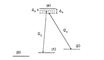
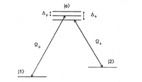
図1に、ここで説明する位相ゲート操作で用いる四準位系(四状態系)を示す。図1に示すように量子ビットに利用する下二準位の状態|0>, |1>と補助的に利用する下準位の状態|2>と励起状態|e>からなる三脚型の四準位系に対し、|1>-|e>, |2>-|e>の各エネルギー準位差に相当する共鳴周波数付近の2本のレーザー光P、Sを照射し量子ビット|0|-|1>間の位相を回転させる。ここで照射するレーザー光P、Sのラビ周波数をΩp,Ωs、離調をΔp, Δsとする。このとき、|0>にはレーザー光が当たらないため位相は固定されるが、|1>の位相はシフトするため、|0>と|1>の間の相対位相がシフトする。そのため|1>, |2>, |e>から成るラムダ型の三準位系(図2)の中で、|1>の位相シフトを考えればよい。
位相シフトを実行する際の三準位系のハミルトニアンは(|1>, |e>, |2>)の順の基底の下で、以下のように表される。
実際の量子状態の時間変化はシュレディンガー方程式を解くことで計算できる。
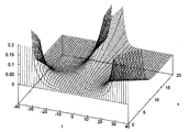
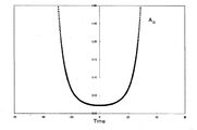
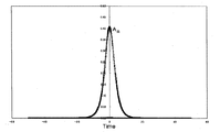
固有状態に沿ってポピュレーション移動するためには断熱条件を満たさなければならない。ダークステートから別の固有状態へ遷移しないようにするためには、固有状態間の固有エネルギー差に比べて十分ゆっくりとした操作をする必要があるが、断熱条件はそのための条件として次式で表される。
非断熱効果Aが小さいほど断熱性がよく断熱条件を満たしやすい。
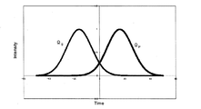
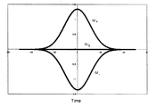
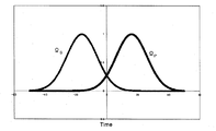
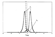
それぞれの固有状態の変化はラビ周波数、つまりレーザー光のパルス設定によって決まる。STIRAPを行う際によく用いられるパルス設定として下記のガウシアンパルスがある。
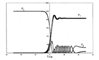
位相シフトにおいても上記STIRAPと同様のハミルトニアンで考えられるが、ポピュレーションを移動しないようなパルス設定が必要になる。位相ゲートのためのパルス波形としては、ポピュレーション移動が生じないようなパルス設定が必要となる。つまり、レーザー照射に伴ってθなど各STIRAPパラメータが変化し、ポピュレーションが初期状態から変化するが、それが元に戻るようなパルス設定である必要がある。そのためには、始状態と終状態で共にθ=0を満たしていれば良い。具体的なパルス設定として次式のような、一定強度とガウシアンパルスから構成されるものが知られている
次に本発明の主要部分である、二光子離調の時間変化によって、位相ゲート操作の断熱性を改善する方法について述べる。
試料として希土類イオン をドープした 結晶(Pr3+:Y2SiO5)を用意し、図27のような の超微細準位を量子ビットに相当する物理系として用いる。この中で誘導ラマン断熱通過に用いる実効的な物理系としては図2のような三準位系であり、照射するレーザー光のラビ周波数をΩ、離調をΔとする。
本実施例では請求項2を実施する場合の例について説明する。
本実施例では請求項3を実施する場合の例について説明する。
試料として希土類イオン をドープした 結晶(Pr3+:Y2SiO5)を用意し、図27のような の超微細準位を量子ビットに相当する物理系として用いる。この中で位相ゲート操作に用いる実効的な物理系としては図1のような四準位系であり、照射するレーザー光のラビ周波数をΩ、離調をΔとする。
本実施例では請求項5を実施する場合について説明する。
110…電気光学効果素子(EOM )
120…音響光学効果素子(AOM)
130…クライオスタット
140…Pr3+:Y2SiO5結晶、150…光検出器
Claims (5)
- エネルギーが低い順に|0>, |1>, |e>からなる三状態系Xで、量子ビットに用いる|0>, |1>に比べ励起状態|e>はエネルギーが高い状態である場合に、|0>−|e>, |1>−|e>の各エネルギー差に相当する共鳴周波数付近の第一、第二のレーザー光をそれぞれ照射し|0>と|1>の確率振幅を変化させる誘導ラマン断熱通過の操作方法であって、
|0>と|e>のエネルギー差と前記第一のレーザー光の周波数差である離調Δpと、|1>と|e>のエネルギー差と前記第二のレーザー光の周波数差である離調Δsの差である二光子離調(Δp−Δs)を時間変化させることを特徴とする誘導ラマン断熱通過の操作方法。 - 前記三状態系Xと同等な性質を有する仮想的な三状態系X’に前記第一、第二のレーザー光と同等な強度を有するレーザー光を照射し、その三状態系X’の固有エネルギー、固有状態、量子状態の時間変化を参照して、三状態系Xに照射する前記第一、第二のレーザー光周波数を時間変化させる誘導ラマン断熱通過の操作方法であって、
前記三状態系Xの「固有エネルギーがEaである固有状態|a>」に対応する前記三状態系X’の「固有エネルギーがEa’である固有状態|a’>」が、その三状態系X’の「固有エネルギーEb’iである他の固有状態|bi’>(i=1,2,3)」に遷移する確率を規定する無次元パラメータである非断熱効果
- 前記誘導ラマン断熱通過の操作中に、固有状態|a’>から励起状態|e>の確率振幅を含む固有状態|ai’>への遷移を表す非断熱効果A(a’,bi’)が、固有状態|a’>から|bi’>より励起状態の確率振幅の割合が小さい固有状態|bj’>への非断熱効果A(a’,bj’)より小さくすることを特徴とする請求項1に記載の誘導ラマン断熱通過の操作方法。
- エネルギーが低い順に|0>, |1> , |2>, |e>からなる四状態系Xで、量子ビットに用いる|0>, |1>と補助的に用いる|2>に比べ励起状態|e>はエネルギーが高い状態である場合に、|1>−|e>, |2>−|e>の各エネルギー差に相当する共鳴周波数付近の第一、第二のレーザー光をそれぞれ照射し|0>と|1>の相対位相を回転させる位相ゲートの操作方法であって、
|1>と|e>のエネルギー差と前記第一のレーザー光の周波数差である離調Δpと、|2>と|e>のエネルギー差と前記第二のレーザー光の周波数差である離調Δsの差である二光子離調(Δp−Δs)を時間変化させることを特徴とする位相ゲートの操作方法。 - 前記四状態系Xと同等な性質を有する仮想的な四状態系Yに前記第一、第二のレーザー光と同等な強度を有する第三、第四のレーザー光を照射し、その四状態系Yの固有エネルギー、固有状態、量子状態の時間変化を参照して、四状態系Xに照射する前記第一、第二のレーザー光の周波数を時間変化させる位相ゲートの操作方法であって、
一定強度の前記第二、第四のレーザー光と時間変化する強度を有する前記第一、第三のレーザー光を用いた|0>−|1>間の相対位相シフト量と|0’>−|1’>間の相対位相シフト量が等しい位相ゲート操作である場合に、前記第一、第三のレーザー光の強度が最大となる時刻で前記二光子離調Δ’p−Δ’s より二光子離調Δp−Δs を大きくすることを特徴とする請求項4に記載の位相ゲートの操作方法。
Priority Applications (2)
| Application Number | Priority Date | Filing Date | Title |
|---|---|---|---|
| JP2010211409A JP5367666B2 (ja) | 2010-09-21 | 2010-09-21 | 誘導ラマン断熱通過の操作方法及び位相ゲート操作の方法 |
| US13/050,628 US8488232B2 (en) | 2010-09-21 | 2011-03-17 | Operating method for stimulated Raman adiabatic passage and operating method for phase gate |
Applications Claiming Priority (1)
| Application Number | Priority Date | Filing Date | Title |
|---|---|---|---|
| JP2010211409A JP5367666B2 (ja) | 2010-09-21 | 2010-09-21 | 誘導ラマン断熱通過の操作方法及び位相ゲート操作の方法 |
Publications (2)
| Publication Number | Publication Date |
|---|---|
| JP2012068329A JP2012068329A (ja) | 2012-04-05 |
| JP5367666B2 true JP5367666B2 (ja) | 2013-12-11 |
Family
ID=45817533
Family Applications (1)
| Application Number | Title | Priority Date | Filing Date |
|---|---|---|---|
| JP2010211409A Active JP5367666B2 (ja) | 2010-09-21 | 2010-09-21 | 誘導ラマン断熱通過の操作方法及び位相ゲート操作の方法 |
Country Status (2)
| Country | Link |
|---|---|
| US (1) | US8488232B2 (ja) |
| JP (1) | JP5367666B2 (ja) |
Families Citing this family (13)
| Publication number | Priority date | Publication date | Assignee | Title |
|---|---|---|---|---|
| CN103515837B (zh) * | 2012-06-21 | 2016-02-03 | 中国科学院大连化学物理研究所 | 一种实现布居数反转的相干绝热受激拉曼激发方法 |
| WO2014164120A1 (en) | 2013-03-12 | 2014-10-09 | 3M Innovative Properties Company | Removal of chlorine and/or chloramine from aqueous solutions |
| JP6223838B2 (ja) * | 2014-01-16 | 2017-11-01 | 株式会社東芝 | 量子計算機及び量子計算方法 |
| US9477796B2 (en) * | 2014-05-23 | 2016-10-25 | The Regents Of The University Of Michigan | Methods for general stabilizer-based quantum computing simulation |
| CN109074518B (zh) * | 2015-12-30 | 2022-09-20 | 谷歌有限责任公司 | 多个本征值的量子相位估计 |
| US10332024B2 (en) | 2017-02-22 | 2019-06-25 | Rigetti & Co, Inc. | Modeling superconducting quantum circuit systems |
| US10504033B1 (en) | 2018-11-13 | 2019-12-10 | Atom Computing Inc. | Scalable neutral atom based quantum computing |
| US11580435B2 (en) | 2018-11-13 | 2023-02-14 | Atom Computing Inc. | Scalable neutral atom based quantum computing |
| US11995512B2 (en) | 2018-11-13 | 2024-05-28 | Atom Computing Inc. | Scalable neutral atom based quantum computing |
| US10892398B2 (en) * | 2019-03-28 | 2021-01-12 | Johannes Pollanen | Qubit hardware for electrons on helium |
| KR102887206B1 (ko) | 2020-03-02 | 2025-11-17 | 아톰 컴퓨팅 인크. | 확장 가능한 중성 원자 기반 양자 컴퓨팅 |
| JP7708774B2 (ja) | 2020-03-02 | 2025-07-15 | アトム コンピューティング インク. | スケーラブルな中性原子ベースの量子コンピューティング |
| EP4526813A4 (en) | 2022-05-19 | 2026-05-06 | Atom Computing Inc | Devices and methods for cavity-based computing |
Family Cites Families (12)
| Publication number | Priority date | Publication date | Assignee | Title |
|---|---|---|---|---|
| JP3576833B2 (ja) * | 1997-09-29 | 2004-10-13 | 株式会社東芝 | 機能素子 |
| JP3854059B2 (ja) * | 1999-11-18 | 2006-12-06 | 株式会社東芝 | 量子情報処理方法および量子情報処理装置 |
| EP1178581A3 (en) * | 2000-07-06 | 2004-09-29 | NEC Research Institute, Inc. | Method and apparatus for gain-assisted superluminal light propagation |
| DE10112625B4 (de) * | 2001-03-14 | 2009-03-05 | Bundesrepublik Deutschland, vertr. d. d. Bundesministerium für Wirtschaft und Technologie, dieses vertr. d. d. Präsidenten der Physikalisch-Technischen Bundesanstalt | Verfahren zur Bildung frequenz- und/oder amplitudenmodulierter elektromagnetischer Pulse zur Induzierung adiabatischer Transfervorgänge in quantenmechanischen Systemen |
| US6795777B1 (en) * | 2002-03-04 | 2004-09-21 | The Texas A&M University System | Identifying molecules of a sample |
| JP4047795B2 (ja) * | 2003-10-31 | 2008-02-13 | 株式会社東芝 | 量子計算方法および量子計算機 |
| JP4599290B2 (ja) * | 2005-12-27 | 2010-12-15 | 株式会社東芝 | 量子情報処理装置および方法 |
| KR20080036794A (ko) * | 2006-10-24 | 2008-04-29 | 함병승 | 광양자로직게이트 |
| JP2009080310A (ja) | 2007-09-26 | 2009-04-16 | Toshiba Corp | 量子計算機および量子計算方法 |
| JP5091717B2 (ja) * | 2008-02-21 | 2012-12-05 | 株式会社東芝 | 量子計算方法および量子計算機 |
| JP5091813B2 (ja) * | 2008-09-17 | 2012-12-05 | 株式会社東芝 | 量子ゲート方法および装置 |
| JP4786727B2 (ja) | 2009-03-27 | 2011-10-05 | 株式会社東芝 | 量子計算方法、量子計算機およびプログラム |
-
2010
- 2010-09-21 JP JP2010211409A patent/JP5367666B2/ja active Active
-
2011
- 2011-03-17 US US13/050,628 patent/US8488232B2/en active Active
Also Published As
| Publication number | Publication date |
|---|---|
| US8488232B2 (en) | 2013-07-16 |
| JP2012068329A (ja) | 2012-04-05 |
| US20120069414A1 (en) | 2012-03-22 |
Similar Documents
| Publication | Publication Date | Title |
|---|---|---|
| JP5367666B2 (ja) | 誘導ラマン断熱通過の操作方法及び位相ゲート操作の方法 | |
| Kim et al. | Ultrafast optical control of entanglement between two quantum-dot spins | |
| He et al. | Coherently driving a single quantum two-level system with dichromatic laser pulses | |
| Grimm et al. | Stabilization and operation of a Kerr-cat qubit | |
| Huet et al. | Deterministic and reconfigurable graph state generation with a single solid-state quantum emitter | |
| Bason et al. | High-fidelity quantum driving | |
| Laird et al. | A valley–spin qubit in a carbon nanotube | |
| Tang et al. | Quantum interference induced photon blockade in a coupled single quantum dot-cavity system | |
| Monz et al. | Realization of universal ion-trap quantum computation with decoherence-free qubits | |
| Dory et al. | Complete coherent control of a quantum dot strongly coupled to a nanocavity | |
| Li et al. | Conditional rotation of two strongly coupled semiconductor charge qubits | |
| JP2014216596A (ja) | 量子ビットの構成方法 | |
| Schneider et al. | Quantum computation with ultracold atoms in a driven optical lattice | |
| Wang et al. | Experimental realization of non-adiabatic universal quantum gates using geometric Landau-Zener-Stückelberg interferometry | |
| Xia et al. | Solid-state optical interconnect between distant superconducting quantum chips | |
| JP2024525383A (ja) | 量子処理素子の電気制御 | |
| Ota et al. | Landau-Zener-Stückelberg interference in coherent charge oscillations of a one-electron double quantum dot | |
| Amini Sabegh et al. | Spatially dependent atom-photon entanglement | |
| Idrees et al. | Manipulation of pulse propagation via tunable electromagnetically induced transparency in a (In, Ga) As/GaAs quantum dot system | |
| Peng et al. | Tunneling induced absorption with competing nonlinearities | |
| Jamil et al. | On-chip generation and guiding of quantum light from a site-controlled quantum dot | |
| Burkard | Diamond spins shining bright | |
| CN116484955A (zh) | 一种构建量子逻辑门的方法及装置 | |
| Sohn et al. | Engineering a diamond spin-qubit with a nano-electro-mechanical system | |
| Kobayashi et al. | Excitation dynamics in a three‐quantum dot system driven by optical near‐field interaction: towards a nanometric photonic device |
Legal Events
| Date | Code | Title | Description |
|---|---|---|---|
| RD04 | Notification of resignation of power of attorney |
Free format text: JAPANESE INTERMEDIATE CODE: A7424 Effective date: 20120106 |
|
| A977 | Report on retrieval |
Free format text: JAPANESE INTERMEDIATE CODE: A971007 Effective date: 20121106 |
|
| A131 | Notification of reasons for refusal |
Free format text: JAPANESE INTERMEDIATE CODE: A131 Effective date: 20121204 |
|
| A521 | Request for written amendment filed |
Free format text: JAPANESE INTERMEDIATE CODE: A523 Effective date: 20121226 |
|
| TRDD | Decision of grant or rejection written | ||
| A01 | Written decision to grant a patent or to grant a registration (utility model) |
Free format text: JAPANESE INTERMEDIATE CODE: A01 Effective date: 20130820 |
|
| A61 | First payment of annual fees (during grant procedure) |
Free format text: JAPANESE INTERMEDIATE CODE: A61 Effective date: 20130911 |
|
| R151 | Written notification of patent or utility model registration |
Ref document number: 5367666 Country of ref document: JP Free format text: JAPANESE INTERMEDIATE CODE: R151 |