JP5370168B2 - 電気光学装置及び電子機器 - Google Patents
電気光学装置及び電子機器 Download PDFInfo
- Publication number
- JP5370168B2 JP5370168B2 JP2010005657A JP2010005657A JP5370168B2 JP 5370168 B2 JP5370168 B2 JP 5370168B2 JP 2010005657 A JP2010005657 A JP 2010005657A JP 2010005657 A JP2010005657 A JP 2010005657A JP 5370168 B2 JP5370168 B2 JP 5370168B2
- Authority
- JP
- Japan
- Prior art keywords
- electro
- liquid crystal
- cooling air
- opening
- optical
- Prior art date
- Legal status (The legal status is an assumption and is not a legal conclusion. Google has not performed a legal analysis and makes no representation as to the accuracy of the status listed.)
- Expired - Fee Related
Links
- 238000001816 cooling Methods 0.000 claims abstract description 115
- 238000011144 upstream manufacturing Methods 0.000 claims abstract description 47
- 239000004973 liquid crystal related substance Substances 0.000 abstract description 105
- 239000000758 substrate Substances 0.000 description 47
- 230000000694 effects Effects 0.000 description 29
- 210000000078 claw Anatomy 0.000 description 8
- 239000010408 film Substances 0.000 description 8
- 230000020169 heat generation Effects 0.000 description 7
- 230000004048 modification Effects 0.000 description 7
- 238000012986 modification Methods 0.000 description 7
- 239000000463 material Substances 0.000 description 5
- 230000000191 radiation effect Effects 0.000 description 5
- 238000005070 sampling Methods 0.000 description 5
- 239000003566 sealing material Substances 0.000 description 5
- 239000011521 glass Substances 0.000 description 4
- 230000017525 heat dissipation Effects 0.000 description 4
- 229910052782 aluminium Inorganic materials 0.000 description 3
- XAGFODPZIPBFFR-UHFFFAOYSA-N aluminium Chemical compound [Al] XAGFODPZIPBFFR-UHFFFAOYSA-N 0.000 description 3
- 239000003086 colorant Substances 0.000 description 3
- 230000007423 decrease Effects 0.000 description 3
- 230000007547 defect Effects 0.000 description 3
- 239000000428 dust Substances 0.000 description 3
- 229910052751 metal Inorganic materials 0.000 description 3
- 239000002184 metal Substances 0.000 description 3
- 238000000034 method Methods 0.000 description 3
- 238000002834 transmittance Methods 0.000 description 3
- 230000009471 action Effects 0.000 description 2
- 238000010586 diagram Methods 0.000 description 2
- 238000004512 die casting Methods 0.000 description 2
- 238000007689 inspection Methods 0.000 description 2
- 238000004519 manufacturing process Methods 0.000 description 2
- 230000007246 mechanism Effects 0.000 description 2
- 230000003287 optical effect Effects 0.000 description 2
- 230000002093 peripheral effect Effects 0.000 description 2
- 239000010453 quartz Substances 0.000 description 2
- VYPSYNLAJGMNEJ-UHFFFAOYSA-N silicon dioxide Inorganic materials O=[Si]=O VYPSYNLAJGMNEJ-UHFFFAOYSA-N 0.000 description 2
- 239000012780 transparent material Substances 0.000 description 2
- 239000004988 Nematic liquid crystal Substances 0.000 description 1
- XUIMIQQOPSSXEZ-UHFFFAOYSA-N Silicon Chemical compound [Si] XUIMIQQOPSSXEZ-UHFFFAOYSA-N 0.000 description 1
- 239000000853 adhesive Substances 0.000 description 1
- 230000001070 adhesive effect Effects 0.000 description 1
- 239000011324 bead Substances 0.000 description 1
- 238000005452 bending Methods 0.000 description 1
- 230000008901 benefit Effects 0.000 description 1
- 230000015572 biosynthetic process Effects 0.000 description 1
- 230000008859 change Effects 0.000 description 1
- 230000006866 deterioration Effects 0.000 description 1
- 238000001962 electrophoresis Methods 0.000 description 1
- 238000005516 engineering process Methods 0.000 description 1
- 239000012530 fluid Substances 0.000 description 1
- 239000003365 glass fiber Substances 0.000 description 1
- 229910052736 halogen Inorganic materials 0.000 description 1
- 150000002367 halogens Chemical class 0.000 description 1
- AMGQUBHHOARCQH-UHFFFAOYSA-N indium;oxotin Chemical compound [In].[Sn]=O AMGQUBHHOARCQH-UHFFFAOYSA-N 0.000 description 1
- 230000007257 malfunction Effects 0.000 description 1
- 239000011159 matrix material Substances 0.000 description 1
- 239000007769 metal material Substances 0.000 description 1
- 238000003825 pressing Methods 0.000 description 1
- 239000011347 resin Substances 0.000 description 1
- 229920005989 resin Polymers 0.000 description 1
- 238000007789 sealing Methods 0.000 description 1
- 229910052710 silicon Inorganic materials 0.000 description 1
- 239000010703 silicon Substances 0.000 description 1
- 229910052709 silver Inorganic materials 0.000 description 1
- 239000004332 silver Substances 0.000 description 1
- 238000005507 spraying Methods 0.000 description 1
- 229910001220 stainless steel Inorganic materials 0.000 description 1
- 239000010935 stainless steel Substances 0.000 description 1
- 238000003786 synthesis reaction Methods 0.000 description 1
- 239000010409 thin film Substances 0.000 description 1
- XLYOFNOQVPJJNP-UHFFFAOYSA-N water Substances O XLYOFNOQVPJJNP-UHFFFAOYSA-N 0.000 description 1
Images


Landscapes
- Liquid Crystal (AREA)
- Projection Apparatus (AREA)
- Devices For Indicating Variable Information By Combining Individual Elements (AREA)
Description
本発明の電気光学装置に係る実施形態について、図1から図15を参照して説明する。尚、以下の実施形態では、本発明の電気光学装置として、駆動回路内蔵型のTFT(Thin Film Transistor)アクティブマトリクス駆動方式の液晶装置を例に挙げて説明する。
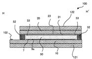
先ず、第1実施形態に係る液晶装置の全体構成について、図3から図7を参照して説明する。ここに図3は、第1実施形態に係る液晶装置を光入射側から見た平面図であり、図4は、第1実施形態に係る液晶装置を光出射側から見た平面図である。また図5は、第1実施形態に係る液晶装置を実装ケースの側面側から見た側面図であり、図6は、図5に示す液晶装置を、実装ケースの主要な構成要素ごとに分解した分解側面図である。図7は、図3に示すA0−A0'線における液晶装置の断面部分の構成を示す断面図である。
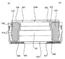
次に、第2実施形態に係る液晶装置について、図12から図14を参照して説明する。ここに図12は、第2実施形態に係る液晶装置を実装ケースの側面側から見た側面図である。また図13及び図14は夫々、第2実施形態に係る液晶装置の変形例を示す側面図である。尚、図12以降の図では、説明の便宜上、図11までに図示した詳細な部材を適宜省略して簡略的に図示している。第2実施形態は、上述の第1実施形態と比べて、実装ケース600の一部の構成が異なり、その他の構成については概ね同様である。このため第2実施形態では、第1実施形態と異なる部分について詳細に説明し、その他の重複する部分については適宜説明を省略する。
次に、第3実施形態に係る液晶装置について、図15を参照して説明する。ここに図15は、第3実施形態に係る液晶装置を実装ケースの側面側から見た側面図である。尚、第3実施形態は、上述の第1及び第2実施形態と比べて、実装ケース600の一部の構成が異なり、その他の構成については概ね同様である。このため第3実施形態では、第1及び第2実施形態と異なる部分について詳細に説明し、その他の重複する部分については適宜説明を省略する。
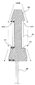
次に、上述した電気光学装置の一例である液晶装置を各種の電子機器に適用する場合について説明する。以下では、この液晶装置をライトバルブとして用いたプロジェクターについて説明する。ここに図16は、プロジェクターの構成例を示す平面図である。また図17及び図18は夫々、図16に示すプロジェクターにおける液晶装置の配置構成を概略的に示す平面図である。
Claims (6)
- 画像を表示する表示部を有する電気光学パネルと、
前記電気光学パネルを少なくとも部分的に覆うと共に、前記表示部を開口部から露出させるように保持する保持部材と
を備え、
前記開口部は、冷却風の上流側に位置する第1辺及び前記第1辺と対向しており前記第1辺より前記冷却風の下流側に位置する第2辺を有し、
前記第1辺の長さは、前記第2辺の長さよりも長い
ことを特徴とする電気光学装置。 - 前記開口部は、前記第2辺を上底とし、前記第1辺を下底とする台形であることを特徴とする請求項1に記載の電気光学装置。
- 前記保持部材は、前記電気光学パネルを光の入射側から覆う第1部材、及び前記電気光学パネルを前記第1部材の反対側から覆う第2部材を有することを特徴とする請求項1又は2に記載の電気光学装置。
- 前記保持部材は、前記開口部から見て前記第2辺側に、前記開口部が設けられた面から盛り上がるように形成された凸部を有することを特徴とする請求項1から3のいずれか一項に記載の電気光学装置。
- 前記保持部材は、前記開口部から見て前記第1辺側の厚みよりも、前記第2辺側の厚みの方が厚くなるように形成されていることを特徴とする請求項1から4のいずれか一項に記載の電気光学装置。
- 請求項1から5のいずれか一項に記載の電気光学装置を具備してなることを特徴とする電子機器。
Priority Applications (1)
| Application Number | Priority Date | Filing Date | Title |
|---|---|---|---|
| JP2010005657A JP5370168B2 (ja) | 2010-01-14 | 2010-01-14 | 電気光学装置及び電子機器 |
Applications Claiming Priority (1)
| Application Number | Priority Date | Filing Date | Title |
|---|---|---|---|
| JP2010005657A JP5370168B2 (ja) | 2010-01-14 | 2010-01-14 | 電気光学装置及び電子機器 |
Publications (2)
| Publication Number | Publication Date |
|---|---|
| JP2011145444A JP2011145444A (ja) | 2011-07-28 |
| JP5370168B2 true JP5370168B2 (ja) | 2013-12-18 |
Family
ID=44460358
Family Applications (1)
| Application Number | Title | Priority Date | Filing Date |
|---|---|---|---|
| JP2010005657A Expired - Fee Related JP5370168B2 (ja) | 2010-01-14 | 2010-01-14 | 電気光学装置及び電子機器 |
Country Status (1)
| Country | Link |
|---|---|
| JP (1) | JP5370168B2 (ja) |
Family Cites Families (4)
| Publication number | Priority date | Publication date | Assignee | Title |
|---|---|---|---|---|
| JP3577698B2 (ja) * | 2001-08-03 | 2004-10-13 | 日本航空電子工業株式会社 | 液晶表示装置 |
| JP4145595B2 (ja) * | 2002-07-30 | 2008-09-03 | 株式会社東芝 | 液晶プロジェクタ |
| JP3092509U (ja) * | 2002-09-02 | 2003-03-20 | 船井電機株式会社 | Dmdを用いた画像表示プロジェクタ |
| JP2006301256A (ja) * | 2005-04-20 | 2006-11-02 | Sony Corp | 回路基板を用いた装置および電子機器 |
-
2010
- 2010-01-14 JP JP2010005657A patent/JP5370168B2/ja not_active Expired - Fee Related
Also Published As
| Publication number | Publication date |
|---|---|
| JP2011145444A (ja) | 2011-07-28 |
Similar Documents
| Publication | Publication Date | Title |
|---|---|---|
| JP5504557B2 (ja) | 電気光学装置及び電気光学装置用実装ケース、並びに電子機器 | |
| JP5533001B2 (ja) | 電気光学装置及び電子機器 | |
| US8373806B2 (en) | Electro-optical device and electronic apparatus | |
| CN102193220B (zh) | 电光装置及电子设备 | |
| JP2010102219A (ja) | 電気光学装置及び電子機器 | |
| JP5109713B2 (ja) | 電気光学装置及び電子機器 | |
| JP5544749B2 (ja) | 電気光学装置及び電子機器 | |
| JP2010256666A (ja) | 電気光学装置及び電子機器 | |
| JP5287119B2 (ja) | 電気光学装置及び電子機器 | |
| JP5370168B2 (ja) | 電気光学装置及び電子機器 | |
| JP2010256662A (ja) | 電気光学装置及び電子機器 | |
| JP2010256667A (ja) | 電気光学装置及び電子機器 | |
| JP2007279626A (ja) | 電気光学装置、及びこれを備えた電子機器 | |
| JP2011145445A (ja) | 電気光学装置及び電子機器 | |
| JP2010256663A (ja) | 電気光学装置及び電子機器 | |
| JP2011145446A (ja) | 電気光学装置及び電子機器 | |
| JP5834402B2 (ja) | 電気光学装置及び電子機器 | |
| JP6269749B2 (ja) | 電気光学装置及び電子機器 | |
| JP5994907B2 (ja) | 電気光学装置及び電子機器 | |
| JP5332482B2 (ja) | 電気光学装置及び電子機器 | |
| JP2009128665A (ja) | 電気光学装置及び電子機器 | |
| JP2010113187A (ja) | 電気光学装置及び電子機器 | |
| JP2010060968A (ja) | 電気光学装置及び電子機器 | |
| JP2009075389A (ja) | 電気光学装置及び電子機器 | |
| JP2010175889A (ja) | 電気光学装置及び電子機器 |
Legal Events
| Date | Code | Title | Description |
|---|---|---|---|
| A621 | Written request for application examination |
Free format text: JAPANESE INTERMEDIATE CODE: A621 Effective date: 20121227 |
|
| A977 | Report on retrieval |
Free format text: JAPANESE INTERMEDIATE CODE: A971007 Effective date: 20130809 |
|
| TRDD | Decision of grant or rejection written | ||
| A01 | Written decision to grant a patent or to grant a registration (utility model) |
Free format text: JAPANESE INTERMEDIATE CODE: A01 Effective date: 20130820 |
|
| A61 | First payment of annual fees (during grant procedure) |
Free format text: JAPANESE INTERMEDIATE CODE: A61 Effective date: 20130902 |
|
| R150 | Certificate of patent or registration of utility model |
Ref document number: 5370168 Country of ref document: JP Free format text: JAPANESE INTERMEDIATE CODE: R150 Free format text: JAPANESE INTERMEDIATE CODE: R150 |
|
| S531 | Written request for registration of change of domicile |
Free format text: JAPANESE INTERMEDIATE CODE: R313531 |
|
| R350 | Written notification of registration of transfer |
Free format text: JAPANESE INTERMEDIATE CODE: R350 |
|
| LAPS | Cancellation because of no payment of annual fees |