JP5372618B2 - パターン付き基板検査装置およびパターン付き基板検査方法 - Google Patents
パターン付き基板検査装置およびパターン付き基板検査方法 Download PDFInfo
- Publication number
- JP5372618B2 JP5372618B2 JP2009154536A JP2009154536A JP5372618B2 JP 5372618 B2 JP5372618 B2 JP 5372618B2 JP 2009154536 A JP2009154536 A JP 2009154536A JP 2009154536 A JP2009154536 A JP 2009154536A JP 5372618 B2 JP5372618 B2 JP 5372618B2
- Authority
- JP
- Japan
- Prior art keywords
- inspection
- pattern
- light
- area
- inspection area
- Prior art date
- Legal status (The legal status is an assumption and is not a legal conclusion. Google has not performed a legal analysis and makes no representation as to the accuracy of the status listed.)
- Expired - Fee Related
Links
Images




Landscapes
- Investigating Materials By The Use Of Optical Means Adapted For Particular Applications (AREA)
Description
102 光源
103 反射ミラー
104 照明光
105 検出光学系
106 集光レンズ
107 偏光板
108 光電変換器
109 A/D変換部
110 判定部
111 全体制御部
112 ステージコントローラ
113 ウェーハ
114 ステージ
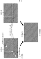
201,304,404 異物またはショート
202 ヒロックまたはグレイン
203,305,405 異物
204 メモリセル部のL/Sパターン
205 大きなパターン部
206 ベア部
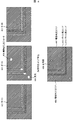
301,401 ダイA
302,402 ダイB
303,406 差画像
306 大きなパターン部エッジ
307 エルボー部
403 ダイC
407,408 輝度判定エリア
409,410 ダイ比較エリア
601 検査モード
602 検査スタートボタン
603 検査条件設定画面
Claims (8)
- 被検査物の表面上の個所に所望の光で照明する照明部と、
前記被検査物からの散乱光を集光する集光光学系と、
前記集光光学系で集光された散乱光を受光して輝度信号に変換する受光部と、
前記輝度信号に基づいて前記被検査物上の欠陥を検出する検出部を有し、
前記照明光はS偏光ビームであり、
前記受光部はP偏光を検出する検光部を備え、
前記検出部において、検査エリアを、前記検光部が欠陥の誤検出を抑えられる検査エリ
アと抑えられない検査エリアに弁別し、
この2つのエリアを別々の検査処理を行い、
前記欠陥の誤検出が抑えられる検査エリアは、照明光の波長以下のパターン幅を有するパターンであるメモリセル部と、パターンの無いベア部であり、
欠陥の誤検出が抑えられない検査エリアは、照明光の波長より大きなパターン幅を有するパターン部のエッジ部分における角度90°のエルボー部であることを特徴とするパターン付き基板検査装置。 - 請求項1において、
所定の基準に基づいて、前記検査エリアを弁別することを特徴とするパターン付き基板検査装置。 - 請求項2において、
前記所定の基準が、3つの検査ダイの少なくとも一部の画像に基づいて、作成されることを特徴とするパターン付き基板検査装置。 - 請求項2において、
過去のデータである経験値を記憶する登録部を有し、 前記所定の基準が、過去のデータである経験値に基づいて作成される、パターン付き基板検査装置。 - 被検査物の表面上の個所に所望の光で照明し、
前記被検査物からの散乱光を集光し、
前記集光された散乱光を受光して輝度信号に変換し、
前記輝度信号に基づいて前記被検査物上の欠陥を検出するパターン付き基板検査方法であって、
前記照明の光はS偏光ビームであり、前記受光はP偏光を検出し、 前記検出において、前記被検査物上の検査エリアを、欠陥の誤検出を抑えられる検査エリアと抑えられない検査エリアに弁別し、
この2つのエリアにおいて、別々の検査処理を行い、
前記欠陥の誤検出が抑えられる検査エリアは、照明光の波長以下のパターン幅を有するパターンであるメモリセル部と、パターンの無いベア部であり、
欠陥の誤検出が抑えられない検査エリアは、照明光の波長より大きなパターン幅を有するパターン部のエッジ部分における角度90°のエルボー部であることを特徴とするパターン付き基板検査方法。 - 請求項5において、
所定の基準に基づいて、前記検査エリアを弁別することを特徴とするパターン付き基板検査方法。 - 請求項6において、
前記所定の基準が、3つの検査ダイの少なくとも一部の画像に基づいて作成されることを特徴とするパターン付き基板検査方法。 - 請求項6において、
過去のデータである経験値を記憶し、
前記所定の基準が、過去のデータである経験値に基づいて作成されることを特徴とするパターン付き基板検査方法。
Priority Applications (1)
| Application Number | Priority Date | Filing Date | Title |
|---|---|---|---|
| JP2009154536A JP5372618B2 (ja) | 2009-06-30 | 2009-06-30 | パターン付き基板検査装置およびパターン付き基板検査方法 |
Applications Claiming Priority (1)
| Application Number | Priority Date | Filing Date | Title |
|---|---|---|---|
| JP2009154536A JP5372618B2 (ja) | 2009-06-30 | 2009-06-30 | パターン付き基板検査装置およびパターン付き基板検査方法 |
Publications (2)
| Publication Number | Publication Date |
|---|---|
| JP2011012966A JP2011012966A (ja) | 2011-01-20 |
| JP5372618B2 true JP5372618B2 (ja) | 2013-12-18 |
Family
ID=43592041
Family Applications (1)
| Application Number | Title | Priority Date | Filing Date |
|---|---|---|---|
| JP2009154536A Expired - Fee Related JP5372618B2 (ja) | 2009-06-30 | 2009-06-30 | パターン付き基板検査装置およびパターン付き基板検査方法 |
Country Status (1)
| Country | Link |
|---|---|
| JP (1) | JP5372618B2 (ja) |
Family Cites Families (6)
| Publication number | Priority date | Publication date | Assignee | Title |
|---|---|---|---|---|
| JPS6270739A (ja) * | 1985-09-25 | 1987-04-01 | Hitachi Electronics Eng Co Ltd | 異物検査装置 |
| JP3087384B2 (ja) * | 1991-10-08 | 2000-09-11 | 松下電器産業株式会社 | 異物検査装置 |
| JPH05134393A (ja) * | 1991-11-13 | 1993-05-28 | Seiko Epson Corp | 異物検査装置及び半導体装置の製造方法 |
| JP4996856B2 (ja) * | 2006-01-23 | 2012-08-08 | 株式会社日立ハイテクノロジーズ | 欠陥検査装置およびその方法 |
| JP4622933B2 (ja) * | 2006-05-15 | 2011-02-02 | 株式会社ニコン | 表面検査方法及び表面検査装置 |
| JP2008051666A (ja) * | 2006-08-25 | 2008-03-06 | Hitachi High-Technologies Corp | 欠陥検査装置 |
-
2009
- 2009-06-30 JP JP2009154536A patent/JP5372618B2/ja not_active Expired - Fee Related
Also Published As
| Publication number | Publication date |
|---|---|
| JP2011012966A (ja) | 2011-01-20 |
Similar Documents
| Publication | Publication Date | Title |
|---|---|---|
| JP4351522B2 (ja) | パターン欠陥検査装置およびパターン欠陥検査方法 | |
| CN104854677B (zh) | 使用缺陷特定的信息检测晶片上的缺陷 | |
| US8472697B2 (en) | Method and apparatus for visual inspection | |
| JP2008203034A (ja) | 欠陥検出装置および欠陥検出方法 | |
| JP2010025713A (ja) | 欠陥検査方法及び欠陥検査装置 | |
| JP3647416B2 (ja) | パターン検査装置及びその方法 | |
| JP2014035326A (ja) | 欠陥検査装置 | |
| WO2010113228A1 (ja) | 検査装置及び検査方法 | |
| JPWO2007132925A1 (ja) | 表面検査装置 | |
| JP4851960B2 (ja) | 異物検査方法、および異物検査装置 | |
| JP2009097928A (ja) | 欠陥検査装置及び欠陥検査方法 | |
| JPH05100413A (ja) | 異物検査装置 | |
| JP2001183301A (ja) | 欠陥検査装置及び方法 | |
| US20100321677A1 (en) | Surface inspecting apparatus and surface inspecting method | |
| JP3878340B2 (ja) | パターンの欠陥検査方法およびその装置 | |
| JP4910128B2 (ja) | 対象物表面の欠陥検査方法 | |
| JP5257063B2 (ja) | 欠陥検出方法および欠陥検出装置 | |
| JP2009103494A (ja) | 表面検査装置 | |
| JP5372618B2 (ja) | パターン付き基板検査装置およびパターン付き基板検査方法 | |
| JP2007093330A (ja) | 欠陥抽出装置及び欠陥抽出方法 | |
| JP5094769B2 (ja) | ウエハの検査方法、ウエハ検査装置および半導体集積回路装置の製造方法 | |
| JP2002303588A (ja) | パターン欠陥検査装置 | |
| JP2010190740A (ja) | 基板検査装置、方法およびプログラム | |
| JP2011185715A (ja) | 検査装置及び検査方法 | |
| JP4967132B2 (ja) | 対象物表面の欠陥検査方法 |
Legal Events
| Date | Code | Title | Description |
|---|---|---|---|
| A621 | Written request for application examination |
Free format text: JAPANESE INTERMEDIATE CODE: A621 Effective date: 20110803 |
|
| A521 | Written amendment |
Free format text: JAPANESE INTERMEDIATE CODE: A523 Effective date: 20110803 |
|
| A977 | Report on retrieval |
Free format text: JAPANESE INTERMEDIATE CODE: A971007 Effective date: 20121003 |
|
| A131 | Notification of reasons for refusal |
Free format text: JAPANESE INTERMEDIATE CODE: A131 Effective date: 20121016 |
|
| A521 | Written amendment |
Free format text: JAPANESE INTERMEDIATE CODE: A523 Effective date: 20121128 |
|
| A131 | Notification of reasons for refusal |
Free format text: JAPANESE INTERMEDIATE CODE: A131 Effective date: 20130604 |
|
| A521 | Written amendment |
Free format text: JAPANESE INTERMEDIATE CODE: A523 Effective date: 20130712 |
|
| TRDD | Decision of grant or rejection written | ||
| A01 | Written decision to grant a patent or to grant a registration (utility model) |
Free format text: JAPANESE INTERMEDIATE CODE: A01 Effective date: 20130820 |
|
| A61 | First payment of annual fees (during grant procedure) |
Free format text: JAPANESE INTERMEDIATE CODE: A61 Effective date: 20130918 |
|
| R150 | Certificate of patent or registration of utility model |
Free format text: JAPANESE INTERMEDIATE CODE: R150 |
|
| LAPS | Cancellation because of no payment of annual fees |