JP5374512B2 - Method for making conductive mechanical interconnect members - Google Patents
Method for making conductive mechanical interconnect members Download PDFInfo
- Publication number
- JP5374512B2 JP5374512B2 JP2010530510A JP2010530510A JP5374512B2 JP 5374512 B2 JP5374512 B2 JP 5374512B2 JP 2010530510 A JP2010530510 A JP 2010530510A JP 2010530510 A JP2010530510 A JP 2010530510A JP 5374512 B2 JP5374512 B2 JP 5374512B2
- Authority
- JP
- Japan
- Prior art keywords
- wire
- presents
- electronic device
- dimensional electronic
- diameter
- Prior art date
- Legal status (The legal status is an assumption and is not a legal conclusion. Google has not performed a legal analysis and makes no representation as to the accuracy of the status listed.)
- Expired - Fee Related
Links
Images


Classifications
-
- H—ELECTRICITY
- H10—SEMICONDUCTOR DEVICES; ELECTRIC SOLID-STATE DEVICES NOT OTHERWISE PROVIDED FOR
- H10W—GENERIC PACKAGES, INTERCONNECTIONS, CONNECTORS OR OTHER CONSTRUCTIONAL DETAILS OF DEVICES COVERED BY CLASS H10
- H10W10/00—Isolation regions in semiconductor bodies between components of integrated devices
-
- B—PERFORMING OPERATIONS; TRANSPORTING
- B82—NANOTECHNOLOGY
- B82Y—SPECIFIC USES OR APPLICATIONS OF NANOSTRUCTURES; MEASUREMENT OR ANALYSIS OF NANOSTRUCTURES; MANUFACTURE OR TREATMENT OF NANOSTRUCTURES
- B82Y10/00—Nanotechnology for information processing, storage or transmission, e.g. quantum computing or single electron logic
-
- B—PERFORMING OPERATIONS; TRANSPORTING
- B82—NANOTECHNOLOGY
- B82Y—SPECIFIC USES OR APPLICATIONS OF NANOSTRUCTURES; MEASUREMENT OR ANALYSIS OF NANOSTRUCTURES; MANUFACTURE OR TREATMENT OF NANOSTRUCTURES
- B82Y40/00—Manufacture or treatment of nanostructures
-
- H—ELECTRICITY
- H10—SEMICONDUCTOR DEVICES; ELECTRIC SOLID-STATE DEVICES NOT OTHERWISE PROVIDED FOR
- H10W—GENERIC PACKAGES, INTERCONNECTIONS, CONNECTORS OR OTHER CONSTRUCTIONAL DETAILS OF DEVICES COVERED BY CLASS H10
- H10W10/00—Isolation regions in semiconductor bodies between components of integrated devices
- H10W10/01—Manufacture or treatment
-
- H—ELECTRICITY
- H10—SEMICONDUCTOR DEVICES; ELECTRIC SOLID-STATE DEVICES NOT OTHERWISE PROVIDED FOR
- H10W—GENERIC PACKAGES, INTERCONNECTIONS, CONNECTORS OR OTHER CONSTRUCTIONAL DETAILS OF DEVICES COVERED BY CLASS H10
- H10W40/00—Arrangements for thermal protection or thermal control
- H10W40/40—Arrangements for thermal protection or thermal control involving heat exchange by flowing fluids
- H10W40/47—Arrangements for thermal protection or thermal control involving heat exchange by flowing fluids by flowing liquids, e.g. forced water cooling
-
- H—ELECTRICITY
- H10—SEMICONDUCTOR DEVICES; ELECTRIC SOLID-STATE DEVICES NOT OTHERWISE PROVIDED FOR
- H10W—GENERIC PACKAGES, INTERCONNECTIONS, CONNECTORS OR OTHER CONSTRUCTIONAL DETAILS OF DEVICES COVERED BY CLASS H10
- H10W72/00—Interconnections or connectors in packages
-
- H—ELECTRICITY
- H10—SEMICONDUCTOR DEVICES; ELECTRIC SOLID-STATE DEVICES NOT OTHERWISE PROVIDED FOR
- H10W—GENERIC PACKAGES, INTERCONNECTIONS, CONNECTORS OR OTHER CONSTRUCTIONAL DETAILS OF DEVICES COVERED BY CLASS H10
- H10W72/00—Interconnections or connectors in packages
- H10W72/01—Manufacture or treatment
-
- H—ELECTRICITY
- H10—SEMICONDUCTOR DEVICES; ELECTRIC SOLID-STATE DEVICES NOT OTHERWISE PROVIDED FOR
- H10W—GENERIC PACKAGES, INTERCONNECTIONS, CONNECTORS OR OTHER CONSTRUCTIONAL DETAILS OF DEVICES COVERED BY CLASS H10
- H10W90/00—Package configurations
-
- H—ELECTRICITY
- H10—SEMICONDUCTOR DEVICES; ELECTRIC SOLID-STATE DEVICES NOT OTHERWISE PROVIDED FOR
- H10D—INORGANIC ELECTRIC SEMICONDUCTOR DEVICES
- H10D64/00—Electrodes of devices having potential barriers
- H10D64/20—Electrodes characterised by their shapes, relative sizes or dispositions
- H10D64/205—Nanosized electrodes, e.g. nanowire electrodes
-
- H—ELECTRICITY
- H10—SEMICONDUCTOR DEVICES; ELECTRIC SOLID-STATE DEVICES NOT OTHERWISE PROVIDED FOR
- H10W—GENERIC PACKAGES, INTERCONNECTIONS, CONNECTORS OR OTHER CONSTRUCTIONAL DETAILS OF DEVICES COVERED BY CLASS H10
- H10W20/00—Interconnections in chips, wafers or substrates
- H10W20/01—Manufacture or treatment
- H10W20/031—Manufacture or treatment of conductive parts of the interconnections
- H10W20/0554—Manufacture or treatment of conductive parts of the interconnections of nanotubes or nanowires
-
- H—ELECTRICITY
- H10—SEMICONDUCTOR DEVICES; ELECTRIC SOLID-STATE DEVICES NOT OTHERWISE PROVIDED FOR
- H10W—GENERIC PACKAGES, INTERCONNECTIONS, CONNECTORS OR OTHER CONSTRUCTIONAL DETAILS OF DEVICES COVERED BY CLASS H10
- H10W72/00—Interconnections or connectors in packages
- H10W72/071—Connecting or disconnecting
- H10W72/072—Connecting or disconnecting of bump connectors
- H10W72/07251—Connecting or disconnecting of bump connectors characterised by changes in properties of the bump connectors during connecting
-
- H—ELECTRICITY
- H10—SEMICONDUCTOR DEVICES; ELECTRIC SOLID-STATE DEVICES NOT OTHERWISE PROVIDED FOR
- H10W—GENERIC PACKAGES, INTERCONNECTIONS, CONNECTORS OR OTHER CONSTRUCTIONAL DETAILS OF DEVICES COVERED BY CLASS H10
- H10W72/00—Interconnections or connectors in packages
- H10W72/20—Bump connectors, e.g. solder bumps or copper pillars; Dummy bumps; Thermal bumps
-
- Y—GENERAL TAGGING OF NEW TECHNOLOGICAL DEVELOPMENTS; GENERAL TAGGING OF CROSS-SECTIONAL TECHNOLOGIES SPANNING OVER SEVERAL SECTIONS OF THE IPC; TECHNICAL SUBJECTS COVERED BY FORMER USPC CROSS-REFERENCE ART COLLECTIONS [XRACs] AND DIGESTS
- Y10—TECHNICAL SUBJECTS COVERED BY FORMER USPC
- Y10T—TECHNICAL SUBJECTS COVERED BY FORMER US CLASSIFICATION
- Y10T29/00—Metal working
- Y10T29/49—Method of mechanical manufacture
- Y10T29/49826—Assembling or joining
- Y10T29/49833—Punching, piercing or reaming part by surface of second part
Landscapes
- Engineering & Computer Science (AREA)
- Chemical & Material Sciences (AREA)
- Nanotechnology (AREA)
- Physics & Mathematics (AREA)
- Crystallography & Structural Chemistry (AREA)
- General Physics & Mathematics (AREA)
- Manufacturing & Machinery (AREA)
- Condensed Matter Physics & Semiconductors (AREA)
- Mathematical Physics (AREA)
- Theoretical Computer Science (AREA)
- Wire Bonding (AREA)
- Internal Circuitry In Semiconductor Integrated Circuit Devices (AREA)
- Pressure Welding/Diffusion-Bonding (AREA)
- Electroplating Methods And Accessories (AREA)
- Manufacturing Of Electrical Connectors (AREA)
Description
本発明は、導電性の機械的相互接続要素を製造する方法、および機械的相互接続を作る方法に関する。 The present invention relates to a method of manufacturing a conductive mechanical interconnect element and a method of making a mechanical interconnect.
本発明は、特にエレクトロニクスの分野に適用される。 The invention applies in particular to the field of electronics.
エレクトロニクスでは、導電性の機械的相互接続を作ることが常に必要である。これは、マイクロ電子チップのピンをプリント回路上のトラックまたは金属メッキ区域に接続して、エレクトロニクスカードを作る場合に特に当てはまる。 In electronics, it is always necessary to make conductive mechanical interconnects. This is especially true when the microelectronic chip pins are connected to tracks or metal plated areas on the printed circuit to make an electronic card.
典型的には、そのような電気的および機械的接続は、はんだ付けまたは熱圧着によって作られる。それら従来の手法は、多くの欠点を提示する。第1に、それらは高温の使用を必要とし、これは壊れやすい電子部品を損傷し得る。第2に、それらは容易に分解されない。残念ながら、テスト、修理、および/または置換する目的のために、エレクトロニクスカードのチップを取り外して置換できることが、しばしば重要となる。 Typically, such electrical and mechanical connections are made by soldering or thermocompression. These conventional approaches present a number of drawbacks. First, they require the use of high temperatures, which can damage fragile electronic components. Second, they are not easily decomposed. Unfortunately, it is often important to be able to remove and replace an electronic card chip for testing, repair, and / or replacement purposes.
相互接続の問題は、例えばチップまたは小型プリント回路等の平面デバイスを積み重ねて相互接続することによって3次元集積を実行する電子部品の場合に、特に厳しい。一旦そのようなアセンブリが作られてしまうと、アセンブリを作り上げている平面要素を破壊することなくアセンブリを分解することは、一般的に不可能である。 The interconnect problem is particularly severe in the case of electronic components that perform three-dimensional integration by stacking and interconnecting planar devices such as chips or miniature printed circuits. Once such an assembly has been created, it is generally impossible to disassemble the assembly without destroying the planar elements that make up the assembly.
欧州特許出願公開第1583146号明細書は、ナノ構造の相互接続要素を開示している。この相互接続要素は金属表面によって構成され、サブミクロン直径の伝導性ワイヤ(「ナノワイヤ」)がこの金属表面から突出している。機械的および電気的相互接続は、一方の前記表面を他方の表面へ圧着することによって作られる。これがナノワイヤを相互に絡ませ、これによって前記表面間に結合を作り出す。このようにして得られた相互接続は、単に十分な牽引力を加えることによって元に戻され、新しい圧着工程によって相互接続が再び確立され得る。 EP 1583146 discloses nanostructured interconnection elements. The interconnect element is constituted by a metal surface, with submicron diameter conductive wires (“nanowires”) protruding from the metal surface. Mechanical and electrical interconnections are made by crimping one of the surfaces to the other surface. This entangles the nanowires with each other, thereby creating a bond between the surfaces. The interconnect thus obtained can be restored by simply applying sufficient traction and the interconnect can be reestablished by a new crimping process.
欧州特許出願公開第1583146号明細書は、そのような相互接続要素の製造を可能にする方法を詳細に記載しておらず、その内容は、単に先行文献である米国特許第6185961号明細書を引用しているに過ぎない。 EP 1583146 does not describe in detail how to make it possible to manufacture such interconnection elements, the content of which is simply a prior art document US Pat. No. 6,185,961. It's just a quote.
この文献は、表面から突出する複数の金属ナノワイヤを製造する方法を記載しており、この方法は、ガラスから多孔質母材を製造するステップと、気化または噴霧によって貴金属の層を前記母材の1つの面上に堆積するステップと、母材の孔において電気化学的堆積によってナノワイヤを製造するステップと、母材を溶解して、得られるナノ構造金属要素を解放するステップとを含む。この方法は、非常に複雑で費用がかかる。特に、母材を製造および金属メッキするステップに関してそうである。更に、噴霧または気化によって導電性薄膜を堆積するステップの必要性が、使用可能な物質の範囲を限定する。例えば、銅だけでナノ構造を作ることが可能であるわけではない。 This document describes a method for producing a plurality of metal nanowires protruding from a surface, the method comprising producing a porous matrix from glass and forming a layer of noble metal by vaporization or spraying of the matrix. Depositing on one surface, producing nanowires by electrochemical deposition in the pores of the matrix, and dissolving the matrix to release the resulting nanostructured metal elements. This method is very complex and expensive. This is especially true for the steps of manufacturing and metal plating the base material. Furthermore, the need for depositing the conductive thin film by spraying or vaporizing limits the range of materials that can be used. For example, it is not possible to make nanostructures with copper alone.
表面から突出する複数の伝導性ナノワイヤによって構成された構造を製造する他の方法は、従来技術で公知である。しかしながら、ナノワイヤを相互に絡ませることによって機械的相互接続を作るためには、これらの構造は不適切であることが見出されている。 Other methods for producing structures composed of a plurality of conductive nanowires protruding from the surface are known in the prior art. However, these structures have been found to be inappropriate for making mechanical interconnects by entanglement of nanowires with each other.
例えば、S.Fiedlerらによる論文、「Evaluation of metallic nano−lawn structures for application in microelectronic packaging」は、電解方法によってそのようなナノ構造を製造する方法を記載しており、この方法は、米国特許第6185961号明細書に記載の方法と概ね類似するが、相違は、ガラス母材が高分子膜によって置換され、粒子を高分子膜へ衝突させることによって孔が形成されることにある。この方法の欠点は、そのようにして得られた孔(従って、孔に堆積されるナノワイヤ)が直線状ではなく、その配置がランダムであることである。その方法では、満足な相互接続を達成し得ないことを経験が示している。最良の場合、この方法は、マイクロ電子チップまたはプリント回路の金属メッキ区域上にナノ構造を作り出し、これによって、はんだ付けによるナノ構造の接続を一層容易にする。 For example, S.M. The paper by Fiedler et al., “Evaluation of metallic nano-lawn structure for application in microelectronic packaging,” describes a method for producing such nanostructures by electrolysis, which is described in US Pat. No. 618,591. In general, the difference is that the glass base material is replaced by a polymer film, and pores are formed by colliding particles with the polymer film. The disadvantage of this method is that the holes so obtained (and thus the nanowires deposited in the holes) are not linear and their arrangement is random. Experience has shown that in that way, satisfactory interconnections cannot be achieved. In the best case, this method creates nanostructures on the metal plated areas of the microelectronic chip or printed circuit, thereby making it easier to connect the nanostructures by soldering.
国際公開2006/123049号は、基板の表面から突出する複数の金属ナノワイヤによって構成されたナノ構造を製造する更に他の方法を開示している。この方法も同様に、電気化学的堆積によって、犠牲母材の孔にナノワイヤを形成することを提供する。この方法の独創性は、多孔性セラミック材料、更に具体的にはアルミナから作られた膜によって構成される母材を使用することにある。国際公開2006/123049号に記載の方法は、アルミナ膜の孔が実質的に直線状であり、規則的配列として配列されているため、有利である。加えて、気化または噴霧によって前記した膜を金属メッキする事前のステップを進める必要はない。 WO 2006/123049 discloses yet another method for producing nanostructures composed of a plurality of metal nanowires protruding from the surface of a substrate. This method also provides for the formation of nanowires in the sacrificial matrix pores by electrochemical deposition. The originality of this method lies in the use of a matrix composed of a porous ceramic material, more specifically a membrane made from alumina. The method described in WO2006 / 123049 is advantageous because the pores of the alumina membrane are substantially linear and arranged in a regular array. In addition, it is not necessary to proceed with the previous step of metal plating the film by vaporization or spraying.
しかしながら、本願発明者らは、市販の様々な多孔質アルミナ膜を用いて多くのテストを実行したにも拘わらず、そのようにして得られた構造が、ナノワイヤの相互貫入および絡み合いによる機械的相互接続をなし得ないことを観察した。国際公開2006/123049号は、そのような応用を記載していない。 However, although the inventors have performed many tests using various commercially available porous alumina membranes, the structure thus obtained is not mechanically interlinked by nanowire interpenetration and entanglement. It was observed that no connection could be made. WO 2006/123049 does not describe such an application.
本発明の目的は、相互に貫入および絡み合う伝導性ナノワイヤに基づくタイプの機械的相互接続要素を作る簡単で安価な方法を提供するために、従来技術の上記欠点を是正することにある。 The object of the present invention is to remedy the above-mentioned drawbacks of the prior art in order to provide a simple and inexpensive method of making a type of mechanical interconnection element based on conductive nanowires that penetrate and interpenetrate each other.
そのような目的は、導電性の機械的相互接続要素を製造する方法であって次のステップを含む方法によって達成され得る。即ち、その方法は、
i)金属材料の前駆物質である化合物の電解液を電解セルに入れるステップと、
ii)直線状貫通孔の実質的に規則的な配列を提示する多孔質膜で被覆された少なくとも1つの面を有する伝導性基板を、前記電解液中に浸漬するステップと、
iii)前記または各々の多孔質膜に対向し、前記多孔質膜から間隔を空けて配置された電極を提供するステップと、
iv)前記基板を発電機の負の端子へ接続してカソードを構成し、前記電極を前記発電機の正の端子へ接続してアノードを構成し、前記膜の前記孔を介して前記基板の表面上で前記金属材料の電解堆積を実行するステップと、
v)前記多孔質膜を溶解して、前記金属材料から作られて前記基板の表面から突出するサブミクロン直径の複数のワイヤを備える構造を解放するステップと、
を含み、
vi)2つの前記構造の一方が他方へ押圧された場合に、前記ワイヤが相互に貫入および絡み合う結果として、2つの前記構造間で作用する接着力が増加するように、前記ワイヤの部分的溶解を制御して前記ワイヤの直径を低減させる追加のステップを更に含むことを特徴とする。
Such an object can be achieved by a method of manufacturing a conductive mechanical interconnection element comprising the following steps. That is, the method is
i) placing an electrolytic solution of a compound that is a precursor of a metal material into an electrolytic cell;
ii) immersing a conductive substrate having at least one surface coated with a porous membrane presenting a substantially regular arrangement of linear through-holes in the electrolyte solution;
iii) providing an electrode facing and spaced from the or each porous membrane; and
iv) Connect the substrate to the negative terminal of the generator to form a cathode, connect the electrode to the positive terminal of the generator to form an anode, and connect the substrate through the holes in the membrane. Performing electrolytic deposition of the metal material on a surface;
v) dissolving the porous membrane to release a structure comprising a plurality of submicron diameter wires made from the metallic material and projecting from the surface of the substrate;
Including
vi) Partial dissolution of the wire such that when one of the two structures is pressed against the other, the adhesion force acting between the two structures increases as a result of the wires penetrating and entangled with each other. The method further includes an additional step of controlling to reduce the diameter of the wire.
本発明の具体的実施形態において、
前記多孔質膜は、セラミック材料、更に具体的には、アルミナから作られてよい。
In a specific embodiment of the invention,
The porous membrane may be made of a ceramic material, more specifically alumina.
前記多孔質膜は、107/cm2から1010/cm2の孔密度、好ましくは、約109/cm2の孔密度を提示する。 The porous membrane presents a pore density of 10 7 / cm 2 to 10 10 / cm 2 , preferably about 10 9 / cm 2 .
前記ステップvi)の制御された部分的溶解の後、前記ワイヤは、5nmから300nmの直径、好ましくは10nmから200nmの直径を提示し、および/または、200nmから200μmの長さ、好ましくは500nmから100μmの長さを提示する。 After the controlled partial dissolution of step vi), the wire presents a diameter of 5 nm to 300 nm, preferably 10 nm to 200 nm, and / or 200 nm to 200 μm long, preferably 500 nm. A length of 100 μm is presented.
同様に、前記ステップvi)の制御された部分的溶解の後、前記相互接続要素は0.5から0.9の多孔率を提示する。 Similarly, after the controlled partial dissolution of step vi), the interconnect element presents a porosity of 0.5 to 0.9.
前記金属材料は、次の中から選択されてよい:Cu、Sn、Co、Fe、Pb、Ni、Cr、Au、Pd、Pt、Ag、Bi、Sb、Al、Si、およびLi、ならびにこれら金属の合金。好ましくは、前記金属材料は、単一の材料から作られた相互接続構造を得るために、前記伝導性基板を構成する材料と同じであってよい。 The metal material may be selected from the following: Cu, Sn, Co, Fe, Pb, Ni, Cr, Au, Pd, Pt, Ag, Bi, Sb, Al, Si, and Li, and these metals Alloy. Preferably, the metallic material may be the same as the material comprising the conductive substrate in order to obtain an interconnect structure made from a single material.
制御された部分的溶解の前記ステップは、電解溶解方法であってよい。 Said step of controlled partial dissolution may be an electrolytic dissolution method.
他の形態において、制御された部分的溶解の前記ステップは、前記金属材料を酸化させて酸化生成物を溶解させる溶液に前記構造を浸漬することによって実行されてよい。 In another form, the step of controlled partial dissolution may be performed by immersing the structure in a solution that oxidizes the metallic material and dissolves the oxidation products.
前記伝導性基板は、マイクロ電子チップ上の金属メッキ区域によって、或いはプリント回路上のトラックまたは金属メッキ区域によって構成されてよい。特に、前記機械的相互接続要素は、電気接続も提供することができる。 The conductive substrate may be constituted by metal plated areas on the microelectronic chip or by tracks or metal plated areas on the printed circuit. In particular, the mechanical interconnection element can also provide an electrical connection.
本発明は、機械的相互接続を作る方法も提供する。この方法は、次のステップを含む。 The present invention also provides a method of making a mechanical interconnect. The method includes the following steps.
上記の方法によって、2つの相互接続要素を製造するステップ、および、
前記相互接続要素を相互に対向させて配置して、一方の前記相互接続要素を他方の前記相互接続要素へ押圧して、前記要素の表面から突出する前記ナノメトリックワイヤが相互に貫入および絡み合うようにするステップ。有利には、前記相互接続要素は、20メガパスカル(MPa)から100MPaの圧力で相互に対向して押圧されてよい。
Producing two interconnecting elements by the above method; and
The interconnect elements are placed opposite each other and one of the interconnect elements is pressed against the other interconnect element so that the nanometric wires protruding from the surface of the element penetrate and intertwine Step to make. Advantageously, the interconnection elements may be pressed against each other at a pressure of 20 megapascals (MPa) to 100 MPa.
本発明は、機械的および電気的に相互接続された複数のマイクロ電子チップのスタックによって構成された3次元マイクロ電子デバイスを製造する方法を更に提供する。この方法は、前記チップ間の少なくとも1つの機械的相互接続が、前述した方法に従って作られることを特徴とする。 The present invention further provides a method of manufacturing a three-dimensional microelectronic device composed of a stack of a plurality of microelectronic chips that are mechanically and electrically interconnected. The method is characterized in that at least one mechanical interconnection between the chips is made according to the method described above.
特に有利な態様において、前記マイクロ電子チップを接続する機械的相互接続要素の少なくとも幾つかが協同して、冷却流体の循環で漏れを生じないチャネルを形成することができる。 In a particularly advantageous manner, at least some of the mechanical interconnect elements connecting the microelectronic chips can cooperate to form a channel that does not leak in the circulation of the cooling fluid.
本発明は、機械的および電気的に相互接続されたマイクロ電子チップのスタックを備える3次元電子デバイスを更に提供する。このデバイスは、前記スタック内の隣接するチップが、それらチップの対向する面において、金属メッキ区域およびこれらの区域から突出するサブミクロン直径の複数のワイヤを備えて対向する相互接続要素を提示することと、相互に貫入および絡み合う前記相互接続要素のワイヤによって前記チップが相互接続されることと、前記相互接続要素の少なくとも幾つかが、並列ストリップの形態であって、このストリップは、必ずしも直線状ではなく、冷却流体を循環させる少なくとも1つの管を画定する漏れを生じない壁を構成するように、前記チップを一方の側から他方の側へ横断することとを特徴とする。 The present invention further provides a three-dimensional electronic device comprising a stack of microelectronic chips that are mechanically and electrically interconnected. The device presents opposing interconnect elements with adjacent chips in the stack comprising metal plated areas and a plurality of submicron diameter wires protruding from these areas on opposing faces of the chips. The chips are interconnected by wires of the interconnecting elements penetrating and entangled with each other, and at least some of the interconnecting elements are in the form of parallel strips, the strips not necessarily being straight. And traversing the tip from one side to the other so as to form a leak-free wall defining at least one tube through which the cooling fluid is circulated .
本発明のデバイスの具体的実施形態において、
サブミクロン直径の前記ワイヤの密度は、107/cm2から1010/cm2にあり、好ましくは、約109/cm2である。
In a specific embodiment of the device of the invention,
The density of the submicron diameter wire is between 10 7 / cm 2 and 10 10 / cm 2 , and preferably about 10 9 / cm 2 .
前記ワイヤは、5nmから300nmの直径、好ましくは10nmから200nmの直径を提示し、および/または、200nmから200μmの長さ、好ましくは500nmから100μmの長さを提示することができる。 The wire can present a diameter of 5 nm to 300 nm, preferably 10 nm to 200 nm and / or a length of 200 nm to 200 μm, preferably 500 nm to 100 μm.
前記相互接続要素は、0.5から0.9の多孔率を提示することができる。 The interconnect element can present a porosity of 0.5 to 0.9.
サブミクロン直径の前記ワイヤは、以下から選択された金属材料から作られてよい:Cu、Sn、Co、Fe、Pb、Ni、Cr、Au、Pd、Pt、Ag、Bi、Sb、Al、Si、およびLi、ならびにこれら金属の合金。 The submicron diameter wire may be made from a metallic material selected from: Cu, Sn, Co, Fe, Pb, Ni, Cr, Au, Pd, Pt, Ag, Bi, Sb, Al, Si. , And Li, and alloys of these metals.
本発明の他の特徴、詳細、および利点は、一例として与えられた添付の図面を参照して詳細な説明の記載を読むことによって明らかになる。 Other features, details, and advantages of the present invention will become apparent upon reading the description of the detailed description with reference to the accompanying drawings given by way of example.
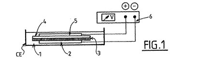
本発明の導電性機械的相互接続要素を製造する方法は、2つの段階を備える。図1に図式的に示される第1の段階は、国際公開2006/123049号に詳細に記載されている。 The method of manufacturing the conductive mechanical interconnection element of the present invention comprises two stages. The first stage, shown schematically in FIG. 1, is described in detail in WO 2006/123049.
第1の段階は次のステップを含む。 The first stage includes the following steps.
ステップi):金属材料の前駆物質である化合物の電解液1を電解セルCEに入れる。典型的には、溶液は1または複数種の金属塩の水溶液または有機溶液である。金属は、具体的には次のもの、即ち、Cu、Sn、Co、Fe、Pb、Ni、Cr、Au、Pd、Pt、Ag、Bi、Sb、Al、Si、およびLiから選択することができる。異なる金属の塩が使用されるとき、金属が合金中で結合できることを保証するために注意が必要である。具体的な例として、電解液は、CuSO4(100g/L(リットル))、(NaH4)2SO4(20g/L)、およびジエチレントリアミン(80g/L)の水溶液であってよい。 Step i): An electrolytic solution 1 of a compound that is a precursor of a metal material is placed in the electrolytic cell CE. Typically, the solution is an aqueous or organic solution of one or more metal salts. The metal is specifically selected from the following: Cu, Sn, Co, Fe, Pb, Ni, Cr, Au, Pd, Pt, Ag, Bi, Sb, Al, Si, and Li. it can. When different metal salts are used, care must be taken to ensure that the metals can bond in the alloy. As a specific example, electrolyte, CuSO 4 (100g / L (liter)), may be an aqueous solution of (NaH 4) 2 SO 4 ( 20g / L), and diethylene tri A amine (80 g / L) .
ステップii):伝導性基板2を前記溶液1に浸漬する。基板は、少なくとも一方の面が多孔質膜3で被覆され、この多孔質膜3は、直線状貫通孔の実質上規則的な配列を提示する。伝導性基板2は、「裸の」マイクロ電子チップ上の金属メッキ区域によって、または集積回路のトラックによって構成することができる。膜は、好ましくはアルミナから作られ、数百ナノメートルから数十マイクロメートルの範囲の厚さを提示し、107から1010の実質上円筒形の孔(109が好ましい値である)を提示し、孔は、実質上均一で50nmから500nmの範囲の直径を有し、規則的な六角形配列として分布する。このタイプの膜は、供給者Whatmanによって「Anodisc」の名称で販売されている。
Step ii): The
他の形態では、他の材料によって構成された膜が使用されてよい。最も重要な点は、それらの膜が直線状貫通孔の実質上規則的な配列を提示することである。現在の技術状態において、最良の結果はアルミナ膜を用いて得られる。他のセラミック材料、例えば、酸化チタンTiO2は、満足度が少なくなるにしても、許容可能な代替物を構成する。 In other forms, membranes composed of other materials may be used. The most important point is that these membranes present a substantially regular arrangement of linear through-holes. In the current state of the art, the best results are obtained with an alumina membrane. Other ceramic materials, for example, titanium oxide TiO 2 will, in satisfaction decreases, constitute an acceptable alternative.
ステップiii):前記または各々の多孔質膜に対向し、膜から間隔を空けて配置された電極5を提供する。例えば、電極は、透過性セルロースシート4によって膜3から間隔を空けて配置された銅板によって構成されていてよい。 Step iii): Providing the electrode 5 facing the or each porous membrane and spaced from the membrane. For example, the electrode may be constituted by a copper plate arranged at a distance from the membrane 3 by the permeable cellulose sheet 4.
ステップiv):前記基板2を発電機6の負の端子に接続してカソードを構成し、前記電極5を前記発電機6の正の端子に接続してアノードを構成し、これによって、前記金属材料を、前記膜内の孔を介して基板表面上に電解堆積させるようにする。堆積は、連続的または律動的に実行され得る。例えば、その方法を実現する1つの手順は、30分にわたって、1mA/cm2の電流を250ミリ秒印加することと、20mA/cm2の電流を50ミリ秒印加することとを含むシーケンスを提供する。
Step iv): The
ステップv):前記多孔質膜3を溶解する。例えば、80℃の水酸化ナトリウムの1モラー(M)溶液に30秒間浸漬し、続いてH2SO4(1M)およびCuSO4(1M)の水溶液中で10秒間洗浄する。 Step v): The porous membrane 3 is dissolved. For example, it is immersed in a 1 molar (M) solution of sodium hydroxide at 80 ° C. for 30 seconds, followed by washing in an aqueous solution of H 2 SO 4 (1M) and CuSO 4 (1M) for 10 seconds.
膜3の溶解はブラシ状の構造10を解放する。構造10は、前記基板2の表面から突出するサブミクロン直径の複数の金属ワイヤ(「ナノワイヤ」)2aによって構成される。ワイヤ2aは、膜内の孔の痕跡を構成する。膜の特性は、結果として、ナノワイヤの直径、密度、および長さを決定する。
Dissolution of the membrane 3 releases the brush-
本願発明者らは、市販されている異なる多孔質アルミナ膜を使用して、様々なテストを実行した。どのような状況のもとでも、本願発明者らは、この方法により得られた2つの構造を対向して配置した後に共に押圧することによっては、十分な強度の電気および機械的相互接続を達成することができなかった。 The inventors have performed various tests using different commercially available porous alumina membranes. Under any circumstance, the inventors have achieved sufficient strength electrical and mechanical interconnections by pressing the two structures obtained by this method together and then pressing them together. I couldn't.
意外なことに、本願発明者らは、制御された部分的溶解の追加ステップ(ステップvi))によって、ナノワイヤが前もって薄くされるならば、良好な電気および機械特性を提示する相互接続を得ることができることを観察した。この部分溶解ステップの後の、これら「ブラシ」のより大きくなった多孔率が、ナノワイヤのより良好な相互貫入を可能とし、従って、一方の構造が他方の構造へ押圧される2つの構造間で、より密接な接触を達成するように思われる。 Surprisingly, the inventors have obtained an interconnect that exhibits good electrical and mechanical properties if the nanowire is pre-thinned by an additional step of controlled partial dissolution (step vi)). We observed that The increased porosity of these “brushes” after this partial dissolution step allows for better interpenetration of nanowires, and therefore between two structures where one structure is pressed onto the other structure. Seems to achieve a closer contact.
この制御された溶解は、様々な方法により、特に電流または強制バイアスを用いて或いは用いることなく実行することができる。「無電解」と呼ばれる電流または強制バイアスを用いない方法は、図2に示されるように、単に構造10を溶液11に浸漬することによって実行される。溶液11は、ナノワイヤを構成する金属が、制御されたやり方で溶解されることを可能にする。溶液は、金属を酸化させなければならず、且つ、金属酸化の生産物を溶解できなければならない。例えば、溶液は、溶解されるべき金属よりも酸化力のある化合物と、酸との混合物であることができる。例えば、銅から作られるナノワイヤの場合、範囲0.01Mから1M(好ましくは0.1Mに等しい)の濃度のH2SO4と、範囲0.3Mから0.003M(好ましくは0.03M)の濃度のH2O2との混合物を使用することができる。
This controlled lysis can be carried out in various ways, in particular with or without current or forced bias. A method that does not use current or forced bias, referred to as “electroless,” is performed by simply immersing
例示する酸性溶液に代えて、塩基性溶液を使用してもよい。 Instead of the illustrated acidic solution, a basic solution may be used.
印加されるべきアノード電位または電流を要求する他の方法も、ナノワイヤの部分制御溶解を可能にする。これらの方法のうち、定電流、定電位、または実際に直流もしくは交流電位或いは電流を使用するパルスバイアスに言及することができる。そのような状況において、堆積ステップiv)で使用したのと同じ溶液1中で溶解を実行することができる。 Other methods that require an anodic potential or current to be applied also allow partial controlled dissolution of the nanowires. Among these methods, mention may be made of constant current, constant potential, or pulse bias that actually uses a direct or alternating potential or current. In such a situation, the lysis can be carried out in the same solution 1 used in the deposition step iv).
制御された部分的溶解ステップiv)の終わりに得られる相互接続要素は、典型的には、1平方センチメートル当たり107から1010のワイヤ数(wire・cm−2)(好ましくは109のオーダ)を提示する。これらワイヤは、概して範囲5nmから300nmの、好ましくは10nmから200nmの直径、ならびに、概して範囲200nmから200μmの、好ましくは範囲500nmから100μmの長さを提示する。一般的に、ワイヤの長さは膜の厚さよりも小さいか等しい。
The interconnect elements obtained at the end of the controlled partial dissolution step iv) are typically 10 7 to 10 10 wires per square centimeter (wire · cm −2 ) (preferably on the order of 10 9 ). Present. These wires present a diameter generally in the range 5 nm to 300 nm, preferably 10 nm to 200 nm, and a length generally in the
相互接続要素の多孔率(「ブラシ」の総容積に対する空の空間の容積の比として定義される)は、正確な測定が困難ではあるが、典型的には、0.5から0.9の範囲にあり、典型的には約0.75である。 The porosity of the interconnect element (defined as the ratio of the volume of the empty space to the total volume of the “brush”) is difficult to accurately measure, but is typically between 0.5 and 0.9 In range, typically about 0.75.
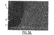
図3Aは、本発明の方法によって作られた相互接続要素12の電子顕微鏡観察図である。相互接続要素は銅基板2を備え、銅基板2はナノワイヤ2aを有する。ナノワイヤ2aは同じく銅から作られ、銅基板2の表面から突出する。これらナノワイヤは、約3μmの長さおよび約200nmの直径を提示する。ナノワイヤの密度Fは、約109/cm2である。
FIG. 3A is an electron microscopic view of an
図3Bは、図3Aに示されるタイプの2つの同じ相互接続要素12および12’を相互に押圧することによって作られた相互接続の電子顕微鏡観察図である。機械的接続に関与するナノワイヤ2aおよび2a’が、相互に貫入して絡み合っていることが分かるであろう。相互接続は50MPaの圧力を加えることによって行われ、要素12と12’との間に作用する結合力は、5N/cm2のオーダである。この相互接続は、明らかにナノワイヤを損傷することなく、単に牽引力を加えることによって切断され得る。結合力を著しく減少させることなく、相互接続の形成および切断の3つのサイクルを連続して実行することができる。
FIG. 3B is an electron microscopic view of an interconnect made by pressing together two
更に一般的には、相互接続を形成するために使用する圧力は、20MPaから100MPaの範囲にあり、結合力は3N/cm2から10N/cm2の範囲にある。 More generally, the pressure used to form the interconnect is in the range of 20 MPa to 100 MPa, and the bonding force is in the range of 3 N / cm 2 to 10 N / cm 2 .
本発明の相互接続要素は、フリップチップ電子アセンブリを作るために使用することができる。そのような状況において、チップおよび集積回路上の金属メッキ区域は、表面上にナノワイヤが電気化学的に堆積される基板として使用される。従来の電子アセンブリ手法と比較して、このタイプの相互接続の使用は、はんだ付け工程の間にチップが過熱される危険性を回避するのに役立つ。加えて、テスト、修理、または置換目的のために必要となり得るチップの取り外しが、かなり容易になる。 The interconnect elements of the present invention can be used to make flip chip electronic assemblies. In such a situation, the metal plated areas on the chip and integrated circuit are used as a substrate on which nanowires are electrochemically deposited on the surface. Compared to conventional electronic assembly techniques, the use of this type of interconnect helps to avoid the risk of the chip being overheated during the soldering process. In addition, chip removal, which may be required for testing, repair, or replacement purposes, is much easier.
好ましくは、相互接続要素は、こうして電気接続および機械接続の双方を提供し、ときには熱接続も提供する。しかしながら、これらの機能は別々であってもよい。 Preferably, the interconnection element thus provides both an electrical connection and a mechanical connection, and sometimes also provides a thermal connection. However, these functions may be separate.
本発明の特に有利な応用例は3次元集積にある。3次元集積は、例えばチップまたは小型プリント回路等の平面デバイスを積み重ねることから成る。従来技術で公知の1つの3次元集積手法が、欧州特許出願公開第0490739号明細書に記載されている。本発明の相互接続要素は、様々な平面デバイスの間に機械接続および電気接続の双方を提供することによって、そのような3次元デバイスの製作を簡易化することができる。このようにして製造された3次元デバイスは、分解可能であるという重要な利点を提示する。この利点は、従来技術の手法を使用するときには、ほとんど想像できない。 A particularly advantageous application of the invention is in three-dimensional integration. Three-dimensional integration consists of stacking planar devices such as chips or small printed circuits. One three-dimensional integration technique known in the prior art is described in EP 0 490 739. The interconnect elements of the present invention can simplify the fabrication of such three-dimensional devices by providing both mechanical and electrical connections between various planar devices. A three-dimensional device manufactured in this way presents the important advantage of being decomposable. This advantage is almost unimaginable when using prior art approaches.
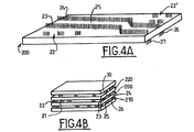
3次元集積は、熱放散の厳しい問題を提起する。本発明の相互接続要素は、図4Aおよび図4Bで示されるように、この問題に対して独創的な解決法を提供し得る。 Three-dimensional integration raises the severe problem of heat dissipation. The interconnect element of the present invention may provide an ingenious solution to this problem, as shown in FIGS. 4A and 4B.
図4Aに、集積回路の3次元スタックの一部分を形成するマイクロ電子チップ200を示す。参照番号21で示されるその上面および下面(図示されず)は、金属メッキ区域を基板として使用して、本発明の方法によって作られた相互接続要素を保有している。実質的に正方形形状の相互接続要素22および22’の2つのグループが見られる。これら相互接続要素は、電気信号を通すのに役立ち、チップ200とその上下に置かれるべき他のチップ(図4Bの参照番号210および220)との間で、機械的結合を形成するのに貢献する。相互接続要素23および24は、直線状ストリップである必要はなく、チップ200を一方の側から他方の側へ横断する並列ストリップの形態をしている。これら相互接続要素はチップから電気的に絶縁されている(相互接続要素の基板は、例えば、SiO2から作られた絶縁層上に形成された金属メッキによって構成される)。同様に、ストリップ23と24との間にあるチップ表面領域25は、不動態化されている。チップの底面は、並列ストリップ26および27の形態をした相互接続要素を同様に提示することが、図中で見られ得る。
FIG. 4A shows a
対応する相互接続要素を提示する同じタイプの複数のチップが積み重ねられて相互に押圧される場合は、図4Bで示されるタイプの3次元構造が得られる。 If multiple chips of the same type presenting corresponding interconnect elements are stacked and pressed together, a three-dimensional structure of the type shown in FIG. 4B is obtained.
図4Bに、ストリップ23および24の形態をした導体要素およびそれらのストリップ間に画定された領域25が、隣接するチップ210の対応部分と協同して、チャネルまたは管30を形成することを示す。相互接続要素23および24は、漏れのない壁を形成する。その結果、構造の電子回路によって放散された熱を除去するために、このチャネル(および、様々なチップ間のインタフェースで形成されたチャネルの全て)において冷却流体が流れるようにすることができる。
FIG. 4B shows that conductor elements in the form of
Claims (30)
i)金属材料の前駆物質である化合物の電解液(1)を電解セル(CE)に入れるステップと、
ii)直線状貫通孔の実質的に規則的な配列を提示する多孔質膜(3)で被覆された少なくとも1つの面を有する伝導性基板(2)を、前記電解液中に浸漬するステップと、
iii)前記または各々の多孔質膜に対向し、前記多孔質膜から間隔を空けて配置された電極(5)を提供するステップと、
iv)前記基板を発電機(6)の負の端子へ接続してカソードを構成し、前記電極を前記発電機の正の端子へ接続してアノードを構成し、前記膜の前記孔を介して前記基板の表面上で前記金属材料の電解堆積を実行するステップと、
v)前記多孔質膜を溶解して、前記金属材料から作られて前記基板(2)の表面から突出するサブミクロン直径の複数のワイヤ(2a)を備える構造(10)を解放するステップと、から成る段階を含み、
vi)2つの前記構造の一方が他方へ押圧された場合に、前記ワイヤが相互に貫入および絡み合う結果として、2つの前記構造間で作用する接着力が増加するように、前記ワイヤ(2a)の部分的溶解を制御して前記ワイヤの直径を低減する追加のステップを更に含むことを特徴とする方法。 A method of manufacturing a conductive mechanical interconnect element (12) comprising:
i) placing an electrolytic solution (1) of a compound that is a precursor of a metal material into an electrolytic cell (CE);
ii) immersing a conductive substrate (2) having at least one surface coated with a porous membrane (3) presenting a substantially regular arrangement of linear through-holes in said electrolyte solution; ,
iii) providing an electrode (5) opposite the or each porous membrane and spaced from the porous membrane;
iv) Connect the substrate to the negative terminal of the generator (6) to form a cathode, connect the electrode to the positive terminal of the generator to form an anode, and through the holes in the membrane Performing electrolytic deposition of the metallic material on the surface of the substrate;
v) dissolving the porous membrane to release a structure (10) comprising a plurality of submicron diameter wires (2a) made from the metallic material and projecting from the surface of the substrate (2); Comprising the steps of:
vi) When one of the two structures is pressed against the other, the wire (2a) of the wire (2a) is increased so that the adhesive force acting between the two structures increases as a result of the wires penetrating and entangled with each other. The method further comprising the additional step of controlling partial dissolution to reduce the diameter of the wire.
請求項1〜17のいずれかに記載の方法によって、2つの相互接続要素(12、12’)を製造することと、
前記要素の表面から突出する前記ナノメトリックワイヤが相互に貫入および絡み合うようにするために、前記相互接続要素を対向させて配置して、一方の前記要素を他方の前記要素へ押圧することと、
から成るステップを含む方法。 A method of making a mechanical interconnect,
Producing two interconnecting elements (12, 12 ') by the method according to any of claims 1 to 17 ,
Placing the interconnect elements facing each other and pressing one element against the other element so that the nanometric wires projecting from the surface of the element penetrate and intertwine with each other;
A method comprising a step consisting of:
Applications Claiming Priority (3)
| Application Number | Priority Date | Filing Date | Title |
|---|---|---|---|
| FR0707566A FR2923078B1 (en) | 2007-10-26 | 2007-10-26 | METHOD FOR MANUFACTURING ELECTRICALLY CONDUCTIVE MECHANICAL INTERCONNECTION MEMBER |
| FR0707566 | 2007-10-26 | ||
| PCT/FR2008/001497 WO2009090349A2 (en) | 2007-10-26 | 2008-10-24 | Method for making an electrically conducting mechanical interconnection member |
Publications (2)
| Publication Number | Publication Date |
|---|---|
| JP2011501454A JP2011501454A (en) | 2011-01-06 |
| JP5374512B2 true JP5374512B2 (en) | 2013-12-25 |
Family
ID=39456439
Family Applications (1)
| Application Number | Title | Priority Date | Filing Date |
|---|---|---|---|
| JP2010530510A Expired - Fee Related JP5374512B2 (en) | 2007-10-26 | 2008-10-24 | Method for making conductive mechanical interconnect members |
Country Status (5)
| Country | Link |
|---|---|
| US (1) | US8178416B2 (en) |
| EP (1) | EP2218102B1 (en) |
| JP (1) | JP5374512B2 (en) |
| FR (1) | FR2923078B1 (en) |
| WO (1) | WO2009090349A2 (en) |
Families Citing this family (8)
| Publication number | Priority date | Publication date | Assignee | Title |
|---|---|---|---|---|
| DE102009059304B4 (en) | 2009-12-23 | 2014-07-03 | CiS Forschungsinstitut für Mikrosensorik und Photovoltaik GmbH | Silicon chip with a cable attached to it and procedures for attaching the cable |
| US8916959B2 (en) | 2012-12-20 | 2014-12-23 | International Business Machines Corporation | Packaging structure |
| EP2871675A1 (en) * | 2013-11-06 | 2015-05-13 | Mitsubishi Electric R & D Centre Europe B.V. | Pressure connection for a semiconductor die using flexible nanowires and corresponding manufacturing method |
| US9583410B2 (en) | 2014-03-21 | 2017-02-28 | International Business Machines Corporation | Volumetric integrated circuit and volumetric integrated circuit manufacturing method |
| WO2018145968A1 (en) * | 2017-02-09 | 2018-08-16 | Siemens Aktiengesellschaft | Power module |
| DE102017104902A1 (en) | 2017-03-08 | 2018-09-13 | Olav Birlem | Arrangement of semiconductor chips and method for the production thereof |
| DE102020107515A1 (en) * | 2020-03-18 | 2021-09-23 | Nanowired Gmbh | Multimetal Velcro Welding |
| CN118431184A (en) * | 2024-07-05 | 2024-08-02 | 芯梦达半导体科技(济南)有限公司 | Storage device, semiconductor device and memory system |
Family Cites Families (20)
| Publication number | Priority date | Publication date | Assignee | Title |
|---|---|---|---|---|
| US5877069A (en) * | 1996-09-16 | 1999-03-02 | Micron Technology, Inc. | Method for electrochemical local oxidation of silicon |
| CA2286326C (en) * | 1997-04-04 | 2007-06-26 | Adam L. Cohen | Article, method, and apparatus for electrochemical fabrication |
| US6231744B1 (en) * | 1997-04-24 | 2001-05-15 | Massachusetts Institute Of Technology | Process for fabricating an array of nanowires |
| DE59909242D1 (en) * | 1998-03-10 | 2004-05-27 | Micronas Gmbh | REFERENCE ELECTRODE |
| US6417069B1 (en) * | 1999-03-25 | 2002-07-09 | Canon Kabushiki Kaisha | Substrate processing method and manufacturing method, and anodizing apparatus |
| JP4547728B2 (en) * | 1999-03-29 | 2010-09-22 | ソニー株式会社 | Semiconductor device and manufacturing method thereof |
| JP3445187B2 (en) * | 1999-08-03 | 2003-09-08 | キヤノン株式会社 | Semiconductor device defect compensation method |
| US6741019B1 (en) * | 1999-10-18 | 2004-05-25 | Agere Systems, Inc. | Article comprising aligned nanowires |
| AT408052B (en) * | 1999-11-10 | 2001-08-27 | Electrovac | CONNECTION SYSTEM |
| JP2004502554A (en) * | 2000-03-22 | 2004-01-29 | ユニバーシティー オブ マサチューセッツ | Nano cylinder array |
| EP1320111A1 (en) * | 2001-12-11 | 2003-06-18 | Abb Research Ltd. | Carbon nanotube contact for MEMS |
| JP2004353061A (en) * | 2003-05-30 | 2004-12-16 | Ebara Corp | Electrolytic treatment method and apparatus |
| US7327037B2 (en) * | 2004-04-01 | 2008-02-05 | Lucent Technologies Inc. | High density nanostructured interconnection |
| US7129567B2 (en) * | 2004-08-31 | 2006-10-31 | Micron Technology, Inc. | Substrate, semiconductor die, multichip module, and system including a via structure comprising a plurality of conductive elements |
| WO2006098026A1 (en) * | 2005-03-17 | 2006-09-21 | Fujitsu Limited | Connecting mechanism, semiconductor package and method for manufacturing such semiconductor package |
| FR2885913B1 (en) * | 2005-05-18 | 2007-08-10 | Centre Nat Rech Scient | COMPOSITE ELEMENT COMPRISING A CONDUCTIVE SUBSTRATE AND A NANOSTRUCTURED METAL COATING. |
| US7371674B2 (en) * | 2005-12-22 | 2008-05-13 | Intel Corporation | Nanostructure-based package interconnect |
| US7967967B2 (en) * | 2007-01-16 | 2011-06-28 | Tesla Laboratories, LLC | Apparatus and method for electrochemical modification of liquid streams |
| JP5358303B2 (en) * | 2008-06-30 | 2013-12-04 | クロリンエンジニアズ株式会社 | Method of cleaning with electrolytic sulfuric acid and method of manufacturing semiconductor device |
| JP5320173B2 (en) * | 2008-06-30 | 2013-10-23 | クロリンエンジニアズ株式会社 | Sulfuric acid electrolysis method |
-
2007
- 2007-10-26 FR FR0707566A patent/FR2923078B1/en active Active
-
2008
- 2008-10-24 JP JP2010530510A patent/JP5374512B2/en not_active Expired - Fee Related
- 2008-10-24 WO PCT/FR2008/001497 patent/WO2009090349A2/en not_active Ceased
- 2008-10-24 EP EP08870576.9A patent/EP2218102B1/en not_active Not-in-force
- 2008-10-24 US US12/739,848 patent/US8178416B2/en not_active Expired - Fee Related
Also Published As
| Publication number | Publication date |
|---|---|
| EP2218102A2 (en) | 2010-08-18 |
| US20100308473A1 (en) | 2010-12-09 |
| WO2009090349A2 (en) | 2009-07-23 |
| JP2011501454A (en) | 2011-01-06 |
| FR2923078B1 (en) | 2017-09-01 |
| EP2218102B1 (en) | 2016-02-10 |
| WO2009090349A3 (en) | 2009-09-17 |
| US8178416B2 (en) | 2012-05-15 |
| FR2923078A1 (en) | 2009-05-01 |
Similar Documents
| Publication | Publication Date | Title |
|---|---|---|
| JP5374512B2 (en) | Method for making conductive mechanical interconnect members | |
| KR101496494B1 (en) | Method for manufacturing anisotropic conductive joint package | |
| US20110043239A1 (en) | Probe card | |
| TWI429581B (en) | Nano carbon tube contact structure | |
| JP5143045B2 (en) | Fine structure and manufacturing method thereof | |
| TW201706131A (en) | Thermal interface material using metal nanowire array and sacrificial template | |
| TWI862805B (en) | Anodic oxide structure and probe head comprising thereof and probe card comprising thereof | |
| TW201030913A (en) | Manufacturing method for semiconductor devices | |
| US11800602B1 (en) | Multilayered metal nanowire array | |
| US7891090B2 (en) | Method for manufacturing an interposer | |
| TWI850627B (en) | Composite mold, metal product and method for manufacturing the product | |
| US20130162280A1 (en) | Probe card and method of manufacturing the same | |
| JP5824435B2 (en) | Anisotropic conductive member and multilayer wiring board | |
| JP2009244244A (en) | Probe card | |
| TW202140863A (en) | Anodic oxidation film mold, probe half finished product, probe card and manufacturing methods thereof | |
| Luan et al. | Nano copper wires interconnection for three—dimensional integration in power electronics | |
| TW202240176A (en) | The electro-conductive contact pin and manufacturing method thereof | |
| TW202303159A (en) | Electro-conductive contact pin and manufacturing method thereof | |
| Tunaboylu | Performance of Ni-alloy MEMS-probes coated with PdCo films in semiconductor wafer test | |
| TW202323828A (en) | The cantilever probe pin | |
| CN121762888A (en) | Electroplated metal layer of MEMS probe | |
| CN120547776A (en) | Method for manufacturing micro-pitch circuit board, micro-pitch circuit board and LED device | |
| JP2011070828A (en) | Conductive substrate, conductive substrate assembly, and manufacturing method of conductive substrate | |
| JP2009047565A (en) | Sheet probe and manufacturing method thereof | |
| Razeeb et al. | 3D interconnection by FIB assisted Pt deposition and electroless nickel deposition on the sides and edges of an I-Seed |
Legal Events
| Date | Code | Title | Description |
|---|---|---|---|
| A621 | Written request for application examination |
Free format text: JAPANESE INTERMEDIATE CODE: A621 Effective date: 20111006 |
|
| A977 | Report on retrieval |
Free format text: JAPANESE INTERMEDIATE CODE: A971007 Effective date: 20130227 |
|
| A131 | Notification of reasons for refusal |
Free format text: JAPANESE INTERMEDIATE CODE: A131 Effective date: 20130312 |
|
| A601 | Written request for extension of time |
Free format text: JAPANESE INTERMEDIATE CODE: A601 Effective date: 20130607 |
|
| A602 | Written permission of extension of time |
Free format text: JAPANESE INTERMEDIATE CODE: A602 Effective date: 20130614 |
|
| A521 | Request for written amendment filed |
Free format text: JAPANESE INTERMEDIATE CODE: A523 Effective date: 20130806 |
|
| TRDD | Decision of grant or rejection written | ||
| A01 | Written decision to grant a patent or to grant a registration (utility model) |
Free format text: JAPANESE INTERMEDIATE CODE: A01 Effective date: 20130827 |
|
| A61 | First payment of annual fees (during grant procedure) |
Free format text: JAPANESE INTERMEDIATE CODE: A61 Effective date: 20130920 |
|
| R150 | Certificate of patent or registration of utility model |
Ref document number: 5374512 Country of ref document: JP Free format text: JAPANESE INTERMEDIATE CODE: R150 Free format text: JAPANESE INTERMEDIATE CODE: R150 |
|
| R250 | Receipt of annual fees |
Free format text: JAPANESE INTERMEDIATE CODE: R250 |
|
| R250 | Receipt of annual fees |
Free format text: JAPANESE INTERMEDIATE CODE: R250 |
|
| R250 | Receipt of annual fees |
Free format text: JAPANESE INTERMEDIATE CODE: R250 |
|
| LAPS | Cancellation because of no payment of annual fees |