JP5374706B2 - 電波吸収体の実効厚み制御法 - Google Patents
電波吸収体の実効厚み制御法 Download PDFInfo
- Publication number
- JP5374706B2 JP5374706B2 JP2010171472A JP2010171472A JP5374706B2 JP 5374706 B2 JP5374706 B2 JP 5374706B2 JP 2010171472 A JP2010171472 A JP 2010171472A JP 2010171472 A JP2010171472 A JP 2010171472A JP 5374706 B2 JP5374706 B2 JP 5374706B2
- Authority
- JP
- Japan
- Prior art keywords
- radio wave
- wave absorber
- thickness
- electromagnetic wave
- absorber
- Prior art date
- Legal status (The legal status is an assumption and is not a legal conclusion. Google has not performed a legal analysis and makes no representation as to the accuracy of the status listed.)
- Active
Links
- 239000006096 absorbing agent Substances 0.000 title claims abstract description 115
- 238000000034 method Methods 0.000 title claims abstract description 17
- 238000010521 absorption reaction Methods 0.000 claims description 35
- 239000000463 material Substances 0.000 claims description 18
- 238000010030 laminating Methods 0.000 claims description 2
- 238000004519 manufacturing process Methods 0.000 abstract description 11
- 238000013461 design Methods 0.000 abstract description 4
- 239000010410 layer Substances 0.000 description 15
- 239000002356 single layer Substances 0.000 description 7
- 239000011230 binding agent Substances 0.000 description 5
- OKTJSMMVPCPJKN-UHFFFAOYSA-N Carbon Chemical compound [C] OKTJSMMVPCPJKN-UHFFFAOYSA-N 0.000 description 3
- 238000005259 measurement Methods 0.000 description 3
- 229920005989 resin Polymers 0.000 description 3
- 239000011347 resin Substances 0.000 description 3
- 238000012360 testing method Methods 0.000 description 3
- 229910000859 α-Fe Inorganic materials 0.000 description 3
- XEEYBQQBJWHFJM-UHFFFAOYSA-N Iron Chemical compound [Fe] XEEYBQQBJWHFJM-UHFFFAOYSA-N 0.000 description 2
- 230000002950 deficient Effects 0.000 description 2
- 230000000694 effects Effects 0.000 description 2
- 229920001971 elastomer Polymers 0.000 description 2
- 239000003973 paint Substances 0.000 description 2
- 230000035699 permeability Effects 0.000 description 2
- 239000000843 powder Substances 0.000 description 2
- 230000002265 prevention Effects 0.000 description 2
- 238000002310 reflectometry Methods 0.000 description 2
- 238000012935 Averaging Methods 0.000 description 1
- 101000912561 Bos taurus Fibrinogen gamma-B chain Proteins 0.000 description 1
- 239000004593 Epoxy Substances 0.000 description 1
- 229910052799 carbon Inorganic materials 0.000 description 1
- 239000006229 carbon black Substances 0.000 description 1
- 239000011203 carbon fibre reinforced carbon Substances 0.000 description 1
- 239000002041 carbon nanotube Substances 0.000 description 1
- 229910021393 carbon nanotube Inorganic materials 0.000 description 1
- 230000015556 catabolic process Effects 0.000 description 1
- 238000006243 chemical reaction Methods 0.000 description 1
- 239000011248 coating agent Substances 0.000 description 1
- 238000000576 coating method Methods 0.000 description 1
- 239000004020 conductor Substances 0.000 description 1
- 238000006731 degradation reaction Methods 0.000 description 1
- 230000007257 malfunction Effects 0.000 description 1
- 239000002184 metal Substances 0.000 description 1
- 229910052751 metal Inorganic materials 0.000 description 1
- 238000012986 modification Methods 0.000 description 1
- 230000004048 modification Effects 0.000 description 1
- 238000012545 processing Methods 0.000 description 1
- 230000005855 radiation Effects 0.000 description 1
- 239000000126 substance Substances 0.000 description 1
- 230000001629 suppression Effects 0.000 description 1
- 229920002803 thermoplastic polyurethane Polymers 0.000 description 1
- 239000002699 waste material Substances 0.000 description 1
Images


Landscapes
- Shielding Devices Or Components To Electric Or Magnetic Fields (AREA)
Description
S[dB]=−20log10|Γ| (1)
Γ=(Zin−1)/(Zin+1) (2)
一般的に電波吸収体の性能としては、所望の運用周波数帯域で電波吸収量として20dB以上が必要とされているため、以下の式(4)が設計条件となる。
|Γ|≦0.1 (4)
(但し、前記N個の電波吸収部材のうち、少なくとも一つは、厚みd n が異なるものとする)
に従って面状に配置することにより、面積Sで厚みdの電波吸収体と実質的に等価な電波吸収特性とすることを特徴としている。
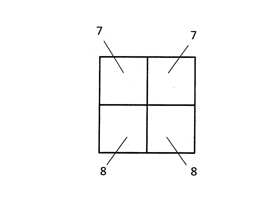
この場合、各電波吸収部材の面積は同一でも異なっていてもよいが、電波器材の放射ビーム径内に上記電波吸収体(面状配置の電波吸収部材群)が収まるように、個々の電波吸収部材の面積を小さくすることが必要である。
なお、Γは電気定数及び厚みの関数であるが、個々の電波吸収部材は同一材料なのでここでは電気定数の表示を省略し、厚みdnのみの関数として表示した。(5)式で定義される厚みをdeffとしてΔdn=dn−deffとおくと、ΓtはΔdnがdnよりも十分小さいとして以下のように近似される。
ここで、(8)式中、Γ′はΓのdnに関する微分係数である。実際の電波吸収体に使用される電気定数及び厚みを用いて(8)式を計算すると、その第2項は第1項に対して殆ど無視できることが確認できる。従って、Γtは実質的にΓ(deff)に等しく、すなわち前記N個の電波吸収部材を配置した電波吸収体は厚みdeffの電波吸収体と同じ吸収性能を有することがわかる。従って前記N個の電波吸収部材からなる電波吸収体の実効厚みはdeffであると言える。
2 電波吸収層
3〜6 電気定数が同一の電波吸収部材
7 第1の電波吸収部材
8 第2の電波吸収部材
Claims (3)
- 同一材料で一様な厚みd n 、面積S n を有するN個の電波吸収部材を、下記条件式(5),(6)
(但し、前記N個の電波吸収部材のうち、少なくとも一つは、厚みd n が異なるものとする)
に従って面状に配置することにより、面積Sで厚みdの電波吸収体と実質的に等価な電波吸収特性とすることを特徴とする電波吸収体の実効厚み制御法。 - 前記N個の電波吸収部材のうち、少なくとも一つは面積S n を異ならせた、請求項1記載の電波吸収体の実効厚み制御法。
- 前記N個の電波吸収部材は電波反射層上に一様な厚みの電波吸収層を積層したものである、請求項1又は2記載の電波吸収体の実効厚み制御法。
Priority Applications (1)
| Application Number | Priority Date | Filing Date | Title |
|---|---|---|---|
| JP2010171472A JP5374706B2 (ja) | 2010-07-30 | 2010-07-30 | 電波吸収体の実効厚み制御法 |
Applications Claiming Priority (1)
| Application Number | Priority Date | Filing Date | Title |
|---|---|---|---|
| JP2010171472A JP5374706B2 (ja) | 2010-07-30 | 2010-07-30 | 電波吸収体の実効厚み制御法 |
Publications (2)
| Publication Number | Publication Date |
|---|---|
| JP2012033675A JP2012033675A (ja) | 2012-02-16 |
| JP5374706B2 true JP5374706B2 (ja) | 2013-12-25 |
Family
ID=45846749
Family Applications (1)
| Application Number | Title | Priority Date | Filing Date |
|---|---|---|---|
| JP2010171472A Active JP5374706B2 (ja) | 2010-07-30 | 2010-07-30 | 電波吸収体の実効厚み制御法 |
Country Status (1)
| Country | Link |
|---|---|
| JP (1) | JP5374706B2 (ja) |
Families Citing this family (1)
| Publication number | Priority date | Publication date | Assignee | Title |
|---|---|---|---|---|
| US11828870B2 (en) * | 2018-09-21 | 2023-11-28 | Honda Motor Co., Ltd. | Vehicle inspection system |
Family Cites Families (7)
| Publication number | Priority date | Publication date | Assignee | Title |
|---|---|---|---|---|
| JPS52131200A (en) * | 1976-04-26 | 1977-11-02 | Nippon Telegr & Teleph Corp <Ntt> | Electric wave absorber |
| JPS5927597A (ja) * | 1982-08-06 | 1984-02-14 | ティーディーケイ株式会社 | 電波吸収体 |
| JPH0638475Y2 (ja) * | 1990-11-29 | 1994-10-05 | 日立フェライト株式会社 | 電波吸収壁 |
| JPH057093A (ja) * | 1991-06-28 | 1993-01-14 | Osaka Gas Co Ltd | 電波吸収体 |
| JP2000165081A (ja) * | 1998-11-25 | 2000-06-16 | Nec Miyagi Ltd | 広帯域電波吸収体 |
| JP2002009483A (ja) * | 2000-06-26 | 2002-01-11 | Kitagawa Ind Co Ltd | 電波吸収体 |
| JP4476734B2 (ja) * | 2004-07-30 | 2010-06-09 | 株式会社熊谷組 | 内装構造及び内装施工方法 |
-
2010
- 2010-07-30 JP JP2010171472A patent/JP5374706B2/ja active Active
Also Published As
| Publication number | Publication date |
|---|---|
| JP2012033675A (ja) | 2012-02-16 |
Similar Documents
| Publication | Publication Date | Title |
|---|---|---|
| He et al. | Multisection step-impedance modeling and analysis of broadband microwave honeycomb absorbing structures | |
| Chen et al. | Flexible and conformable broadband metamaterial absorber with wide-angle and polarization stability for radar application | |
| Duan et al. | Design and preparation of an ultrathin broadband metamaterial absorber with a magnetic substrate based on genetic algorithm | |
| JP5047195B2 (ja) | エンブレム | |
| US20080165442A1 (en) | System, method and apparatus for cloaking | |
| Koduru et al. | Transducer arrays for omnidirectional guided wave mode control in plate like structures | |
| US20130017348A1 (en) | Invisible enclosure | |
| CN104103898B (zh) | 高透波低rcs天线罩 | |
| JP4944044B2 (ja) | 集積アンテナのレーダ断面積を減少する方法及び構成 | |
| Abu Sanad et al. | Theory, modeling, measurement, and testing of electromagnetic absorbers: A review | |
| WO2002043460A1 (fr) | Absorbeur d'ondes radioelectriques | |
| Wang et al. | Double‐layer structural compatible protective material with excellent microwave absorption and heat shielding performance | |
| JP5654249B2 (ja) | 積層型木質系電波吸収板材及びその作製方法 | |
| Rani et al. | Utilization of graphene oxide-based microwave absorber for pattern enhancement of patch antenna array | |
| JP5224529B2 (ja) | 不可視包囲体 | |
| JP2012033675A (ja) | 電波吸収体の実効厚み制御法及び電波吸収体 | |
| Pratap et al. | Structural design of radar absorber using glass fiber-epoxy composites loaded with BaU hexaferrite for defence applications | |
| JP5493132B2 (ja) | 電波吸収体及びその設計方法 | |
| Xie et al. | Design and development of conformal antenna composite structure | |
| Li et al. | Suppressing edge back-scattering of electromagnetic waves using coding metasurface purfle | |
| WO2022009960A1 (ja) | 樹脂成形体及びその製造方法 | |
| CN113394561A (zh) | 用于多波段合成孔径雷达天线的超宽带天线罩及测试方法 | |
| Vovchenko et al. | Optimization of multilayered electromagnetic shielding using mesh adaptive direct search | |
| KR101004026B1 (ko) | 광대역 2층형 전자파 흡수체 시트 및 이를 제조하는 방법 | |
| CN102770008A (zh) | 一种吸波装置 |
Legal Events
| Date | Code | Title | Description |
|---|---|---|---|
| A131 | Notification of reasons for refusal |
Free format text: JAPANESE INTERMEDIATE CODE: A131 Effective date: 20120314 |
|
| A131 | Notification of reasons for refusal |
Free format text: JAPANESE INTERMEDIATE CODE: A131 Effective date: 20121205 |
|
| A521 | Written amendment |
Free format text: JAPANESE INTERMEDIATE CODE: A523 Effective date: 20130131 |
|
| TRDD | Decision of grant or rejection written | ||
| A01 | Written decision to grant a patent or to grant a registration (utility model) |
Free format text: JAPANESE INTERMEDIATE CODE: A01 Effective date: 20130821 |
|
| R150 | Certificate of patent or registration of utility model |
Free format text: JAPANESE INTERMEDIATE CODE: R150 |
|
| S533 | Written request for registration of change of name |
Free format text: JAPANESE INTERMEDIATE CODE: R313533 |
|
| R350 | Written notification of registration of transfer |
Free format text: JAPANESE INTERMEDIATE CODE: R350 |