JP5374831B2 - 複数の半導体チップおよび電子部品を備える2枚の基板を有するパワーエレクトロニックパッケージ - Google Patents
複数の半導体チップおよび電子部品を備える2枚の基板を有するパワーエレクトロニックパッケージ Download PDFInfo
- Publication number
- JP5374831B2 JP5374831B2 JP2007126042A JP2007126042A JP5374831B2 JP 5374831 B2 JP5374831 B2 JP 5374831B2 JP 2007126042 A JP2007126042 A JP 2007126042A JP 2007126042 A JP2007126042 A JP 2007126042A JP 5374831 B2 JP5374831 B2 JP 5374831B2
- Authority
- JP
- Japan
- Prior art keywords
- thermal conductivity
- high thermal
- power electronic
- electronic package
- conductivity insulating
- Prior art date
- Legal status (The legal status is an assumption and is not a legal conclusion. Google has not performed a legal analysis and makes no representation as to the accuracy of the status listed.)
- Expired - Fee Related
Links
Images



















Classifications
-
- H—ELECTRICITY
- H10—SEMICONDUCTOR DEVICES; ELECTRIC SOLID-STATE DEVICES NOT OTHERWISE PROVIDED FOR
- H10W—GENERIC PACKAGES, INTERCONNECTIONS, CONNECTORS OR OTHER CONSTRUCTIONAL DETAILS OF DEVICES COVERED BY CLASS H10
- H10W70/00—Package substrates; Interposers; Redistribution layers [RDL]
- H10W70/60—Insulating or insulated package substrates; Interposers; Redistribution layers
- H10W70/62—Insulating or insulated package substrates; Interposers; Redistribution layers characterised by their interconnections
- H10W70/65—Shapes or dispositions of interconnections
- H10W70/658—Shapes or dispositions of interconnections for devices provided for in groups H10D8/00 - H10D48/00
-
- H—ELECTRICITY
- H10—SEMICONDUCTOR DEVICES; ELECTRIC SOLID-STATE DEVICES NOT OTHERWISE PROVIDED FOR
- H10W—GENERIC PACKAGES, INTERCONNECTIONS, CONNECTORS OR OTHER CONSTRUCTIONAL DETAILS OF DEVICES COVERED BY CLASS H10
- H10W70/00—Package substrates; Interposers; Redistribution layers [RDL]
- H10W70/60—Insulating or insulated package substrates; Interposers; Redistribution layers
- H10W70/611—Insulating or insulated package substrates; Interposers; Redistribution layers for connecting multiple chips together
-
- H—ELECTRICITY
- H10—SEMICONDUCTOR DEVICES; ELECTRIC SOLID-STATE DEVICES NOT OTHERWISE PROVIDED FOR
- H10W—GENERIC PACKAGES, INTERCONNECTIONS, CONNECTORS OR OTHER CONSTRUCTIONAL DETAILS OF DEVICES COVERED BY CLASS H10
- H10W90/00—Package configurations
-
- H—ELECTRICITY
- H10—SEMICONDUCTOR DEVICES; ELECTRIC SOLID-STATE DEVICES NOT OTHERWISE PROVIDED FOR
- H10W—GENERIC PACKAGES, INTERCONNECTIONS, CONNECTORS OR OTHER CONSTRUCTIONAL DETAILS OF DEVICES COVERED BY CLASS H10
- H10W90/00—Package configurations
- H10W90/401—Package configurations characterised by multiple insulating or insulated package substrates, interposers or RDLs
-
- H—ELECTRICITY
- H10—SEMICONDUCTOR DEVICES; ELECTRIC SOLID-STATE DEVICES NOT OTHERWISE PROVIDED FOR
- H10W—GENERIC PACKAGES, INTERCONNECTIONS, CONNECTORS OR OTHER CONSTRUCTIONAL DETAILS OF DEVICES COVERED BY CLASS H10
- H10W40/00—Arrangements for thermal protection or thermal control
- H10W40/20—Arrangements for cooling
- H10W40/25—Arrangements for cooling characterised by their materials
- H10W40/255—Arrangements for cooling characterised by their materials having a laminate or multilayered structure, e.g. direct bond copper [DBC] ceramic substrates
-
- H—ELECTRICITY
- H10—SEMICONDUCTOR DEVICES; ELECTRIC SOLID-STATE DEVICES NOT OTHERWISE PROVIDED FOR
- H10W—GENERIC PACKAGES, INTERCONNECTIONS, CONNECTORS OR OTHER CONSTRUCTIONAL DETAILS OF DEVICES COVERED BY CLASS H10
- H10W72/00—Interconnections or connectors in packages
- H10W72/071—Connecting or disconnecting
- H10W72/073—Connecting or disconnecting of die-attach connectors
- H10W72/07331—Connecting techniques
-
- H—ELECTRICITY
- H10—SEMICONDUCTOR DEVICES; ELECTRIC SOLID-STATE DEVICES NOT OTHERWISE PROVIDED FOR
- H10W—GENERIC PACKAGES, INTERCONNECTIONS, CONNECTORS OR OTHER CONSTRUCTIONAL DETAILS OF DEVICES COVERED BY CLASS H10
- H10W72/00—Interconnections or connectors in packages
- H10W72/071—Connecting or disconnecting
- H10W72/073—Connecting or disconnecting of die-attach connectors
- H10W72/07331—Connecting techniques
- H10W72/07336—Soldering or alloying
-
- H—ELECTRICITY
- H10—SEMICONDUCTOR DEVICES; ELECTRIC SOLID-STATE DEVICES NOT OTHERWISE PROVIDED FOR
- H10W—GENERIC PACKAGES, INTERCONNECTIONS, CONNECTORS OR OTHER CONSTRUCTIONAL DETAILS OF DEVICES COVERED BY CLASS H10
- H10W72/00—Interconnections or connectors in packages
- H10W72/071—Connecting or disconnecting
- H10W72/073—Connecting or disconnecting of die-attach connectors
- H10W72/07351—Connecting or disconnecting of die-attach connectors characterised by changes in properties of the die-attach connectors during connecting
-
- H—ELECTRICITY
- H10—SEMICONDUCTOR DEVICES; ELECTRIC SOLID-STATE DEVICES NOT OTHERWISE PROVIDED FOR
- H10W—GENERIC PACKAGES, INTERCONNECTIONS, CONNECTORS OR OTHER CONSTRUCTIONAL DETAILS OF DEVICES COVERED BY CLASS H10
- H10W72/00—Interconnections or connectors in packages
- H10W72/30—Die-attach connectors
-
- H—ELECTRICITY
- H10—SEMICONDUCTOR DEVICES; ELECTRIC SOLID-STATE DEVICES NOT OTHERWISE PROVIDED FOR
- H10W—GENERIC PACKAGES, INTERCONNECTIONS, CONNECTORS OR OTHER CONSTRUCTIONAL DETAILS OF DEVICES COVERED BY CLASS H10
- H10W80/00—Direct bonding of chips, wafers or substrates
- H10W80/301—Bonding techniques, e.g. hybrid bonding
Landscapes
- Cooling Or The Like Of Semiconductors Or Solid State Devices (AREA)
Description
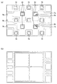
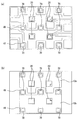
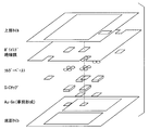
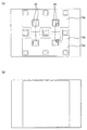
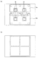
下側の高熱伝導率絶縁基板1、2の各々はまた、2つの主表面として内側表面3、4および外側表面5、6を有する。上側高熱伝導率絶縁基板1の内側主表面3には、ゲート、ソースまたはエミッタ、およびアノード用の外部バス電極パターン7a、7b、8a、8b、9a、9b、9c、が、図3(a)の高熱伝導率絶縁基板1の平面図に示す通り配設されている。下側高熱伝導率絶縁基板2の内側主表面4には、図4(a)に示すように、ドレインまたはコレクタ、およびカソード用の外部バス電極パターン10a、10bが配設されている。なお、図3(b)及び図4(b)は、上側および下側の高熱伝導率絶縁基板1、2の外側主表面5,6のレイアウトを示しており、これら外側主表面5,6には、後述する熱交換器80との結合のため、リッジ43が形成されている。
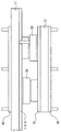
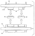
1 上側高熱伝導率絶縁非平面基板
2 下側高熱伝導率絶縁非平面基板
3、4 内側表面
5、6 外側表面
7〜10 金属電極
20 半導体トランジスタチップ(ダイ)
23 ソースまたはコレクタ電極
24 ゲート電極
25 ドレインまたはエミッタ電極
30 半導体ダイオードチップ(ダイ)
33 アノード電極
34 カソード電極
43 リッジ
45 はんだ
70 電気絶縁領域
77 非伝導性セラミック基板
80 熱交換器
Claims (29)
- 第1および第2の高熱伝導率絶縁非平面基板と、
前記第1および第2の高熱伝導率絶縁非平面基板の間に配置される、複数の半導体チップ及び電子部品とを備え、
前記第1および第2の高熱伝導率絶縁非平面基板の各々は、電気絶縁体層および複数のパターン形成された電気導体層を含み、それらは交互に積み重ねられており、
前記電気導体層は、機械的および電気的に前記半導体チップおよび前記電子部品と接続され、
前記第1および第2の高熱伝導率絶縁非平面基板の各々は、さらに、複数の隆起領域、すなわちポストを含み、当該隆起領域、すなわちポストは、前記第1および第2の高熱伝導率絶縁非平面基板が機械的および電気的に接続されるように、はんだ層を介して相互に結合され、
前記隆起領域、すなわちポストの数、配置、および各々の隆起領域、すなわちポストの形状は、前記第1および第2の高熱伝導率絶縁非平面基板の間に機械的分離をもたらすように調整され、
前記電気導体層は、複数の電気回路が前記第1および第2の高熱伝導率絶縁非平面基板のうちの少なくとも一方に設けられるように、互いに分離絶縁されることを特徴とするパワーエレクトロニックパッケージ。 - 前記第1および第2の高熱伝導率絶縁非平面基板の一方は、複数の凹部を含み、当該複数の凹部は、前記第1および第2の高熱伝導率絶縁非平面基板の一方の所定領域に配置され、その所定領域には、前記半導体チップまたは電子部品が搭載され、
前記第1および第2の高熱伝導率絶縁非平面基板は、複数の結合領域によって、機械的および電気的に結合され、前記隆起領域、すなわちポストが、その結合領域を提供することを特徴とする請求項1に記載のパワーエレクトロニックパッケージ。 - 前記第1の高熱伝導率絶縁非平面基板は、いずれの凹部も有していない平坦な表面を備えることを特徴とする請求項2に記載のパワーエレクトロニックパッケージ。
- 前記隆起領域、すなわちポストは、前記第1および第2の高熱伝導率絶縁非平面基板間において、複数の結合領域を提供し、それら複数の結合領域は、前記第1および第2の高熱伝導率絶縁非平面基板の少なくとも一方と、外部の電気回路とが結合可能な配列を有することを特徴とする請求項1に記載のパワーエレクトロニックパッケージ。
- 各々の半導体チップは、第1および第2の主電極を有し、
前記第1の主電極は、前記半導体チップの第1の主表面に配置され、
前記第2の主電極は、前記半導体チップの第2の主表面に配置され、
前記第2の主表面は、前記第1の主表面と対向していることを特徴とする請求項1に記載のパワーエレクトロニックパッケージ。 - 前記第1および第2の高熱伝導率絶縁非平面基板の各々は、第1及び第2の外部表面を有し、
前記第1の外部表面は、前記半導体チップの一つの電極と、前記電子部品の一つの電極との接続に供され、前記第1の外部表面が、両サイドにおける電気的接続のための複数の外部バスを提供することを特徴とする請求項5に記載のパワーエレクトロニックパッケージ。 - 前記半導体チップは、半導体トランジスタチップを含み、
前記電子部品は、ダイオードチップを含み、
前記外部バスは、前記半導体トランジスタチップの第1の主電極と、前記ダイオードチップの第1の主電極との間の接続のための第1の外部バスを含むことを特徴とする請求項6に記載のパワーエレクトロニックパッケージ。 - 前記外部バスは、前記トランジスタチップの第2の主電極と、前記ダイオードチップの第2の主電極との間の接続のための第2の外部バスをさらに含むことを特徴とする請求項7に記載のパワーエレクトロニックパッケージ。
- 前記半導体チップ及び前記電子部品は、前記第1および第2の高熱伝導率絶縁非平面基板の第1の外部表面の間に挟まれることを特徴とする請求項6に記載のパワーエレクトロニックパッケージ。
- 前記結合領域は、複数の電気的に不活性なボンド領域を含み、前記電気的に不活性なボンド領域の数、前記電気的に不活性なボンド領域の配列、及び電気的に不活性なボンド領域の各々の形状が、前記第1および第2の高熱伝導率絶縁非平面基板の機械的分離をもたらすように調整されることを特徴とする請求項2に記載のパワーエレクトロニックパッケージ。
- 前記第1および第2の高熱伝導率絶縁非平面基板の各々は、非結合領域を含み、この非結合領域は、前記結合領域の高さよりも低い高さを有することを特徴とする請求項2に記載のパワーエレクトロニックパッケージ。
- 前記半導体チップの一つの電極、前記電子部品の一つの電極、及び前記外部バスは、はんだ付け可能な電気導通材料を用いて接合されることを特徴とする請求項6に記載のパワーエレクトロニックパッケージ。
- 前記第1および第2の高熱伝導率絶縁非平面基板は、挟持部分の絶縁樹脂を介して接続されており、当該絶縁樹脂は、エポキシ樹脂またはシリコーン樹脂であって、前記半導体チップを覆うとともに、前記第1および第2の高熱伝導率絶縁非平面基板の前記外部バス間を電気的に絶縁するものであることを特徴とする請求項6に記載のパワーエレクトロニックパッケージ。
- 前記第1および第2の高熱伝導率絶縁非平面基板は、挟持部分の絶縁ポリアミド層を介して接続されており、当該絶縁ポリアミド層は、前記半導体チップと前記電子部品を覆うとともに、前記第1および第2の高熱伝導率絶縁非平面基板の前記外部バス間を電気的に絶縁するものであることを特徴とする請求項6に記載のパワーエレクトロニックパッケージ。
- 前記第1および第2の高熱伝導率絶縁非平面基板の各々は、非導電性セラミック基板と、高導電性金属部材とを有し、前記第1および第2の高熱伝導率絶縁非平面基板の高導電性金属部材は、ダイレクトボンディング銅、ダイレクトボンディングアルミニウムまたは活性金属ブレージングはんだ材料によって前記基板に結合されたものであることを特徴とする請求項1に記載のパワーエレクトロニックパッケージ。
- 非導電性セラミック基板は、2種の材料からなり、1つは、アルミナ、窒化アルミニウム、窒化ケイ素、炭化ケイ素及びダイヤモンドのいずれかであり、他の1つは、銅またはアルミニウムであることを特徴とする請求項15に記載のパワーエレクトロニックパッケージ。
- 前記第1および第2の高熱伝導率絶縁非平面基板の各々は、銅またはアルミニウムを含むことを特徴とする請求項1に記載のパワーエレクトロニックパッケージ。
- 前記外部バスは、前記第1および第2の高熱伝導率絶縁非平面基板の各々に配設されるものであり、銅もしくはアルミニウムを使用した、1ボンド・2ステップエッチング法によって形成されえるものであることを特徴とする請求項6に記載のパワーエレクトロニックパッケージ。
- 前記外部バスは、前記第1および第2の高熱伝導率絶縁非平面基板の各々に配設されるものであり、銅もしくはアルミニウムを使用した、2ボンド・2ステップエッチング法によって形成されえるものであることを特徴とする請求項6に記載のパワーエレクトロニックパッケージ。
- 前記半導体チップは、縦型の接合形電界効果トランジスタ(JFET)を含むことを特徴とする請求項1に記載のパワーエレクトロニックパッケージ。
- 前記半導体チップは、縦型のMOS形電界効果トランジスタ(MOSFET)を含むことを特徴とする請求項1に記載のパワーエレクトロニックパッケージ。
- 前記半導体チップは、縦型の絶縁ゲート形バイポーラトランジスタ(IGBT)を含むことを特徴とする請求項1に記載のパワーエレクトロニックパッケージ。
- 前記半導体チップは、縦型の接合ダイオードを含むことを特徴とする請求項1に記載のパワーエレクトロニックパッケージ。
- 前記半導体チップは、縦型のショットキーバリヤダイオードを含むことを特徴とする請求項1に記載のパワーエレクトロニックパッケージ。
- 前記半導体チップは、縦型のワイドバンドギャップ半導体トランジスタを含み、前記電子部品はダイオードチップを含むことを特徴とする請求項1に記載のパワーエレクトロニックパッケージ。
- 前記半導体チップは、縦型のSiCトランジスタを含み、前記電子部品はダイオードチップを含むことを特徴とする請求項1に記載のパワーエレクトロニックパッケージ。
- 最大動作温度よりも高いプロセス温度の下で形成されることにより、残留圧縮応力が前記電子部品において減少されることを特徴とする請求項1に記載のパワーエレクトロニックパッケージ。
- 前記第1の高熱伝導率絶縁非平面基板に装着された第1の熱交換器と、
前記第2の高熱伝導率絶縁非平面基板に装着された第2の熱交換器とをさらに備え、
前記第1及び第2の熱交換器は、互いに並列に配置され、
前記熱交換器の各々は、第1および第2表面を有し、前記第1の熱交換器の第1表面は、前記第1の高熱伝導率絶縁非平面基板に接触し、前記第2の熱交換器の第1表面は、前記第2の高熱伝導率絶縁非平面基板に接触することを特徴とする請求項1に記載のパワーエレクトロニックパッケージ。 - 前記第1の熱交換器の第2表面に取り付けられるDCリンクキャパシタボードと、
前記第2の熱交換器の第2表面に取り付けられるゲートドライバユニットとを備え、
前記DCリンクキャパシタボードと前記ゲートドライバユニットとが、冷却インバーターシステムを提供し、各々の熱交換器のすべての表面が冷却のために利用されることを特徴とする請求項28に記載のパワーエレクトロニックパッケージ。
Applications Claiming Priority (2)
| Application Number | Priority Date | Filing Date | Title |
|---|---|---|---|
| US11/511,516 US7999369B2 (en) | 2006-08-29 | 2006-08-29 | Power electronic package having two substrates with multiple semiconductor chips and electronic components |
| US11/511516 | 2006-08-29 |
Publications (2)
| Publication Number | Publication Date |
|---|---|
| JP2008060531A JP2008060531A (ja) | 2008-03-13 |
| JP5374831B2 true JP5374831B2 (ja) | 2013-12-25 |
Family
ID=39150347
Family Applications (1)
| Application Number | Title | Priority Date | Filing Date |
|---|---|---|---|
| JP2007126042A Expired - Fee Related JP5374831B2 (ja) | 2006-08-29 | 2007-05-10 | 複数の半導体チップおよび電子部品を備える2枚の基板を有するパワーエレクトロニックパッケージ |
Country Status (2)
| Country | Link |
|---|---|
| US (2) | US7999369B2 (ja) |
| JP (1) | JP5374831B2 (ja) |
Cited By (4)
| Publication number | Priority date | Publication date | Assignee | Title |
|---|---|---|---|---|
| US10032689B2 (en) | 2016-10-06 | 2018-07-24 | Hyundai Motor Company | Double-side cooling type power module and producing method thereof |
| KR101899788B1 (ko) * | 2017-02-22 | 2018-11-05 | 제엠제코(주) | 양면 방열구조를 갖는 반도체 패키지 및 그 제조 방법 |
| TWI856412B (zh) * | 2021-11-08 | 2024-09-21 | 銓心半導體異質整合股份有限公司 | 金剛石增強的先進ic與先進ic封裝 |
| US12593688B2 (en) | 2022-08-08 | 2026-03-31 | nD-HI Technologies Lab, Inc. | Manufacturing method of diamond composite wafer |
Families Citing this family (118)
| Publication number | Priority date | Publication date | Assignee | Title |
|---|---|---|---|---|
| DE102007002807B4 (de) * | 2007-01-18 | 2014-08-14 | Infineon Technologies Ag | Chipanordnung |
| US8421214B2 (en) * | 2007-10-10 | 2013-04-16 | Vishay General Semiconductor Llc | Semiconductor device and method for manufacturing a semiconductor device |
| US8955215B2 (en) | 2009-05-28 | 2015-02-17 | Hsio Technologies, Llc | High performance surface mount electrical interconnect |
| US9536815B2 (en) | 2009-05-28 | 2017-01-03 | Hsio Technologies, Llc | Semiconductor socket with direct selective metalization |
| US9276336B2 (en) | 2009-05-28 | 2016-03-01 | Hsio Technologies, Llc | Metalized pad to electrical contact interface |
| WO2011153298A1 (en) | 2010-06-03 | 2011-12-08 | Hsio Technologies, Llc | Electrical connector insulator housing |
| US9232654B2 (en) | 2009-06-02 | 2016-01-05 | Hsio Technologies, Llc | High performance electrical circuit structure |
| WO2010141316A1 (en) | 2009-06-02 | 2010-12-09 | Hsio Technologies, Llc | Compliant printed circuit wafer probe diagnostic tool |
| US9930775B2 (en) | 2009-06-02 | 2018-03-27 | Hsio Technologies, Llc | Copper pillar full metal via electrical circuit structure |
| US9318862B2 (en) | 2009-06-02 | 2016-04-19 | Hsio Technologies, Llc | Method of making an electronic interconnect |
| WO2010141313A1 (en) | 2009-06-02 | 2010-12-09 | Hsio Technologies, Llc | Compliant printed circuit socket diagnostic tool |
| WO2010141297A1 (en) | 2009-06-02 | 2010-12-09 | Hsio Technologies, Llc | Compliant printed circuit wafer level semiconductor package |
| US8988093B2 (en) | 2009-06-02 | 2015-03-24 | Hsio Technologies, Llc | Bumped semiconductor wafer or die level electrical interconnect |
| US9277654B2 (en) | 2009-06-02 | 2016-03-01 | Hsio Technologies, Llc | Composite polymer-metal electrical contacts |
| US9613841B2 (en) | 2009-06-02 | 2017-04-04 | Hsio Technologies, Llc | Area array semiconductor device package interconnect structure with optional package-to-package or flexible circuit to package connection |
| US9276339B2 (en) | 2009-06-02 | 2016-03-01 | Hsio Technologies, Llc | Electrical interconnect IC device socket |
| WO2010141295A1 (en) | 2009-06-02 | 2010-12-09 | Hsio Technologies, Llc | Compliant printed flexible circuit |
| WO2010141311A1 (en) | 2009-06-02 | 2010-12-09 | Hsio Technologies, Llc | Compliant printed circuit area array semiconductor device package |
| US9320133B2 (en) | 2009-06-02 | 2016-04-19 | Hsio Technologies, Llc | Electrical interconnect IC device socket |
| WO2012074963A1 (en) | 2010-12-01 | 2012-06-07 | Hsio Technologies, Llc | High performance surface mount electrical interconnect |
| US9603249B2 (en) | 2009-06-02 | 2017-03-21 | Hsio Technologies, Llc | Direct metalization of electrical circuit structures |
| WO2010141266A1 (en) | 2009-06-02 | 2010-12-09 | Hsio Technologies, Llc | Compliant printed circuit peripheral lead semiconductor package |
| US9196980B2 (en) | 2009-06-02 | 2015-11-24 | Hsio Technologies, Llc | High performance surface mount electrical interconnect with external biased normal force loading |
| US9699906B2 (en) | 2009-06-02 | 2017-07-04 | Hsio Technologies, Llc | Hybrid printed circuit assembly with low density main core and embedded high density circuit regions |
| US9184145B2 (en) | 2009-06-02 | 2015-11-10 | Hsio Technologies, Llc | Semiconductor device package adapter |
| US8970031B2 (en) * | 2009-06-16 | 2015-03-03 | Hsio Technologies, Llc | Semiconductor die terminal |
| US8618649B2 (en) | 2009-06-02 | 2013-12-31 | Hsio Technologies, Llc | Compliant printed circuit semiconductor package |
| WO2010141303A1 (en) | 2009-06-02 | 2010-12-09 | Hsio Technologies, Llc | Resilient conductive electrical interconnect |
| WO2010147782A1 (en) | 2009-06-16 | 2010-12-23 | Hsio Technologies, Llc | Simulated wirebond semiconductor package |
| US9320144B2 (en) | 2009-06-17 | 2016-04-19 | Hsio Technologies, Llc | Method of forming a semiconductor socket |
| US8984748B2 (en) | 2009-06-29 | 2015-03-24 | Hsio Technologies, Llc | Singulated semiconductor device separable electrical interconnect |
| US8981809B2 (en) | 2009-06-29 | 2015-03-17 | Hsio Technologies, Llc | Compliant printed circuit semiconductor tester interface |
| JP5500936B2 (ja) * | 2009-10-06 | 2014-05-21 | イビデン株式会社 | 回路基板及び半導体モジュール |
| US8410601B2 (en) * | 2009-11-15 | 2013-04-02 | Microsemi Corporation | RF package |
| US8034666B2 (en) * | 2009-11-15 | 2011-10-11 | Microsemi Corporation | Multi-layer thick-film RF package |
| US8064202B2 (en) * | 2010-02-24 | 2011-11-22 | Monolithic Power Systems, Inc. | Sandwich structure with double-sided cooling and EMI shielding |
| JP5921055B2 (ja) * | 2010-03-08 | 2016-05-24 | ルネサスエレクトロニクス株式会社 | 半導体装置 |
| US8525334B2 (en) * | 2010-04-27 | 2013-09-03 | International Rectifier Corporation | Semiconductor on semiconductor substrate multi-chip-scale package |
| US10159154B2 (en) | 2010-06-03 | 2018-12-18 | Hsio Technologies, Llc | Fusion bonded liquid crystal polymer circuit structure |
| US9689897B2 (en) | 2010-06-03 | 2017-06-27 | Hsio Technologies, Llc | Performance enhanced semiconductor socket |
| US9350093B2 (en) | 2010-06-03 | 2016-05-24 | Hsio Technologies, Llc | Selective metalization of electrical connector or socket housing |
| US9412727B2 (en) | 2011-09-20 | 2016-08-09 | Semprius, Inc. | Printing transferable components using microstructured elastomeric surfaces with pressure modulated reversible adhesion |
| US9673163B2 (en) * | 2011-10-18 | 2017-06-06 | Rohm Co., Ltd. | Semiconductor device with flip chip structure and fabrication method of the semiconductor device |
| JP2013098451A (ja) * | 2011-11-04 | 2013-05-20 | Sumitomo Electric Ind Ltd | 半導体装置及び配線基板 |
| JP5979478B2 (ja) * | 2012-01-16 | 2016-08-24 | 国立研究開発法人産業技術総合研究所 | 3層構造積層ダイヤモンド系基板、パワー半導体モジュール用放熱実装基板およびそれらの製造方法 |
| JP5661052B2 (ja) * | 2012-01-18 | 2015-01-28 | 三菱電機株式会社 | パワー半導体モジュールおよびその製造方法 |
| JP6083109B2 (ja) * | 2012-01-18 | 2017-02-22 | 富士電機株式会社 | 半導体装置 |
| US9761506B2 (en) * | 2012-02-23 | 2017-09-12 | Rohm Co., Ltd. | Semiconductor device and fabrication method for the same |
| JP6104518B2 (ja) | 2012-04-27 | 2017-03-29 | 日産自動車株式会社 | 半導体装置の製造方法、断熱荷重治具及び断熱荷重治具の設置方法 |
| CN102664177B (zh) * | 2012-05-16 | 2014-10-29 | 中国科学院电工研究所 | 一种双面冷却的功率半导体模块 |
| US9761520B2 (en) | 2012-07-10 | 2017-09-12 | Hsio Technologies, Llc | Method of making an electrical connector having electrodeposited terminals |
| US8941208B2 (en) | 2012-07-30 | 2015-01-27 | General Electric Company | Reliable surface mount integrated power module |
| JP2014032985A (ja) * | 2012-08-01 | 2014-02-20 | Rohm Co Ltd | 半導体装置およびその製造方法 |
| KR101482317B1 (ko) * | 2012-10-30 | 2015-01-13 | 삼성전기주식회사 | 단위 전력 모듈 및 이를 포함하는 전력 모듈 패키지 |
| US9312193B2 (en) | 2012-11-09 | 2016-04-12 | Taiwan Semiconductor Manufacturing Company, Ltd. | Stress relief structures in package assemblies |
| JP5966921B2 (ja) * | 2012-12-28 | 2016-08-10 | トヨタ自動車株式会社 | 半導体モジュールの製造方法 |
| KR102034717B1 (ko) * | 2013-02-07 | 2019-10-21 | 삼성전자주식회사 | 파워모듈용 기판, 파워모듈용 터미널 및 이들을 포함하는 파워모듈 |
| US10269688B2 (en) | 2013-03-14 | 2019-04-23 | General Electric Company | Power overlay structure and method of making same |
| US8987876B2 (en) | 2013-03-14 | 2015-03-24 | General Electric Company | Power overlay structure and method of making same |
| KR20140141281A (ko) * | 2013-05-31 | 2014-12-10 | 삼성전자주식회사 | 반도체 패키지 |
| US10667410B2 (en) | 2013-07-11 | 2020-05-26 | Hsio Technologies, Llc | Method of making a fusion bonded circuit structure |
| US10506722B2 (en) | 2013-07-11 | 2019-12-10 | Hsio Technologies, Llc | Fusion bonded liquid crystal polymer electrical circuit structure |
| JP6315650B2 (ja) * | 2013-07-31 | 2018-04-25 | 太陽誘電株式会社 | 電子デバイス |
| EP2889903A1 (en) * | 2013-12-24 | 2015-07-01 | Nxp B.V. | Die with a multilayer backside interface layer for solder bonding to a substrate and corresponding manufacturing method |
| US20170207193A1 (en) * | 2014-07-20 | 2017-07-20 | X-Celeprint Limited | Apparatus and methods for micro-transfer-printing |
| FR3025691B1 (fr) * | 2014-09-08 | 2016-10-07 | Schneider Electric Ind Sas | Module electronique haute puissance et procede de fabrication d'un tel module |
| TWI539894B (zh) | 2014-11-28 | 2016-06-21 | 財團法人工業技術研究院 | 功率模組 |
| US10680518B2 (en) * | 2015-03-16 | 2020-06-09 | Cree, Inc. | High speed, efficient SiC power module |
| US9755335B2 (en) | 2015-03-18 | 2017-09-05 | Hsio Technologies, Llc | Low profile electrical interconnect with fusion bonded contact retention and solder wick reduction |
| WO2016174899A1 (ja) | 2015-04-27 | 2016-11-03 | 富士電機株式会社 | 半導体装置 |
| US9704821B2 (en) | 2015-08-11 | 2017-07-11 | X-Celeprint Limited | Stamp with structured posts |
| ITUB20153344A1 (it) * | 2015-09-02 | 2017-03-02 | St Microelectronics Srl | Modulo di potenza elettronico con migliorata dissipazione termica e relativo metodo di fabbricazione |
| WO2017054855A1 (en) * | 2015-09-30 | 2017-04-06 | Agile Power Switch 3D - Integration Apsi3D | A semiconductor power device comprising additional tracks and method of manufacturing the semiconductor power device |
| US9698076B1 (en) | 2015-12-22 | 2017-07-04 | Ksr Ip Holdings Llc. | Metal slugs for double-sided cooling of power module |
| US10403601B2 (en) * | 2016-06-17 | 2019-09-03 | Fairchild Semiconductor Corporation | Semiconductor package and related methods |
| DE102016121801B4 (de) | 2016-11-14 | 2022-03-17 | Infineon Technologies Ag | Baugruppe mit Verbindungen, die verschiedene Schmelztemperaturen aufweisen, Fahrzeug mit der Baugruppe und Verfahren zum Herstellen derselben und Verwendung der Baugruppe für eine Automobilanwendung |
| KR101956996B1 (ko) * | 2016-12-15 | 2019-06-24 | 현대자동차주식회사 | 양면냉각형 파워모듈 |
| FR3062518B1 (fr) | 2017-01-31 | 2019-04-19 | Supergrid Institute | Module electronique de puissance comportant un support dielectrique |
| JP6809294B2 (ja) * | 2017-03-02 | 2021-01-06 | 三菱電機株式会社 | パワーモジュール |
| DE102017208925A1 (de) | 2017-05-29 | 2018-11-29 | Zf Friedrichshafen Ag | Power Electronic Packaging |
| CN111357099B (zh) | 2017-09-15 | 2024-05-03 | 费纳模组有限公司 | 电子器件的封装方法和接合技术 |
| JP2019057576A (ja) * | 2017-09-20 | 2019-04-11 | ルネサスエレクトロニクス株式会社 | 半導体装置 |
| JP7004749B2 (ja) * | 2018-01-25 | 2022-01-21 | 三菱電機株式会社 | 回路装置および電力変換装置 |
| JP6999462B2 (ja) * | 2018-03-26 | 2022-01-18 | 日立Astemo株式会社 | パワー半導体装置 |
| EP3547367A1 (en) * | 2018-03-30 | 2019-10-02 | Mitsubishi Electric R&D Centre Europe B.V. | Power module incorporating pre-packed power cells |
| IT201800004209A1 (it) | 2018-04-05 | 2019-10-05 | Dispositivo semiconduttore di potenza con relativo incapsulamento e corrispondente procedimento di fabbricazione | |
| TWI716680B (zh) * | 2018-04-16 | 2021-01-21 | 吳文湖 | 多段式雙串聯多晶組結構二極體元件 |
| EP3557614A1 (de) * | 2018-04-17 | 2019-10-23 | Siemens Aktiengesellschaft | Leistungsmodul mit einem leistungselektronischen bauelement auf einer substratplatte und leistungselektronische schaltung mit einem solchen leistungsmodul |
| US11075137B2 (en) * | 2018-05-02 | 2021-07-27 | Semiconductor Components Industries, Llc | High power module package structures |
| DE102019003027A1 (de) | 2018-05-02 | 2019-11-07 | Semiconductor Components Lndustries Llc | Paketstrukturen für hochleistungsmodule |
| EP3584833B1 (en) | 2018-06-19 | 2021-09-01 | Mitsubishi Electric R&D Centre Europe B.V. | Power module with improved alignment |
| SG11202100905XA (en) * | 2018-08-08 | 2021-02-25 | Agency Science Tech & Res | Semiconductor package and method of forming the same |
| KR102574378B1 (ko) | 2018-10-04 | 2023-09-04 | 현대자동차주식회사 | 파워모듈 |
| KR102645198B1 (ko) * | 2018-10-24 | 2024-03-06 | 현대자동차주식회사 | 양면 냉각형 파워모듈 |
| US10748793B1 (en) | 2019-02-13 | 2020-08-18 | X Display Company Technology Limited | Printing component arrays with different orientations |
| FR3095778B1 (fr) | 2019-05-06 | 2022-06-03 | Safran | Procede de fabrication d’un module electronique de puissance |
| US11621211B2 (en) * | 2019-06-14 | 2023-04-04 | Mediatek Inc. | Semiconductor package structure |
| IT201900013743A1 (it) | 2019-08-01 | 2021-02-01 | St Microelectronics Srl | Dispositivo elettronico di potenza incapsulato, in particolare circuito a ponte comprendente transistori di potenza, e relativo procedimento di assemblaggio |
| JP7268563B2 (ja) * | 2019-09-30 | 2023-05-08 | 株式会社デンソー | 半導体装置 |
| US11062936B1 (en) | 2019-12-19 | 2021-07-13 | X Display Company Technology Limited | Transfer stamps with multiple separate pedestals |
| CN115023791B (zh) | 2020-01-28 | 2025-08-26 | 力特保险丝公司 | 半导体芯片封装件和组装方法 |
| JP7306294B2 (ja) | 2020-02-19 | 2023-07-11 | 株式会社デンソー | 半導体モジュール |
| US11967899B2 (en) | 2020-05-22 | 2024-04-23 | Marel Power Solutions | Fluid cooled inverter |
| IT202000016840A1 (it) | 2020-07-10 | 2022-01-10 | St Microelectronics Srl | Dispositivo mosfet incapsulato ad alta tensione e dotato di clip di connessione e relativo procedimento di fabbricazione |
| EP3975225A1 (en) | 2020-09-24 | 2022-03-30 | Infineon Technologies Austria AG | Semiconductor module |
| EP3989274A1 (en) * | 2020-10-23 | 2022-04-27 | SwissSEM Technologies AG | Power module |
| KR102588851B1 (ko) * | 2021-04-14 | 2023-10-16 | 주식회사 아모센스 | 파워모듈 및 그 제조방법 |
| CN113658871B (zh) * | 2021-06-27 | 2024-08-02 | 厦门芯光润泽科技有限公司 | 一种功率模块的制造方法 |
| CN116072630A (zh) | 2021-10-29 | 2023-05-05 | 意法半导体股份有限公司 | 半导体封装、封装形成方法和电子设备 |
| WO2023132595A1 (ko) * | 2022-01-04 | 2023-07-13 | 주식회사 아모센스 | 세라믹 기판 유닛 및 그 제조방법 |
| CN114664758A (zh) * | 2022-03-20 | 2022-06-24 | 上海沛塬电子有限公司 | 一种高频大功率封装模组及其制作方法 |
| US12191264B2 (en) * | 2022-04-06 | 2025-01-07 | Semiconductor Components Industries, Llc | Thermal performance improvement and stress reduction in semiconductor device modules |
| CN117316908A (zh) * | 2022-06-22 | 2023-12-29 | 无锡华润安盛科技有限公司 | 封装结构及其制作方法 |
| US12122251B2 (en) * | 2022-09-28 | 2024-10-22 | BorgWarner US Technologies LLC | Systems and methods for bidirectional message architecture for inverter for electric vehicle |
| US12568609B2 (en) * | 2023-07-11 | 2026-03-03 | Hamilton Sundstrand Corporation | Thermal management systems for rectifier assemblies |
| JP2025151720A (ja) * | 2024-03-28 | 2025-10-09 | 株式会社タムラ製作所 | パワー半導体モジュール |
| EP4709133A1 (en) * | 2024-08-30 | 2026-03-11 | Shenzhen STS Microelectronics Co., Ltd. | Dual-side cooling power modules and manufacturing methods thereof, and electrical systems |
| CN119050076B (zh) * | 2024-10-29 | 2025-03-25 | 北京怀柔实验室 | 半导体封装结构 |
Family Cites Families (30)
| Publication number | Priority date | Publication date | Assignee | Title |
|---|---|---|---|---|
| DE4317215A1 (de) | 1993-05-24 | 1994-12-01 | Abb Research Ltd | Hochspannungsbauelement |
| JP3879150B2 (ja) * | 1996-08-12 | 2007-02-07 | 株式会社デンソー | 半導体装置 |
| DE59713027D1 (de) * | 1996-09-30 | 2010-03-25 | Infineon Technologies Ag | Mikroelektronisches bauteil in sandwich-bauweise |
| WO2000019515A1 (en) * | 1998-09-30 | 2000-04-06 | Seiko Epson Corporation | Semiconductor device and manufacturing method thereof, circuit board and electronic equipment |
| US6072240A (en) * | 1998-10-16 | 2000-06-06 | Denso Corporation | Semiconductor chip package |
| FR2786657B1 (fr) | 1998-11-27 | 2001-06-01 | Alstom Technology | Composant electronique de puissance comportant des moyens de refroidissement et procede de fabrication d'un tel composant |
| JP2000174180A (ja) * | 1998-12-02 | 2000-06-23 | Shibafu Engineering Kk | 半導体装置 |
| DE19914815A1 (de) * | 1999-03-31 | 2000-10-05 | Abb Research Ltd | Halbleitermodul |
| US7138708B2 (en) * | 1999-09-24 | 2006-11-21 | Robert Bosch Gmbh | Electronic system for fixing power and signal semiconductor chips |
| EP2234154B1 (en) * | 2000-04-19 | 2016-03-30 | Denso Corporation | Coolant cooled type semiconductor device |
| JP3923258B2 (ja) * | 2001-01-17 | 2007-05-30 | 松下電器産業株式会社 | 電力制御系電子回路装置及びその製造方法 |
| JP4811756B2 (ja) | 2001-09-28 | 2011-11-09 | Dowaメタルテック株式会社 | 金属−セラミックス接合回路基板の製造方法 |
| JP4168114B2 (ja) | 2001-09-28 | 2008-10-22 | Dowaホールディングス株式会社 | 金属−セラミックス接合体 |
| US6812553B2 (en) * | 2002-01-16 | 2004-11-02 | Delphi Technologies, Inc. | Electrically isolated and thermally conductive double-sided pre-packaged component |
| US20040094828A1 (en) | 2002-01-16 | 2004-05-20 | Delphi Technologies, Inc. | Double-sided multi-chip circuit component |
| JP3841007B2 (ja) * | 2002-03-28 | 2006-11-01 | 株式会社デンソー | 半導体装置 |
| DE10221082A1 (de) * | 2002-05-11 | 2003-11-20 | Bosch Gmbh Robert | Halbleiterbauelement |
| DE10231091A1 (de) * | 2002-07-10 | 2004-01-22 | Robert Bosch Gmbh | Aktivgleichrichter-Modul für Drehstromgeneratoren von Fahrzeugen |
| US6946740B2 (en) * | 2002-07-15 | 2005-09-20 | International Rectifier Corporation | High power MCM package |
| US7045884B2 (en) | 2002-10-04 | 2006-05-16 | International Rectifier Corporation | Semiconductor device package |
| US7009291B2 (en) * | 2002-12-25 | 2006-03-07 | Denso Corporation | Semiconductor module and semiconductor device |
| US7129577B2 (en) * | 2003-02-27 | 2006-10-31 | Power-One, Inc. | Power supply packaging system |
| JP4022758B2 (ja) * | 2003-03-31 | 2007-12-19 | 株式会社デンソー | 半導体装置 |
| JP4362597B2 (ja) * | 2003-05-30 | 2009-11-11 | Dowaメタルテック株式会社 | 金属−セラミックス回路基板およびその製造方法 |
| JP4594237B2 (ja) | 2003-09-04 | 2010-12-08 | パナソニック株式会社 | 半導体装置 |
| JP4491244B2 (ja) * | 2004-01-07 | 2010-06-30 | 三菱電機株式会社 | 電力半導体装置 |
| DE102004050792A1 (de) | 2004-10-19 | 2006-04-20 | Robert Bosch Gmbh | Bauelemente-Modul für Hochtemperaturanwendungen und Verfahren zum Herstellen eines derartigen Bauelemente-Moduls |
| US7521789B1 (en) * | 2004-12-18 | 2009-04-21 | Rinehart Motion Systems, Llc | Electrical assembly having heat sink protrusions |
| US7331796B2 (en) * | 2005-09-08 | 2008-02-19 | International Business Machines Corporation | Land grid array (LGA) interposer utilizing metal-on-elastomer hemi-torus and other multiple points of contact geometries |
| US7557434B2 (en) * | 2006-08-29 | 2009-07-07 | Denso Corporation | Power electronic package having two substrates with multiple electronic components |
-
2006
- 2006-08-29 US US11/511,516 patent/US7999369B2/en not_active Expired - Fee Related
-
2007
- 2007-05-10 JP JP2007126042A patent/JP5374831B2/ja not_active Expired - Fee Related
-
2011
- 2011-06-29 US US13/171,788 patent/US8432030B2/en not_active Expired - Fee Related
Cited By (4)
| Publication number | Priority date | Publication date | Assignee | Title |
|---|---|---|---|---|
| US10032689B2 (en) | 2016-10-06 | 2018-07-24 | Hyundai Motor Company | Double-side cooling type power module and producing method thereof |
| KR101899788B1 (ko) * | 2017-02-22 | 2018-11-05 | 제엠제코(주) | 양면 방열구조를 갖는 반도체 패키지 및 그 제조 방법 |
| TWI856412B (zh) * | 2021-11-08 | 2024-09-21 | 銓心半導體異質整合股份有限公司 | 金剛石增強的先進ic與先進ic封裝 |
| US12593688B2 (en) | 2022-08-08 | 2026-03-31 | nD-HI Technologies Lab, Inc. | Manufacturing method of diamond composite wafer |
Also Published As
| Publication number | Publication date |
|---|---|
| JP2008060531A (ja) | 2008-03-13 |
| US8432030B2 (en) | 2013-04-30 |
| US7999369B2 (en) | 2011-08-16 |
| US20110254177A1 (en) | 2011-10-20 |
| US20080054439A1 (en) | 2008-03-06 |
Similar Documents
| Publication | Publication Date | Title |
|---|---|---|
| JP5374831B2 (ja) | 複数の半導体チップおよび電子部品を備える2枚の基板を有するパワーエレクトロニックパッケージ | |
| US7557434B2 (en) | Power electronic package having two substrates with multiple electronic components | |
| KR100430772B1 (ko) | 반도체장치 | |
| US9691673B2 (en) | Power module semiconductor device | |
| CN100373604C (zh) | 高功率mcm封装 | |
| CN107039297A (zh) | 电极端子、半导体装置以及电力变换装置 | |
| KR20200044635A (ko) | 반도체 서브 어셈블리 및 반도체 파워 모듈 | |
| CN101136396B (zh) | 包括两片带有多个半导体芯片和电子元件的衬底的功率电子封装件 | |
| CN111354710B (zh) | 半导体装置及其制造方法 | |
| US20250253198A1 (en) | Semiconductor package, electronic device, and method for manufacturing semiconductor package | |
| US20240047433A1 (en) | Semiconductor device | |
| CN115206919A (zh) | 半导体装置 | |
| US20050208750A1 (en) | Method of making cascaded die mountings with springs-loaded contact-bond options | |
| CN116895649A (zh) | 包括多个功率晶体管的封装电子器件 | |
| GB2485087A (en) | Power electronic package | |
| CN101136395A (zh) | 包括两片带有多个电子元件的衬底的功率电子封装件 | |
| JP6697547B2 (ja) | 追加的トラックを備えた半導体パワーデバイスおよび半導体パワーデバイスを製造する方法 | |
| JP2012238737A (ja) | 半導体モジュール及びその製造方法 | |
| GB2444978A (en) | Interconnections between two substrates in power electronic package for chips and components. | |
| US11450623B2 (en) | Semiconductor device | |
| CN111584422B (zh) | 半导体装置及其制造方法 | |
| US11837571B2 (en) | Semiconductor module comprising a first and second connecting element for connecting a semiconductor chip, and also production method | |
| JP4992302B2 (ja) | パワー半導体モジュール | |
| GB2444293A (en) | Double substrate power electronics package | |
| CN220324457U (zh) | 一种采用柔性连接片的低电感碳化硅模块 |
Legal Events
| Date | Code | Title | Description |
|---|---|---|---|
| A621 | Written request for application examination |
Free format text: JAPANESE INTERMEDIATE CODE: A621 Effective date: 20100507 |
|
| A977 | Report on retrieval |
Free format text: JAPANESE INTERMEDIATE CODE: A971007 Effective date: 20110629 |
|
| A131 | Notification of reasons for refusal |
Free format text: JAPANESE INTERMEDIATE CODE: A131 Effective date: 20120821 |
|
| A521 | Request for written amendment filed |
Free format text: JAPANESE INTERMEDIATE CODE: A523 Effective date: 20121116 |
|
| TRDD | Decision of grant or rejection written | ||
| A01 | Written decision to grant a patent or to grant a registration (utility model) |
Free format text: JAPANESE INTERMEDIATE CODE: A01 Effective date: 20130827 |
|
| A61 | First payment of annual fees (during grant procedure) |
Free format text: JAPANESE INTERMEDIATE CODE: A61 Effective date: 20130909 |
|
| R150 | Certificate of patent or registration of utility model |
Ref document number: 5374831 Country of ref document: JP Free format text: JAPANESE INTERMEDIATE CODE: R150 Free format text: JAPANESE INTERMEDIATE CODE: R150 |
|
| R250 | Receipt of annual fees |
Free format text: JAPANESE INTERMEDIATE CODE: R250 |
|
| R250 | Receipt of annual fees |
Free format text: JAPANESE INTERMEDIATE CODE: R250 |
|
| R250 | Receipt of annual fees |
Free format text: JAPANESE INTERMEDIATE CODE: R250 |
|
| R250 | Receipt of annual fees |
Free format text: JAPANESE INTERMEDIATE CODE: R250 |
|
| R250 | Receipt of annual fees |
Free format text: JAPANESE INTERMEDIATE CODE: R250 |
|
| R250 | Receipt of annual fees |
Free format text: JAPANESE INTERMEDIATE CODE: R250 |
|
| LAPS | Cancellation because of no payment of annual fees |